Vintage TI DataMath / Sinclair Scientific Calculator Emulator
by simpleavr in Circuits > Art
10157 Views, 87 Favorites, 0 Comments
Vintage TI DataMath / Sinclair Scientific Calculator Emulator
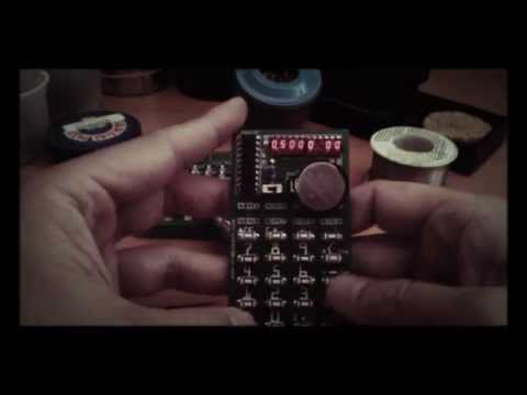
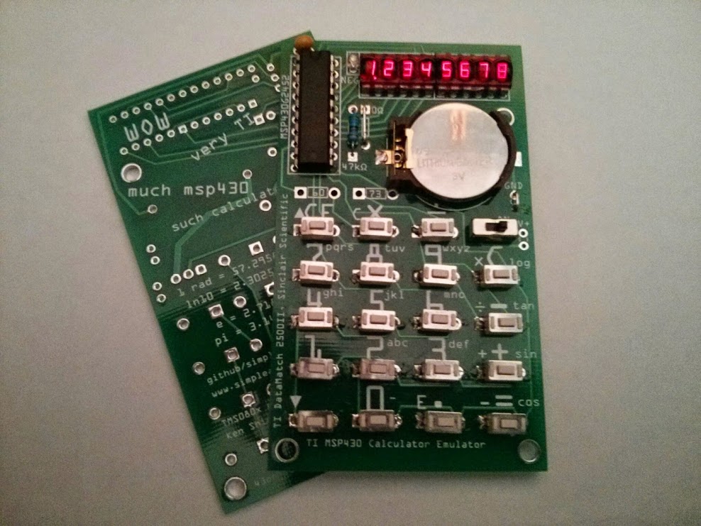
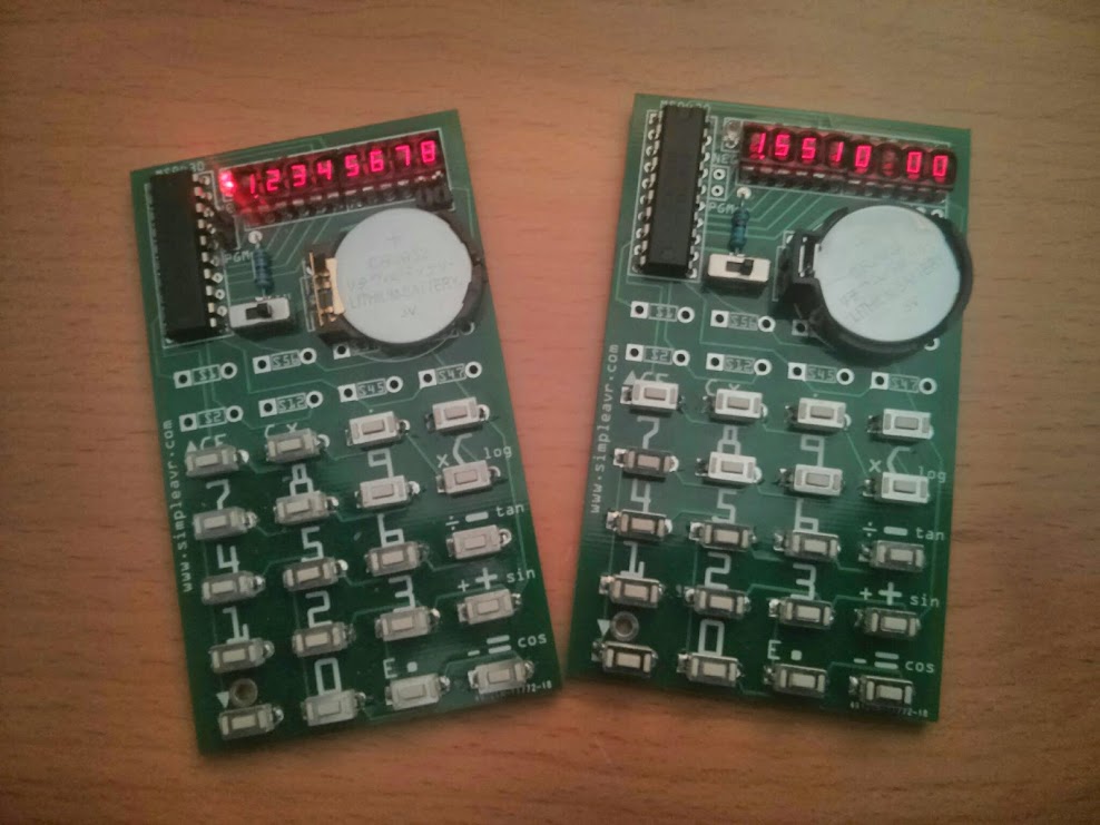
MSP430G2452 acting as a TMS0803 calculator chip. Emulates TI DataMath 2500II and Sinclair Scientific Calculators.
I got introduced to a web based calculator emulation via some forum thread.
I got interested and start playing w/ the idea of implementing the emulation on an msp430, my code is based on Mr Ken Shirriff's work from the following pages.
This is a microcode emulation, not a function emulation of the original calculators. I actually do not understand well the very complex calculator logics. I just implement the the original TMS080x 4 bit mcu and have the calculator ROM run against it. I believe the TI DataMath ROM was obtained from a TI patent document, while the Sinclair Scientific ROM was extracted by reverse engineering a 40+ year old chip via acid bath and microscope analysis.
Calculator Functions and Features
As this project emulates the original TI DataMath and Sinclair Scientific calculators, it operates exactly the same as the original ones. The keyboard layouts are similar in both calculators. On the PCB, the dominant key legends (on top of each key) are for TI DataMath, while the smaller legends (top and slightly left of each key) are for Sinclair Scientific emulating.
I had select the MCU clock speed to be 8 Mhz, which appears to more or less matches the speed of the original calculators. I only observe the speed of the original calculators on youtube videos.
The emulating calculator starts / defaults as TI DataMath. If you want to start the calculator as a Sinclair Scientific, hold down key "7" while turning on power.
Holding down "4" while turning on power will place the emulator in a "slow CPU" mode, and it runs 8 times slower than usual as a TI DataMath. This will show how the display (as a register) changes during calculation cycles.
Holding down "CE" while turning on power will briefly show a pre-entered message (8 letters). I added this feature to include personal message as I build these calculators as gifts. To enter a personal message, one can hold down "X" while turning on power. Pressing the keys 0, 1, 2 to 9 allows to select numerics and letters like a old cellphone keyboard, advance letter positions by pressing "+" key. The personal message will be saved in flash memory after the 8th letter has been entered.
* note that the above key sequence is for Version 2 boards only. Version 1 boards uses different keys.
Parts / Bill of Material
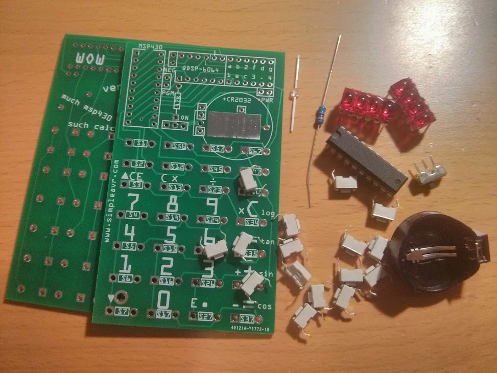
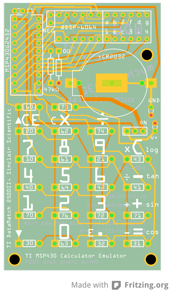
I had included the PCB designed here. I used Fritzing to do the PCB layout but it is thru-hole and simple enough that you can use any available PCB design software to do it.
For the parts,
- 1 x MSP430G2402, or another other MSP430G2xxx that is 20 pin DIP and at least 8K Flash
- 2 x bubble led, from Sparkfun
- 19 x tactile buttons, 6 x 3 x 4.3mm, thru-hole or smd both works
- 1 x spdt dip size switch
- 1 x CR2032 cell holder, thru-hole or smd pin to pin has to be 20mm apart
- 1 x miniature 1.8mm red led thru-hole
- 1 x 47k pull-up resistor
- 1 x 0.1uF by-pass capacitor
The miniature red led is to show the "negative" sign. The original calculators have 9 digit displays, since we have only 8 digit, I used a led to show the negative sign when needed.
You can try different CR2032 cell holders, or even paper-clip diys, the pcb make provisions to mount different cell holders.
General Assembly
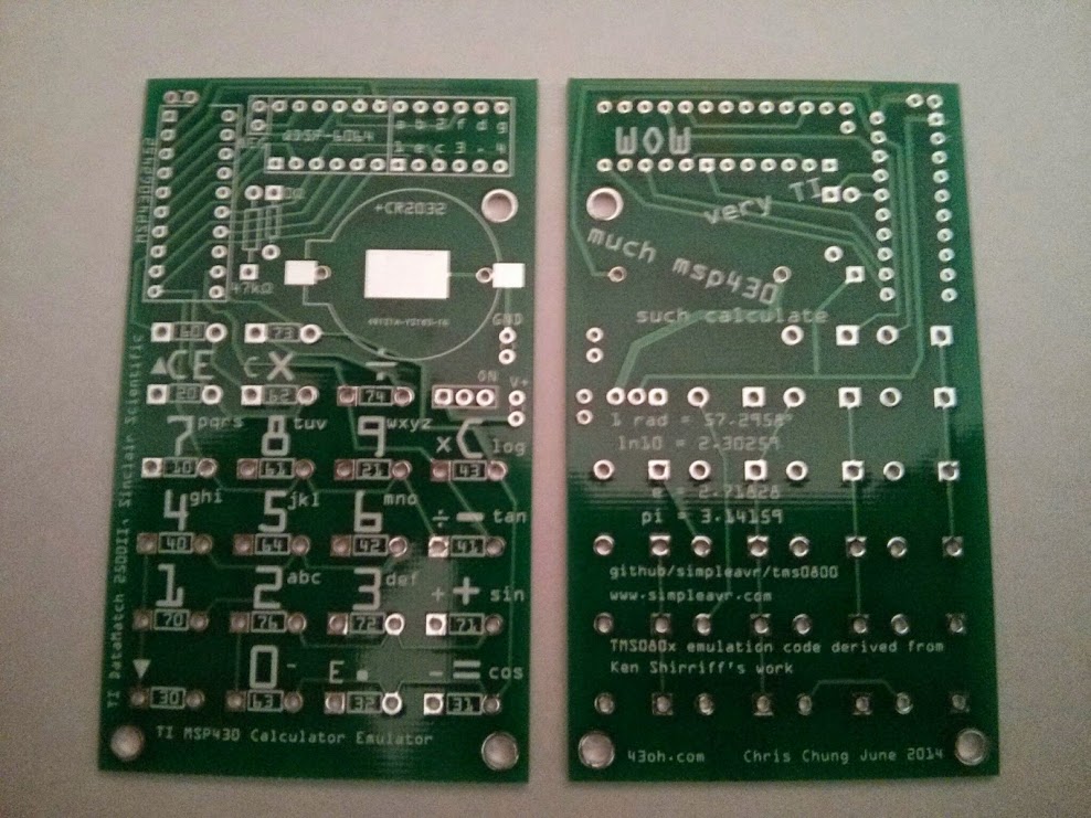
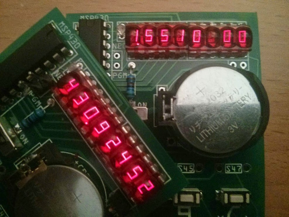
- Make sure you got the orientation of the msp430 mcu and led modules right. Square pads means pin 1. Dots on ICs and display modules means pin 1. Match them up.
- You should use a temperature controlled iron w/ clean (as clean as u can clean them) tips. * this tip in fact applies to all projects, also heat the component, not the solder. You will get clean joints that lasts.
- I don't think it matters too much, but I would place, solder components based on their difficulty. So if there is a certain part that you find challenging (say negotiating the part, your iron, etc), do that one 1st. You should try to fit all components w/o attempt to solder and gauge which ones should go 1st. My order is battery holder, tactile buttons, leds misc and mcu last.
- Some components are loose on their holes, you may want to use tape and or blu-tack to temporary secure them for soldering.
- If you don't think you need to re-program the firmware, you can skip the 0 ohm bridge and the Gnd, Vcc loop bridge. They are for hooking up to the programmer.
Schematic, Source Code and Build Hints
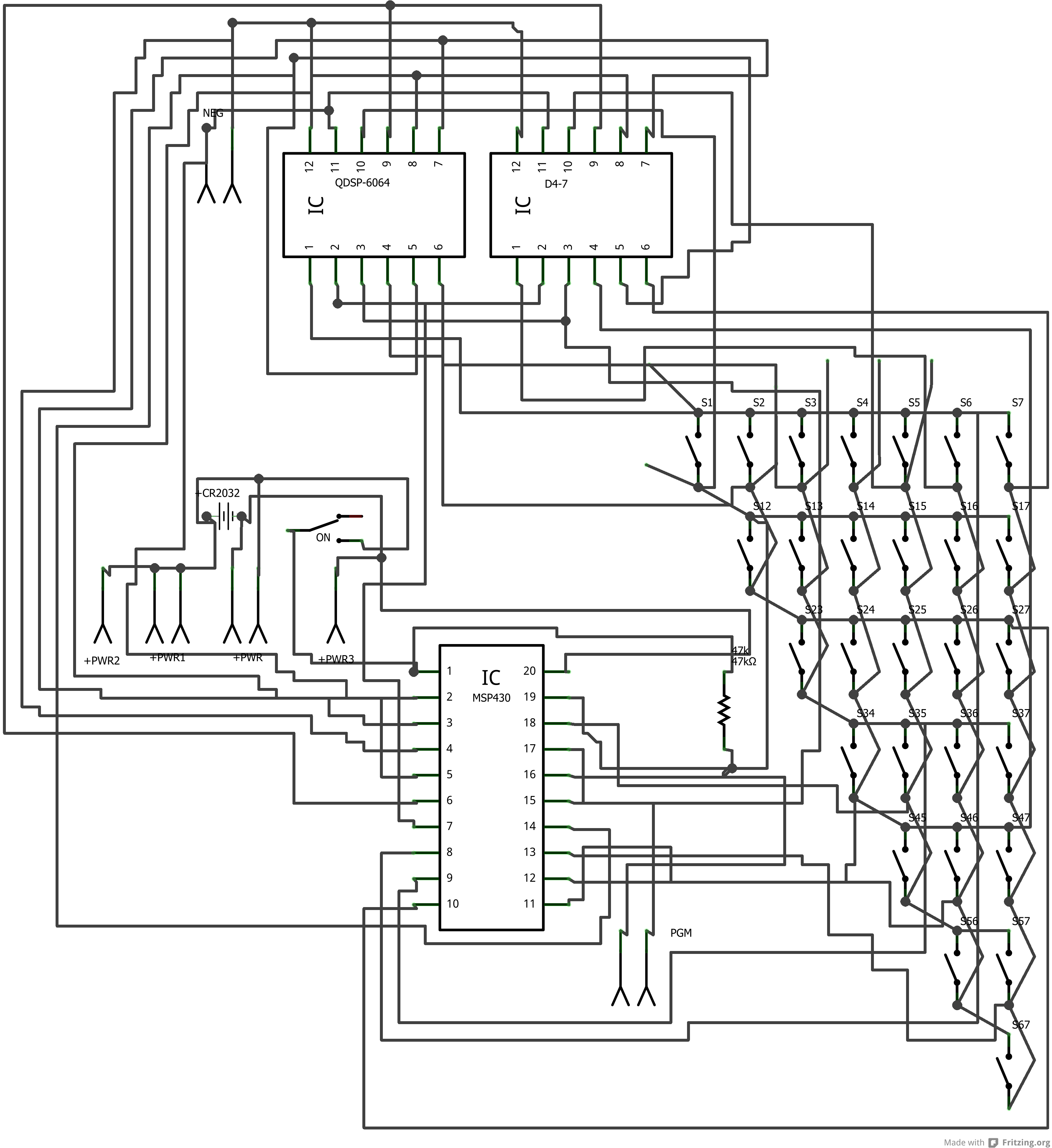
I am attaching the schematic here but it is not very readable, I started my pcb design by placing components 1st, make traces. And lastly I let Fritzing to auto route the schematic.
It is easier to understand the connections w/ the ascii art schematic, in my opinion
MSP430G2452

             -----------------
         /|\|                 |
          | |                 |
          --|RST              |
            |                 |       2 x 4 digit bubble led
            |     digit 0 P2.0|----- +---------+ +---------+
            |     digit 1 P2.6|----- | % % % % | | % % % % |
            |     digit 2 P2.1|----- +---------+ +---------+
            |     digit 3 P2.2|--/
            |     digit 4 P2.3|--/
            |     digit 5 P2.7|--/
            |     digit 6 P2.4|--/
            |     digit 7 P2.5|--/         segment a to g + dot........
            |                 |       /                                 ....\
            |                 |      /                                       \ (minus led)
            |   segment A P1.2|-----+-----+-----+-----+-----+-----+-----+-----+-(>|)-+
            |                 | _=_ | _=_ | _=_ | _=_ | _=_ | _=_ | _=_ | _=_ |      |
            |   segment B P1.3|-o o-+-o o-+-o o-+-o o-+-o o-+-o o-+-o o-+-o o-+-------
            |                 | _=_ | _=_ | _=_ | _=_ | _=_ | _=_ | _=_ |
            |   segment c P1.7|-o o-+-o o-+-o o-+-o o-+-o o-+-o o-+-o o-+
            |                 | _=_ | _=_ | _=_ | _=_ | _=_ | _=_ |
            |   segment D P1.1|-o o-+-o o-+-o o-+-o o-+-o o-+-o o-+
            |                 | _=_ | _=_ | _=_ | _=_ | _=_ |
            |   segment E P1.5|-o o-+-o o-+-o o-+-o o-+-o o-+
            |                 | _=_ | _=_ | _=_ | _=_ |
            |   segment F P1.4|-o o-+-o o-+-o o-+-o o-+
            |                 | _=_ | _=_ | _=_ |
            |   segment G P1.0|-o o-+-o o-+-o o-+
            |                 | _=_ |
            |   segment H P1.6|-o o-+       (not all buttons populated)
            |                 |
The TMS0803/0805 emulation logic has been adopted from Ken Shirriff's (plus others) web based emulators, TI and Sinclair Scientific.
There is also good amount of H/W information commented inside the code
If you plan to design your own PCB, the basic principle in relationship w/ the code is
- P1 for LED segments
- P2 for LED digits
- P1 also for key button scanning
You can move things around as long as you observe the above. I.e. If it fits better on your PCB, you could swap digit 1 w/ digit 3, segment A w/ segment E, etc, etc. All you need is to change #define in a header file and compile.
Bubble LEDs, Battery Holders and Buttons
Bubble LEDs
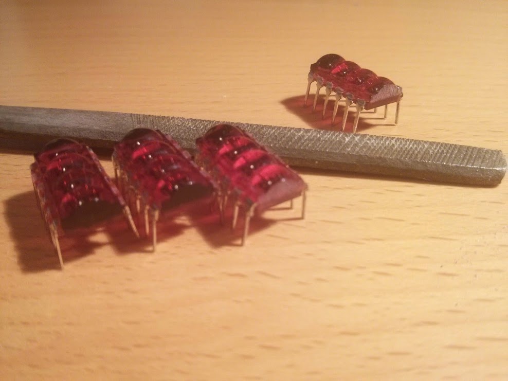
The two led modules are a very tight fit against each other. And when you force them down into positions one or both may have a tendency to get loose and rise from the PCB. After doing 2 boards, I start to file down the contacting sides of the modules.
This helps them fit better w/o grinding into each other. As a side note, I also noticed that by removing the black paint on the adjacent edges allow lights to pass through, thus when the display is on you won't see too much of a "blocking" line between the 4 digits. You can see the two displays on the right have been filed down on one of their edges. Also the black paints were removed.
* Also make sure you position your LED modules correctly. Pin 1 should be at SW corner, the pad is a square pad on the PCB and there is a black dot on the LED modules (underside) to indicate Pin 1.
Battery Holder
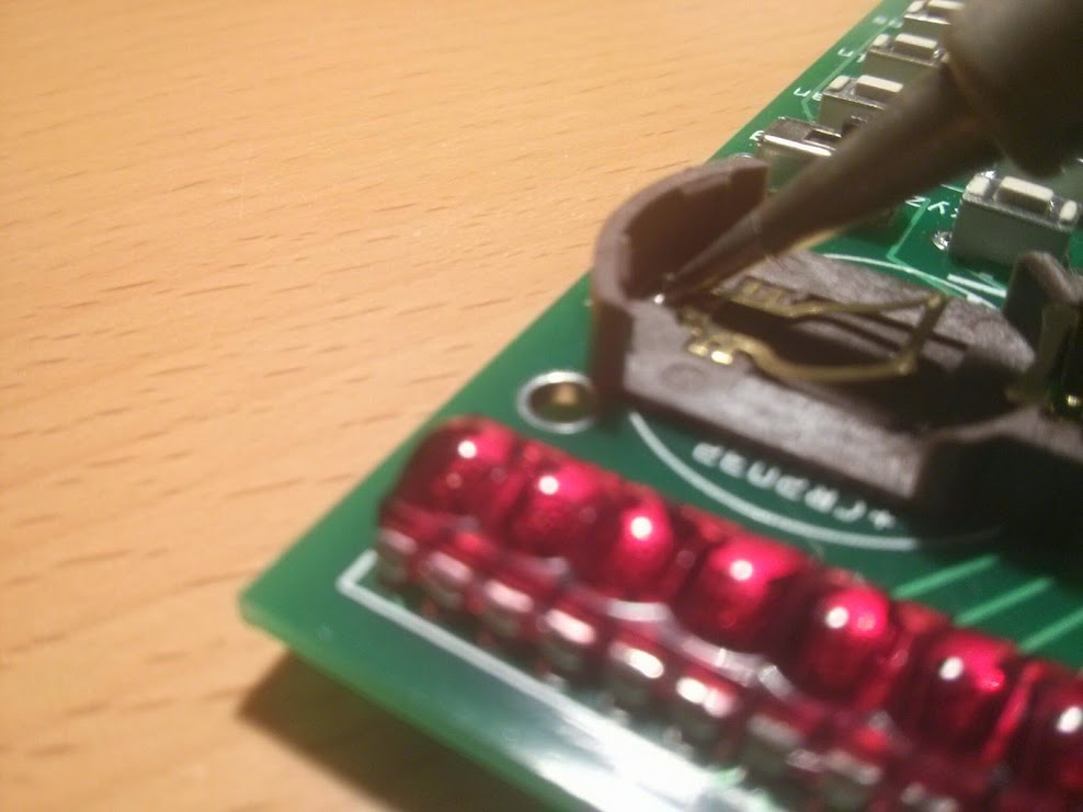
The PCB can accept both thru-hole and certain kind of smd battery holders. For the smd type that fits (pin to pin at 20mm), you should use solder paste to make one side of the join. If you do not have, I would tin both the PCB pad and the contact 1st, then turn up my iron and heat thru from the top of the smd contact to make the join.
Tactile Buttons
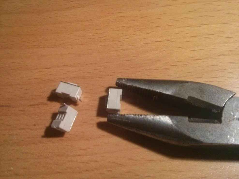
If you are using smd tactile buttons, you need to use long nose pliers to clamp the contacts into short pins.
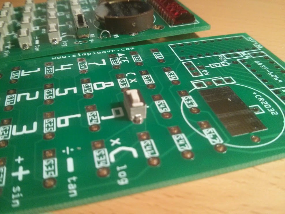
For both smd and thru-hole buttons, it is easier to solder on the top, one pin at a time, lay out a full column of buttons at a time, then solder one side of pins. Continue w/ the other 3 columns. With all buttons have one pin soldered, check for alignment and use iron + tweezer to adjust. Finally solder down the other side of pins for all buttons. When soldering, if needed you can use finger / tweezer to help secure position. The fit between the buttons and the holes are mostly ok. Unless your iron is not clean and you need to push around too much.
In-circuit Programming
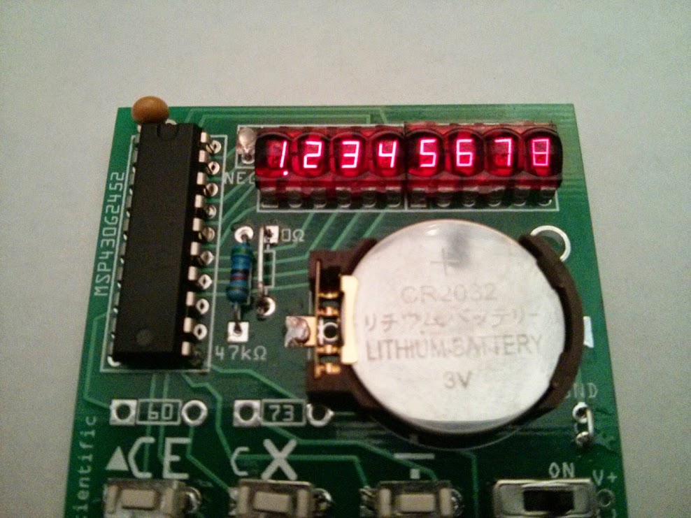
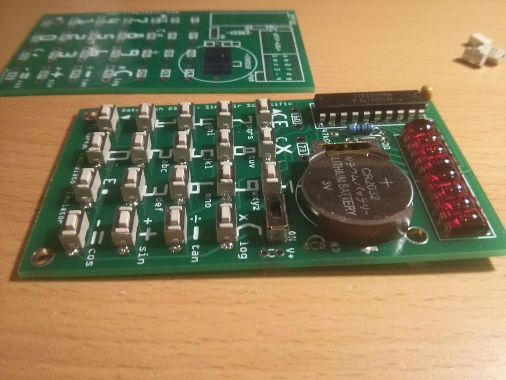
It is best to pre-program the MSP430G2xxx mcu before soldering it on to the PCB. And if there is any change to the firmware you can always re-program the mcu. We are not covering the programming of MSP430 here but should you require such information, they can be obtained easily from the web.
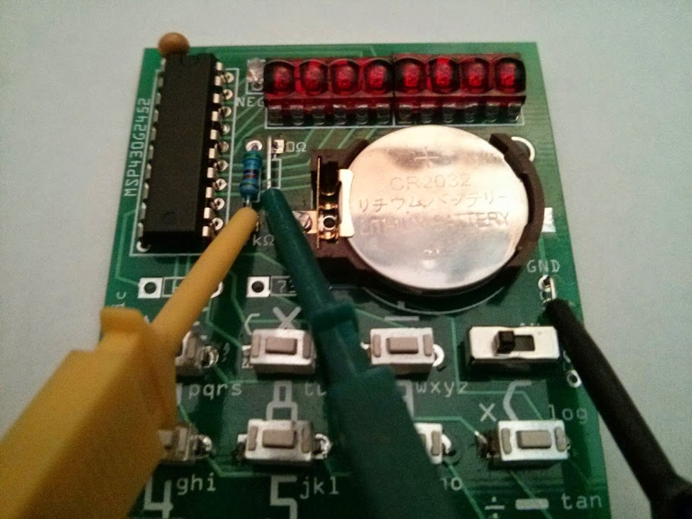
During development, I had used the TI Launchpad G2 to program the mcu. For in-circuit programming, the PCB had been designed to hook-up via IC hooks / clips. Show on the photo, the yellow hook goes to the LP-G2's RESET line, the green hook goes to the TEST line. The black hook just connect both grounds together. For a 3 line hookup, you still need to supply 3V power via the button cell during programming.
* Please note that the photo was done to show and is not 100% accurate, the yellow hook SHOULD connect to the TOP of the resistor.