Turn Your EAGLE Schematic Into a PCB
859456 Views, 613 Favorites, 0 Comments
Turn Your EAGLE Schematic Into a PCB
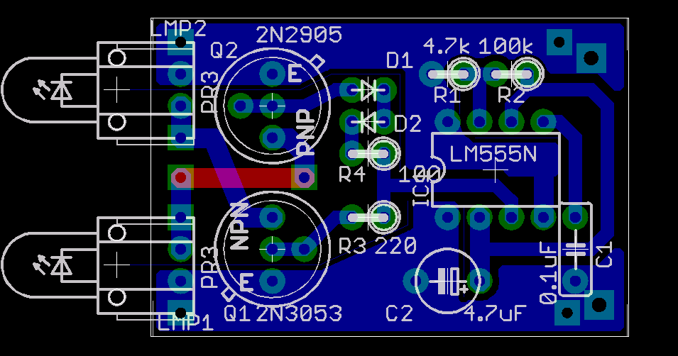
In a previous Instructable, I provided an intro to schematic entry using CadSoft's EAGLE editor.
In this instructable, we'll make a printed circuit board from that schematic
I guess I should say that we'll make a PCB DESIGN; making the physical board is a different task, and there are a lot of tutorials on the net (and even some instructables) on making the board after you have the design.
Cadsoft EAGLE is available from http://www.cadsoftusa.com/
Cadsoft is a German company that is a veritable mecca of software distribution enlightenment. In addition to the reasonably-priced professional PCB design packages ($1200), they have freeware, lite, non-profit, and other intermediate licenses. Their software runs under windows, linux, and MacOSX. It's slightly quirky, with a steep (but not too high) learning curve on the front end, but from most reports it is not any more so than other professional CAD packages. They have online support forums that are active from both the company and other users, the package is under current development and gets better with each release. A number of PCB fabricators will accept their CAD files directly. It's good stuff.
Use it. Propagate it. Buy it when you "go pro."
See also:
Schematic Entry
Creating Library parts
Design rule modification
Send CAD Files to manufacturers
In this instructable, we'll make a printed circuit board from that schematic
I guess I should say that we'll make a PCB DESIGN; making the physical board is a different task, and there are a lot of tutorials on the net (and even some instructables) on making the board after you have the design.
Cadsoft EAGLE generic information:
Cadsoft EAGLE is available from http://www.cadsoftusa.com/
Cadsoft is a German company that is a veritable mecca of software distribution enlightenment. In addition to the reasonably-priced professional PCB design packages ($1200), they have freeware, lite, non-profit, and other intermediate licenses. Their software runs under windows, linux, and MacOSX. It's slightly quirky, with a steep (but not too high) learning curve on the front end, but from most reports it is not any more so than other professional CAD packages. They have online support forums that are active from both the company and other users, the package is under current development and gets better with each release. A number of PCB fabricators will accept their CAD files directly. It's good stuff.
Use it. Propagate it. Buy it when you "go pro."
See also:
Schematic Entry
Creating Library parts
Design rule modification
Send CAD Files to manufacturers
Starting From the Schematic...
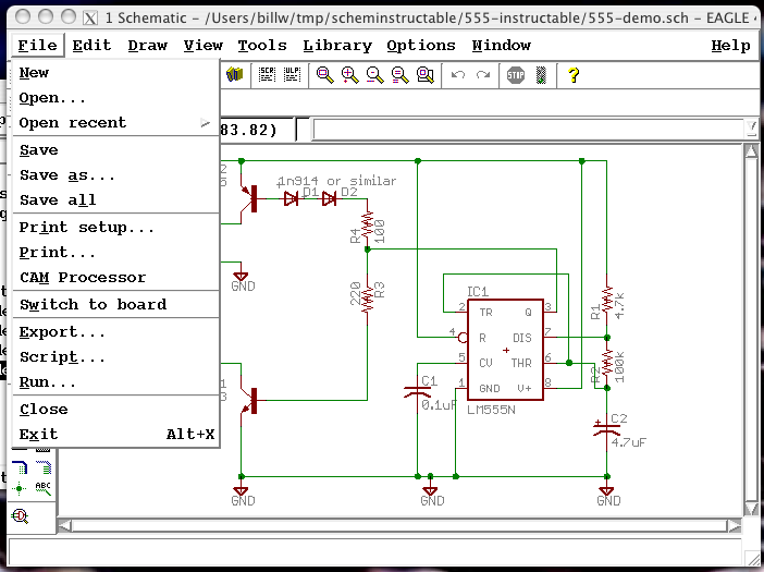
So this is the schematic we have from the Schematic Instructable. Up in the file menu, there's a "Switch to board" selection. If we do that from a bare schematic, it will offer to create the board from the schematic for us (say "yes"), and then leave us sitting in the Board Editor.
Menu Commands Used
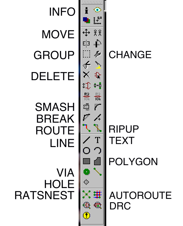
The Board Editor looks a lot like the schematic editor, with some different commands.
Here's a summary of the iconic commands that I use in this instructable, and some brief summaries:
INFO Shows information about an object (component, signal, trace, etc.)
MOVE Allows components to be moved (same as schematic.)
GROUP Groups a collection of objects into a "group" that can be manipulated simultaneously.
DELETE Delete an object. Items created in schematics need to be deleted there.
SMASH Separate the text labels of a part from the part itself, so they can be moved independently.
BREAK Add a corner to a line (or trace.)
ROUTE turn an airwire into a trace
LINE draw lines (usually in non-copper layers. ROUTE is for drawing copper.)
VIA create a hole and pad associated with some signal. (actually, we'll use a text command.)
HOLE a hole that isn't associated with a signal, ie for mounting.
RATSNEST recomputes airwires and polygons, eg after components have been moved.
CHANGE changes an object's properties.
RIPUP changes a routed trace back to an airwire. Sorta equivilent to "delete" for traces.
TEXT add text
POLYGON create a polygon (actually, we'll use a text command.)
AUTOROUTE invoke the autorouter.
DRC invoke the Design Rule Check and parameter setting.
I'll describe the remaining icons toward the end, and assign them "useful" or "useless."
The Untouched PCB Design
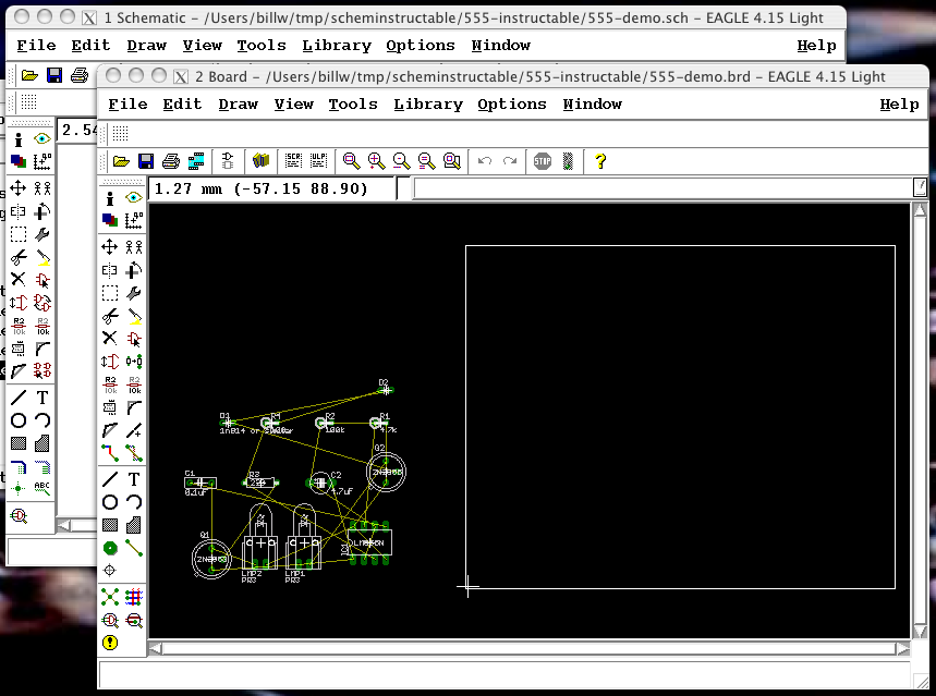
This is what the newly created board design will look like. All your components will be in a clump over to the left of the origin, and there will be a frame that marks the allowed size of a board when using the freeware or "Lite" versions of EAGLE (80x100mm). All the component pads will have to be inside that outline when you move them around, although you can cheat a bit and have traces or board outlines that exceed the board size limit. This has the annoying side-effect that if you pick up a component from it's original localtion, you can't put it back down outside the outline (however, you can use ESC to abort the move, and the component will revert to its original location.)
All the signals you created in the schematic are currently AIR WIRES; thin yellow lines that are drawn in the shortest possible way, crossing each other as needed. They stay connected to component pins even when you move the component around. The RATSNEST command recomputes and redraws these after you move things around (and, say, make two connected pins closer together than they used to be.)
ROUTING a signal consists of turning an airwire into an actual copper trace on some layer(s) of the board, and positioning that trace so that it doesn't short agains other traces on the same layer of the board. The Freeware version of Eagle only supports a TOP and BOTTOM layer, and as hobbyists we have motivation to try to use only ONE layer. A signal can transition from one layer to another using a via, which is a conducting hole, sorta like a jumper (and we'll use jumpers to implement the top level of the board if we can make the board mostly single-sided.)
Creating the PCB design consists of placing all the components in logical places, and routing all the airwires in a way that allows the design to work.
Ok, a few defintions are in order
All the signals you created in the schematic are currently AIR WIRES; thin yellow lines that are drawn in the shortest possible way, crossing each other as needed. They stay connected to component pins even when you move the component around. The RATSNEST command recomputes and redraws these after you move things around (and, say, make two connected pins closer together than they used to be.)
ROUTING a signal consists of turning an airwire into an actual copper trace on some layer(s) of the board, and positioning that trace so that it doesn't short agains other traces on the same layer of the board. The Freeware version of Eagle only supports a TOP and BOTTOM layer, and as hobbyists we have motivation to try to use only ONE layer. A signal can transition from one layer to another using a via, which is a conducting hole, sorta like a jumper (and we'll use jumpers to implement the top level of the board if we can make the board mostly single-sided.)
Creating the PCB design consists of placing all the components in logical places, and routing all the airwires in a way that allows the design to work.
About Board "layers"
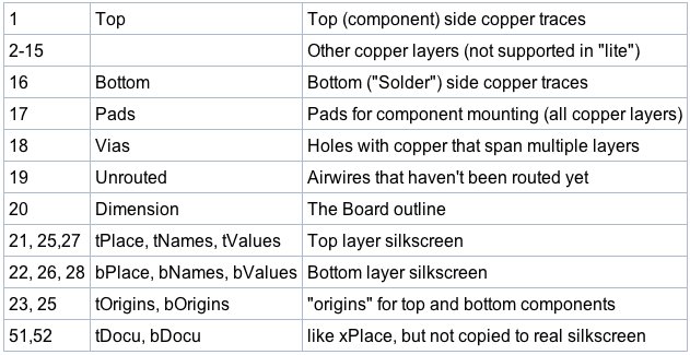
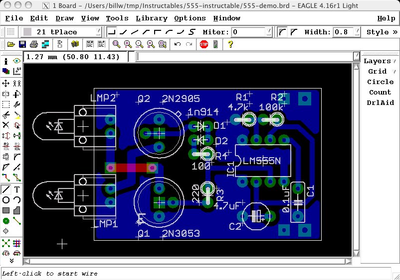

The Eagle Board editor has MANY more layers than the schematic editor. A confusing multitude of layers. Most of the drawing commands have a layer-selection pulldown menu that you can use for specifying which layer you want to draw on (exceptions include objects like vias that span multiple layers.)
Here are some of the more important layers:
Here are some of the more important layers:
Move the Components Into the Legal Area
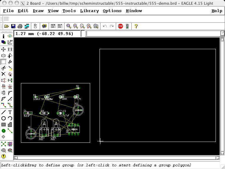
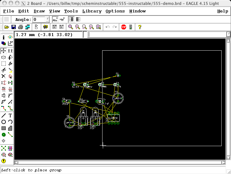
The first thing we want to do is move at least some components into the legal board area where we can work with them. If you have a particularly large board with many components, you might want to do this a section at a time. For this sample board, we have plenty of room and we can move them all at once, using the group-move feature.
Select the GROUP icon, then click and drag to make a rectangle that goes all the way around the components. Then select the MOVE icon and RIGHT click (right clicking selects the group instead of a single component) and drag the set into the board outline. Use the ZOOM button to tighter the view.
Select the GROUP icon, then click and drag to make a rectangle that goes all the way around the components. Then select the MOVE icon and RIGHT click (right clicking selects the group instead of a single component) and drag the set into the board outline. Use the ZOOM button to tighter the view.
Shrink the Boad Outline a Bit
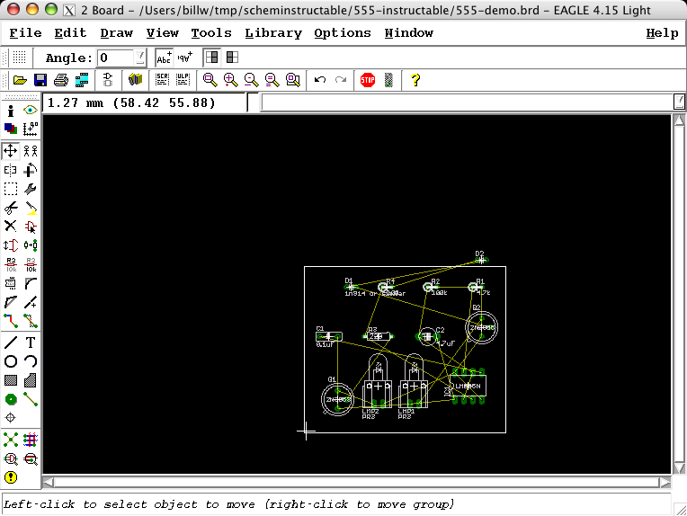
The full legal side of the board is bigger than we need. Shrink the outline by using the MOVE tool. Click on the center of the top horizontal line (which selects the whole line instead of an endpoint) and move it down, Then click on the center of the rightmost vertical line and move it leftward.
Clicking near the center of a line moves the whole line. Clicking near a vertice moves only the point.
It doesn't have to be perfect at this point; we're mostly looking for a better view for the next steps. (Oh yeah - click the zoom button to re-zoom the window on the smaller outline.)
Clicking near the center of a line moves the whole line. Clicking near a vertice moves only the point.
It doesn't have to be perfect at this point; we're mostly looking for a better view for the next steps. (Oh yeah - click the zoom button to re-zoom the window on the smaller outline.)
Start Placing the Components
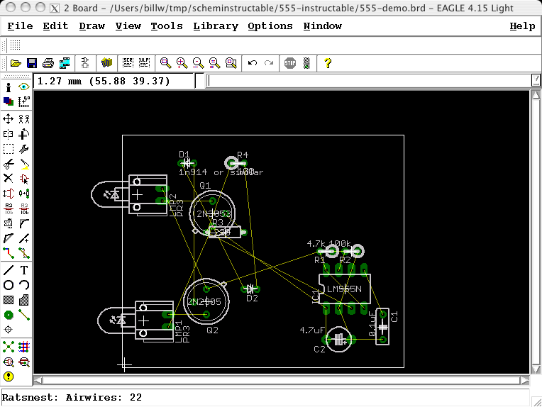
Now we need to move the components to (near) where we want them on the final board. OR we want to move them to sensible places that will make the placement of traces easier. A lot of the "ART" of making PCBs (and especially Single Sided Boards) lies in finding "good" places for the components.
In general, you can start by placing the components similar to how they appear on the schematic. (This breaks down when a chip has multiple gates, or the diagram in the schematic symbol has vastly different pinn placement than the actual chip, but it's a good place to start for discreets and simple components. The worst that will happen is that you'll have a layout that makes sense, even if it doesn't route well...)
In this case, I put the power output transistotrs near lamps that they're associated with, and I looked on the web for a 555 layout that would work well (for the longest time, I tried to do boards with the timing cap placed near the timing resistors, and I always needed a jumper. Sigh.) ("Let no one else's work evade your eyes.")
Check Signals to See How They'll Route

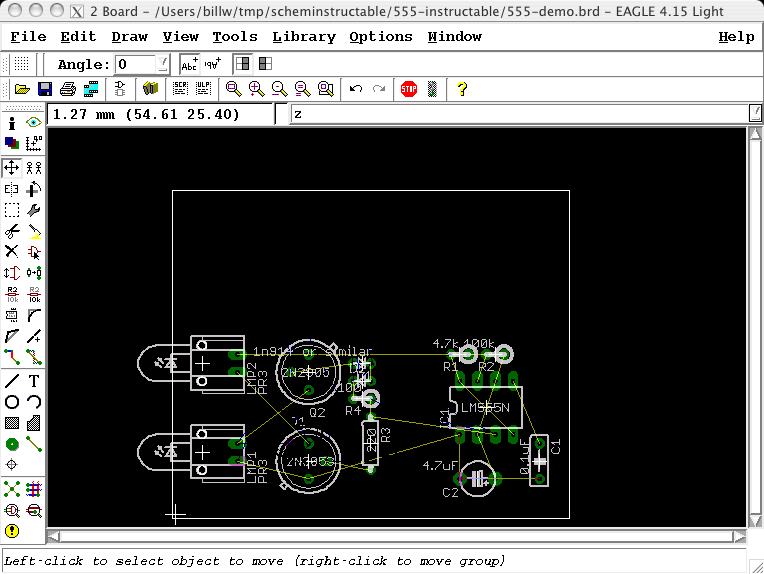
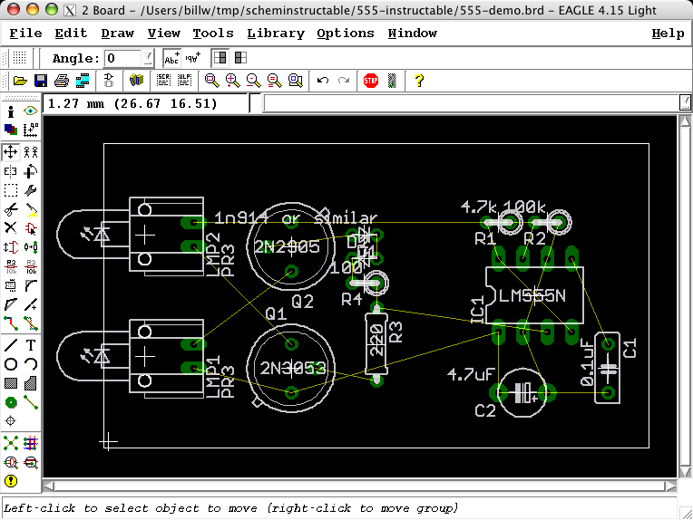
One way to get hints on part placement is to look at some significant signals to see whether they have nice straight paths, or whether they zigzag all over the board. First use the RATSNEST icon/command to have EAGLE recompute the airwires. The way things are now, I have nice straight connections from the transistors to the lamps, but if I type "show gnd" in the command line, I see that this is at the expense of making the ground signal zigzag. So I swap the transistors because GND is more important to have straight. (IMHO, YMMV, etc.) (This ends up putting the transistors near the supplies that they switch, rather than near the lamps that they switch to, so that still makes sense from a circuit point of view too.)
After the rest of the components are placed in ok-looking relative locations, I can squeeze them together again (manually, moving them one at a time; no magic command for this!) and shrink the board outline some more.
After the rest of the components are placed in ok-looking relative locations, I can squeeze them together again (manually, moving them one at a time; no magic command for this!) and shrink the board outline some more.
Load Design Rules
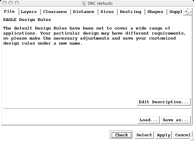
Since we're hobbyists, we want to make our board with wide traces and big spaces (see https://www.instructables.com/id/EZVIGHUBGCEP287BJB/ )
So we'll load up that set of hobbyist design rules before we start laying out tracks.
Click the Design Rule Check icon and use the LOAD button to load hobby.dru from my other instructable. Or you can modify values manually and individually, of course. Or leave them as is...
So we'll load up that set of hobbyist design rules before we start laying out tracks.
Click the Design Rule Check icon and use the LOAD button to load hobby.dru from my other instructable. Or you can modify values manually and individually, of course. Or leave them as is...
Fix Incorrect Package
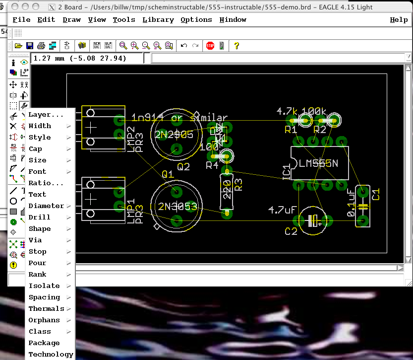
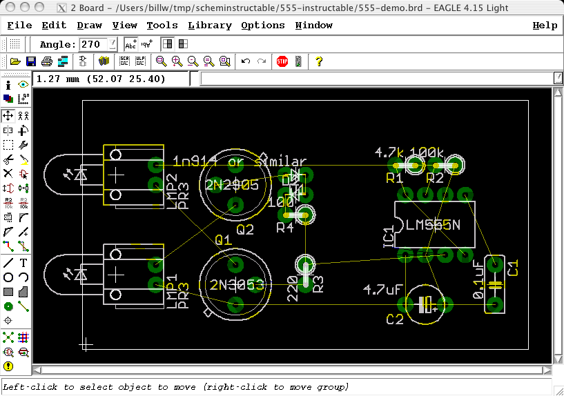
You can see how the design rule change has already modified the board. Pads are bigger, and they're all round.
You'll also notice that one of the resistors is set as a non-vertical package, unlike the rest. This was probably an error in the schematic entry, and it didn't matter when all we had was the schematic. Now that we are making the board, we want to change the package as appropriate.
When you select the change->package tool and click on the part to change, you'll be shown a list of all the legal packages for that part (these should be the same ones that showed up in the schematic "add" dialog)
There are other ways to enter a "change" command in the text command entry area that you'll want to look into if you need to change a lot of devices to a particular package, so you can skip going through the list for each one. Something like "change package 'R-US/0207/2V', and then just click on each component.
Try the Autorouter

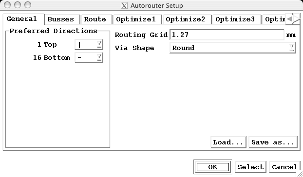
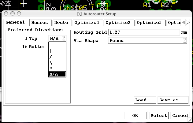
Now we'll see if the autorouter can do some of the work for us. The EAGLE autorouter isn't the best in the world, but even when it does a "bad" job, it will give us some general hints on how things need to look, or where the trouble spots are.
Clcik the AUTOROUTE icon, and a dialog box will pop up. The default parameters will produce a double sided board, and we want to at least TRY to make a single-sided board, so the first thing to do is set the preferred direction for the TOP layer to NA (Not Applicable.)
The other thing you may need to change is the routing grid. This defaults to the same default grid as the board layout editor in general: 0.05 inches (1.27mm, since I have my editor set up in metric.) Since this particular board has big parts, and we haven't moved any off the default grid, we're ok with that value. If you have SMT components or have moved things around on a finer grid, you might have pads that are not on the touing grid, which the autorouter doesn't like much ("unreachable pad", etc) You can make the grid very small, but it will take longer. IMO, it's better to start with a coarse grid and halve it each time it looks like routes fail because the grid is too large.
Also note that the autorouter obeys the board dimension lines, so if you haven't moved them close to your components, you might have traces travel all over the board. Or if you've moved the outline too close to the pads, you may have prevented traces from going places they need to go.
Route Remaining Tracks Manually
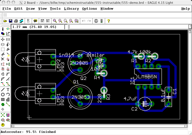
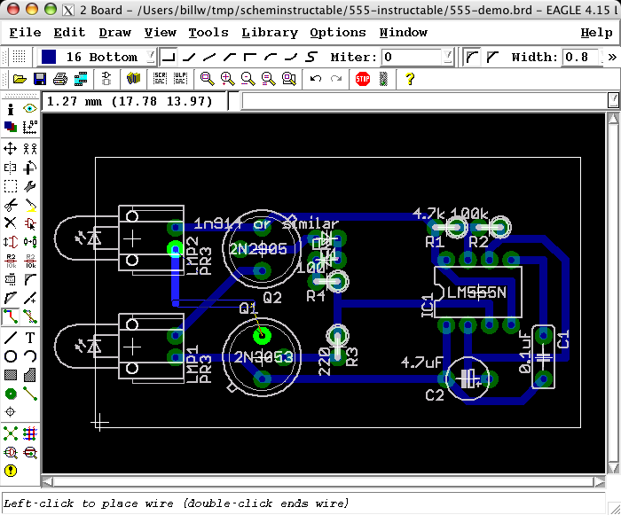


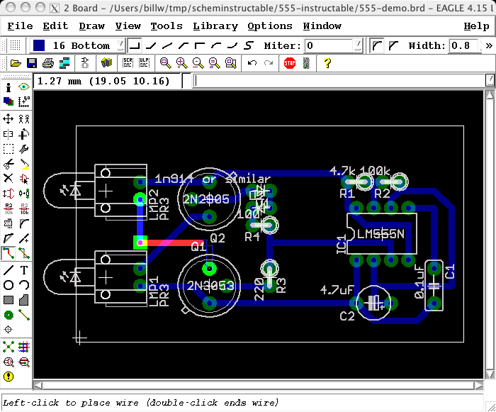
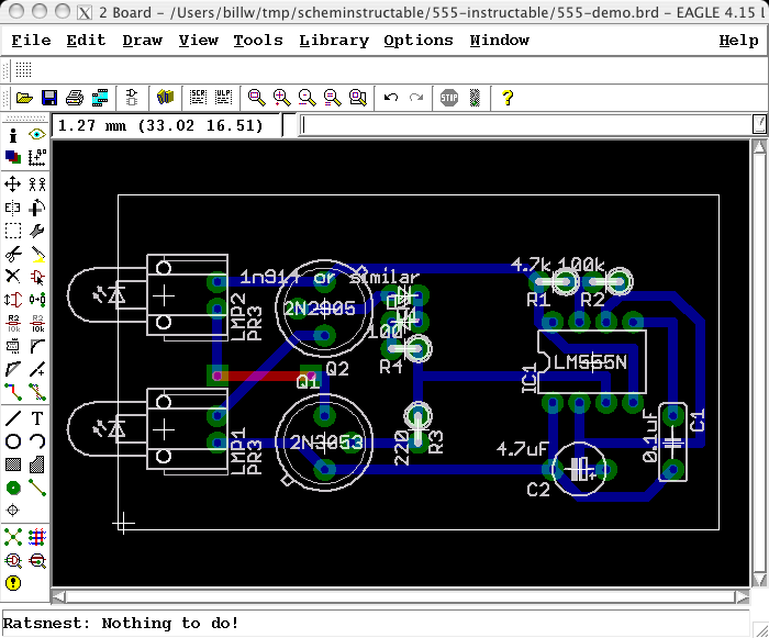
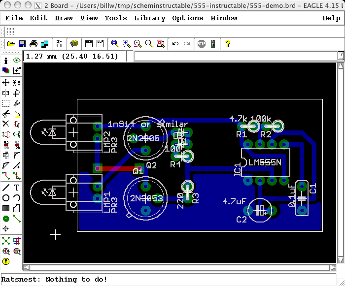
The autorouter did a pretty nice job here. There's only one trace left.
There are a couple of ways we could route this signal manually, including some snakey routes between transistor pins that the autorouter didn't use because of the design rules we specified. This is a relatively high current trace, and I decided that I won't manually violate the design rules either. Instead, I'll use a jumper wire on the component side, which I can model in EAGLE as a top-side trace.
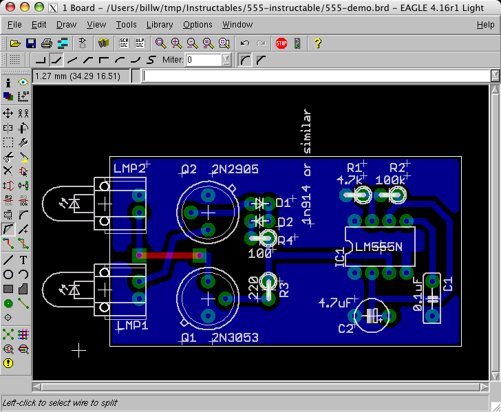
Select the ROUTE tool and click on an endpoint of an unrouted (yellow) airwire, and you can position a trace pretty much anywhere you want, selecting width, layer, and type of bend from the menu bar as you go along. This is shown in the succession of pictures in this step.
Add Power Plane Polygons
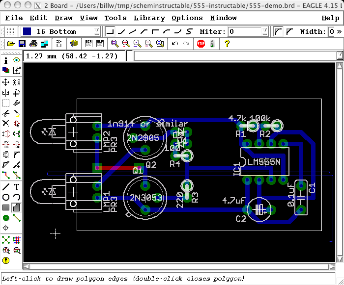
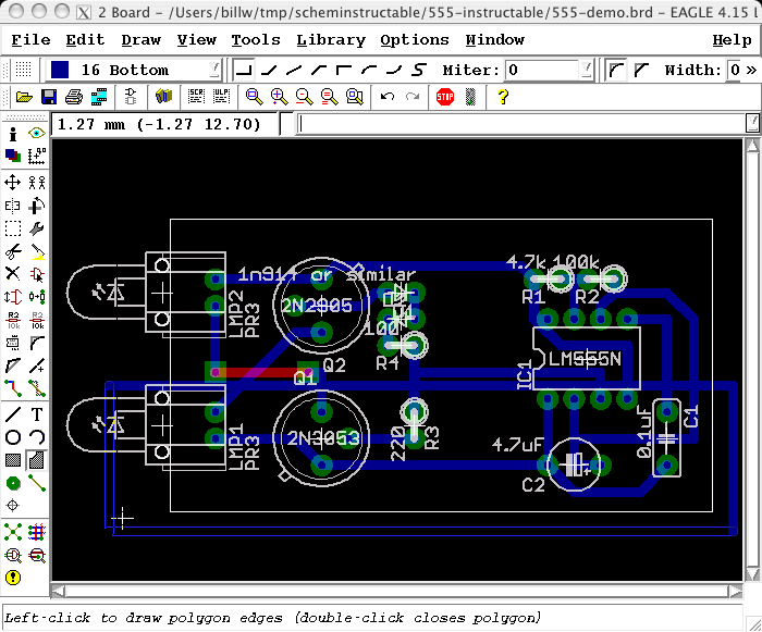
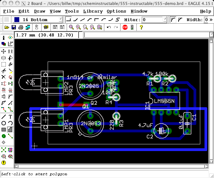
"Power planes" are large areas of copper that carry an actual signal, usually power and ground. On multi-layer boards, it's common to have entire layers mostly dedicated to such a power plane. Even on a single layer board there are some advantages to doing something similar:
1) Use less etchant
2) carries heavier current, just in case
3) makes it easier to attach test leads
4) acts as a sort of "static barrier" to fingers
In EAGLE. such large signal areas are drawn with the "polygon" command. There is an icon on the toolbar for drawing polygons, but it will create polygons associated with a new signal, and I find that when creating a polygon for an existing signal, it's easier to type the text form of the command in the text command area. To create a polygon attached to a signal named 'gnd', type "poly gnd" By giving it a signal name in the command, the polygon will automatcailly be connected to that signal. (If you draw a polygon with the icon, you can connect it to a signal later by using the "name" command to rename the polygon. (however, after this, you can't rename the polygone again without renaming the signal as well.))
Add V+ Polygon
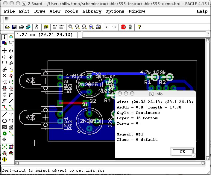
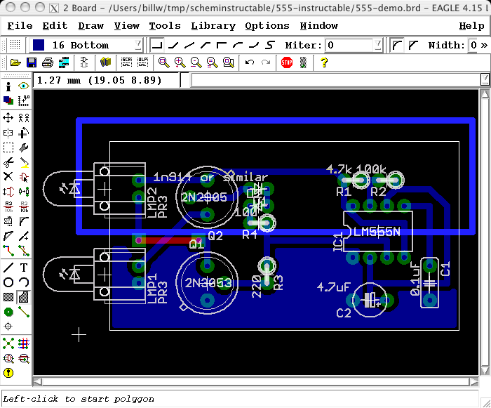
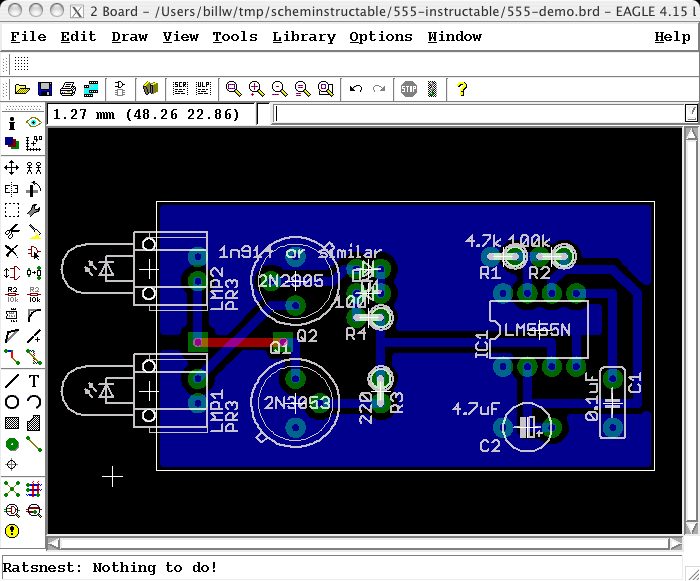
Now we'll repeat the process for the positive voltage. However, we never named that signal when we drew the schematic, so it will have some random name like "N$23"; We can use the "INFO" command to find the signal name to use when we draw the polygon, after which it's the same as drawing the GND polygon.
In this case, the V+ signal is named n$1, so we type "poly n$1"
In this case, the V+ signal is named n$1, so we type "poly n$1"
Neaten Up: Smash Package Text
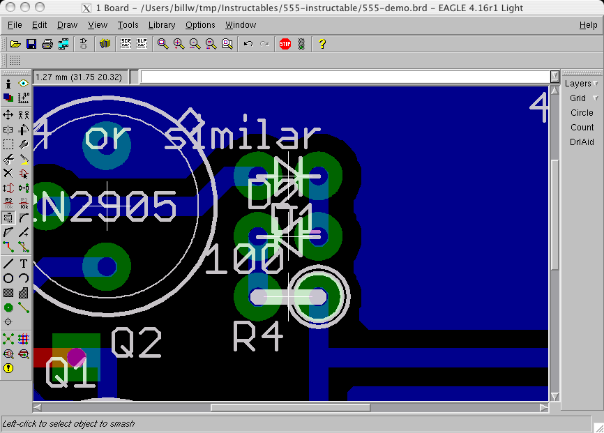
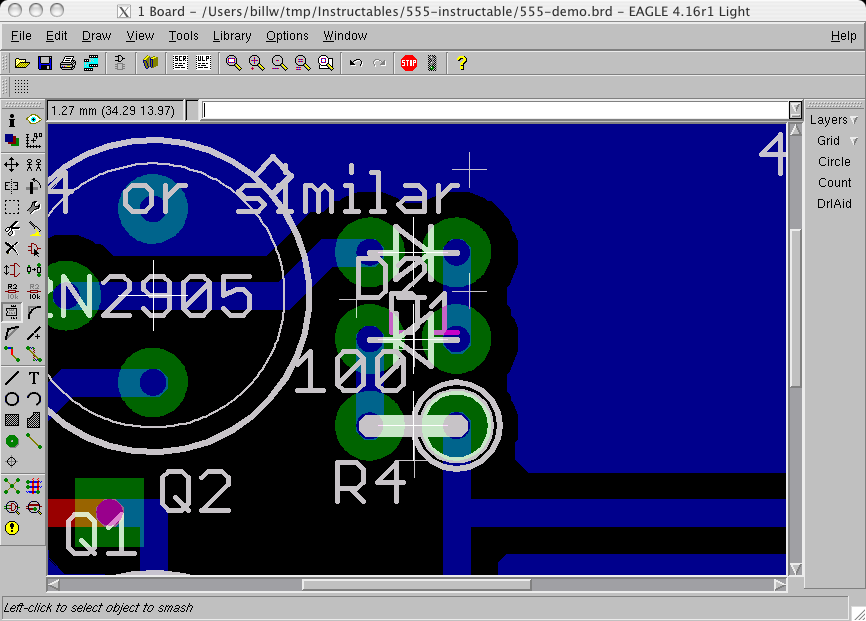
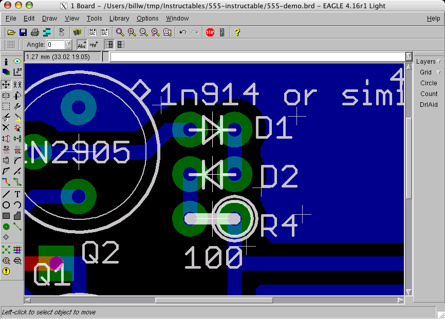
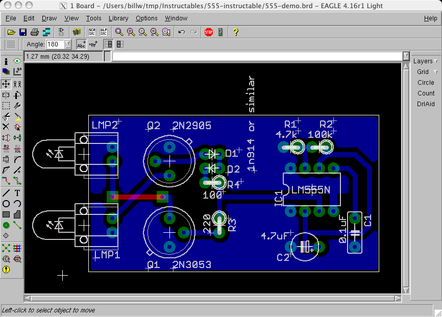
If we want the names of components to be legible on the top of the board (transferred via toner transfer), or just to look good on printouts, they names and values probably have to be moved from their default locations. In order to move the text separately from the device itself, we use the "SMASH" command. (Why is it called "smash" ? I dunno!)
Select the SMASH icon from the menu, then click each component whose text you want to move. If this is ALL of the components, there's a ULP that will smash everything (but ULPs are a subject for possible future instructables. Or the EAGLE manuals.)
Select the SMASH icon from the menu, then click each component whose text you want to move. If this is ALL of the components, there's a ULP that will smash everything (but ULPs are a subject for possible future instructables. Or the EAGLE manuals.)
Neaten Up; Move Traces


We can move some of the traces so they look neater, offer better clearance, etc.
Also, we shrink the board to its final size ny squishing the components together some more.
Also, we shrink the board to its final size ny squishing the components together some more.
Fixing an OOPS!

Remember back in the schematic I mentioned that there were a couple of things that had been left out? You should be noticing them about now...
POWER connections; there's no way to connect a battery or power supply to this circuit board. Oh sure, you can just tack some wires onto the supply polygons, but how elegant is that!
We could go back to the schematic and add some actual power connectors or battery holders, but those are a bit rigid for a circuit that's probably going to be connected to a battery pack with some wires anyway. Instead, let's add some Vias to act as connection points for the power wires.
When adding Vias like this, it is convenient to use the text command entry area so we can name the signal at the same time we add the via. Type "via 'gnd'" (yes, you need the quotes here, unlike for polygons.) You can adjust the drill size and via shape, and plunk the via down in the appropriate supply polygon. I like to use two vias as a sort of strain relief (one is made larger so you can feed wire + insulation through it, the other is sized for just the wire.) A click on the RATSNEST icon will make sure the vias are connected to the polygon. Then do the same for the V+ signal (named N$1, you recall.)
Neaten Up: Allow for Alternate Packages and Options


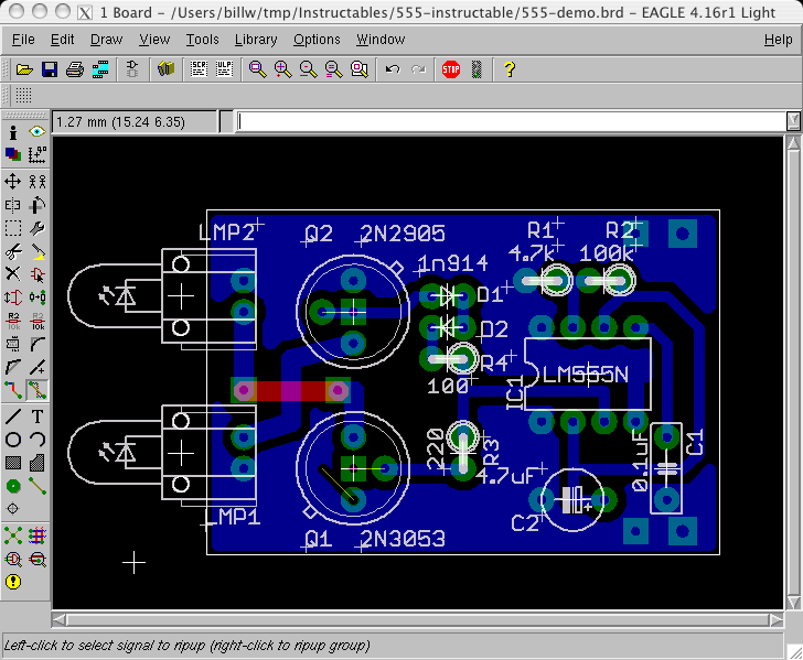
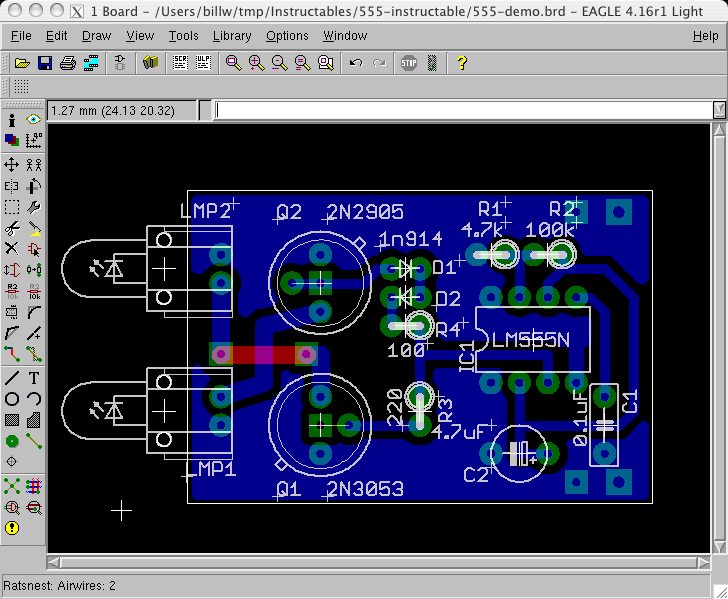
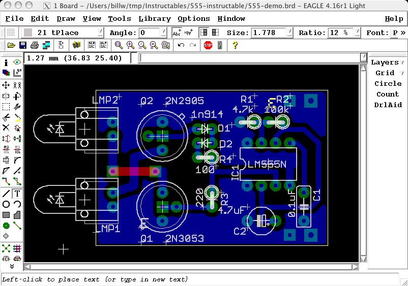
We can drop some extra holes for mounting different packages. The transistors used in the published schematic that we entered apparently come in a sort of metal can package that has dropped in popularity. If we arrange for three in-line mounting holes, we can substitute a whole lot of different transistors whose package leads come that way (TO92 or TO220, to mention two popular modern packages.)
Use the info command to figure out the signal names, and then "via 'n$X'" on the command line to create the via, followed by a manual route to the via if needed. In this case, one of the vias placed collides with a signal trace hidden by the GND polygon, so we have to remove that trace with the "ripup" command (the polygon will still connect to the pad.)
While we're at it. I'll add some text to the silkscreen to show where the emitter lead of the transistors should go. Use the "text" icon button, and change the layer to tPlace.
Do Design Rule Check

We want to run a design rule check to make sure that none of the manual editing we've done violates the rules...
Output Using Exported Images

Save your work often. You've been doing that, right?
Now we're essentially done, and we should figure out how we're going to output our board for
admiration on web pages, review by peers, transfer to physical PCB material, and so on.
One way to output the board is to "export" an image.
Now we're essentially done, and we should figure out how we're going to output our board for
admiration on web pages, review by peers, transfer to physical PCB material, and so on.
One way to output the board is to "export" an image.
Other Useful Menu Icons
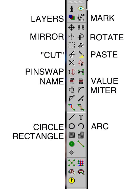
Here are some other useful commands accessible from the menu icons
LAYERS Adjust which layers are displayed. Boards have many more layers than schematics!
MIRROR Move a component from being mounted on the top of the board to being mounted on the bottom of the board.
CUT COPYS a selection, despite the name.
NAME Change the name of an object.
CIRCLE Draw a circle.
RECTANGLE Draw a rectangle.
MARK Place a measurement mark. Your info area will start showing distances relative to the mark as well as to the origin.
ROTATE rotate an object. This can rotate angles other than 90 degrees.
PASTE Paste some objects that were previously copied with CUT.
VALUE Change the value of an object.
MITER make signal corners rounded.
ARC Draw an arc.
Useless Commands
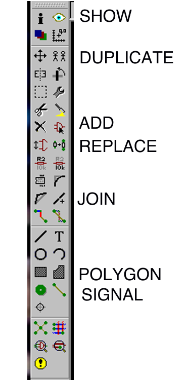
These are menu icons that I don't find at all useful in creating boards, at least not from schematics (and I feel that you should always make schematics to go with your boards; borh for self-documentation and the error-checking capabilities that are added.)
SHOW SHOW is more useful from the text command area. I think.
DUPLICATE Duplicate an object. Usually done in the schematic.
ADD Add a component. Usuaully done in the schematic.
REPLACE
JOIN Happens automatically, usually?
POLYGON more useful from the text command area.
SIGNAL Create a signal. Usually done in the schematic