Turn an Old Cellphone Into a Data Sending Device (using an Arduino)
by Monoclecat in Circuits > Electronics
59967 Views, 533 Favorites, 0 Comments
Turn an Old Cellphone Into a Data Sending Device (using an Arduino)
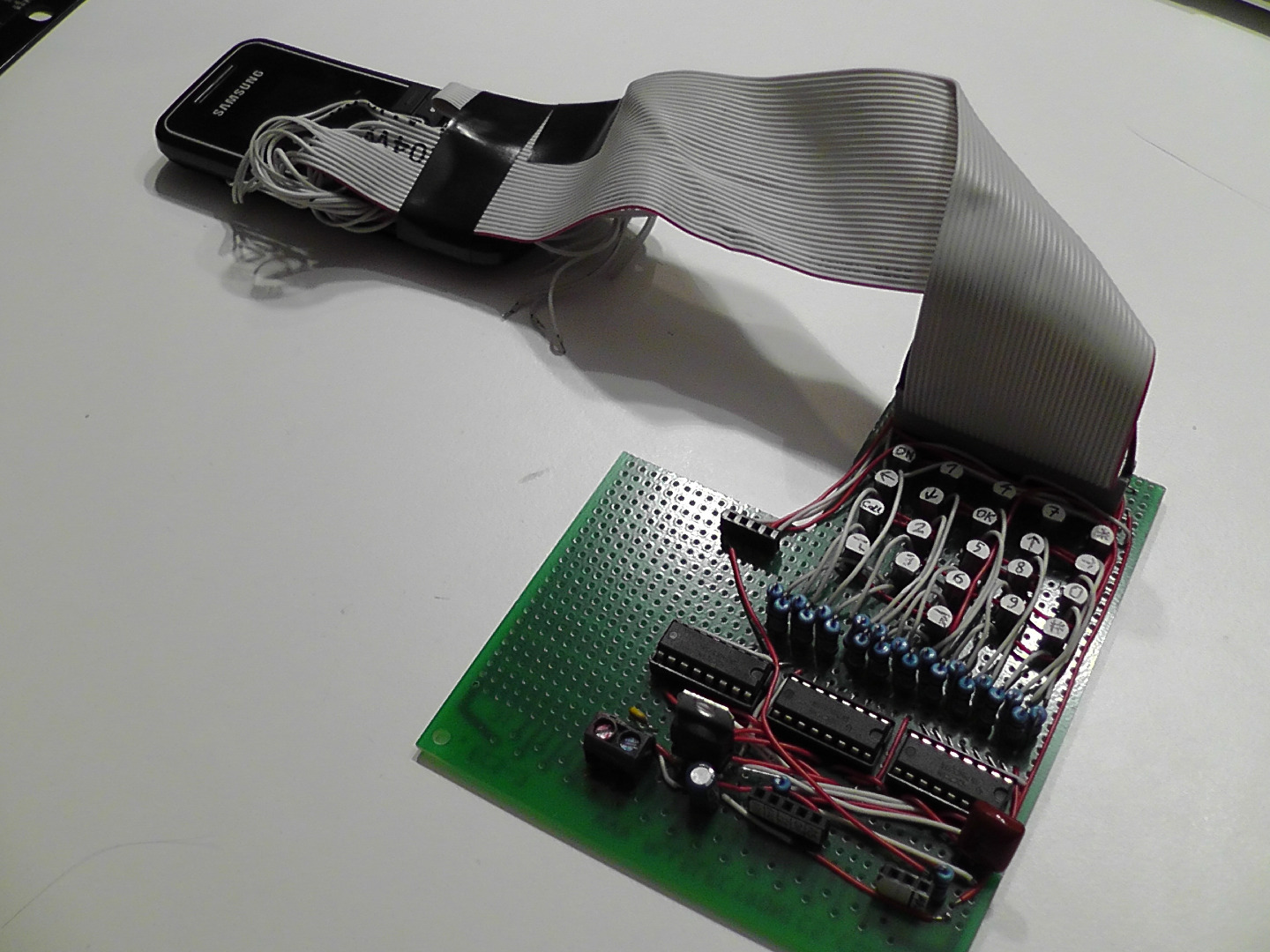
What will this device do?
When complete, the combination of circuitry, arduino and modded cellphone will be able to autonomously send data through texts via the cellular network. This could be sensor data, for example from weather sensors.
What am I going to show you in this tutorial?
In this tutorial I will show you how to mod an old cellphone and I will walk you through the soldering of the external circuitry. I will also explain the concept of the program for this application.
This instructable concentrates on the hardware for this to work.
What's a remote data sending device?
What I define as a remote data sending device is a gadget that can send data over a long distance when requested to do so.
How will this gadget do that? When you call the number of the SIM card you put in the cellphone, the phone will see an incoming call. The external circuitry will register you calling and will then abort the call (so you don't pay for a call). Then the microcontroller will take the data it collected and will write a text message using transistors soldered to the buttons of the keypad.
Why not buy a unit specifically built for this job or use a smartphone with an app that does the same?
Mainly because of the costs. A cellular shield for an arduino uno can easily rake $60 out of your budget. This cellphone hack will only cost you about $4, but will take a few hours to build. Any arduino board should work - I use an arduino uno in this project.
The cost of $4 is only for the electronics components if you already have an old phone (which cost around $20). Personally, I had old phones laying around that I didn't use anymore, so why not transform them into something useful? This way you are recycling old phones that would otherwise end up in the landfill.
The main disadvantage is the slow data sending rate. Basically, it's about twice as fast as you could do it by hand. The circuit directly 'presses' the buttons, which means you can do anything you could do by yourself. In this tutorial I will only concentrate on sending data from the device with text messages. With a bit of thinking, tinkering and additional circuitry you could even send data in form of frequencies in a call, but that would be an entire tutorial by itself.
Experience needed for this project:
- Experience with soldering circuits to perf boards
- Basic knowledge of how to get transistors to work
- Ability to read schematics
- Experience in the field of electronics in general
- Some basic programming knowledge
What You Need
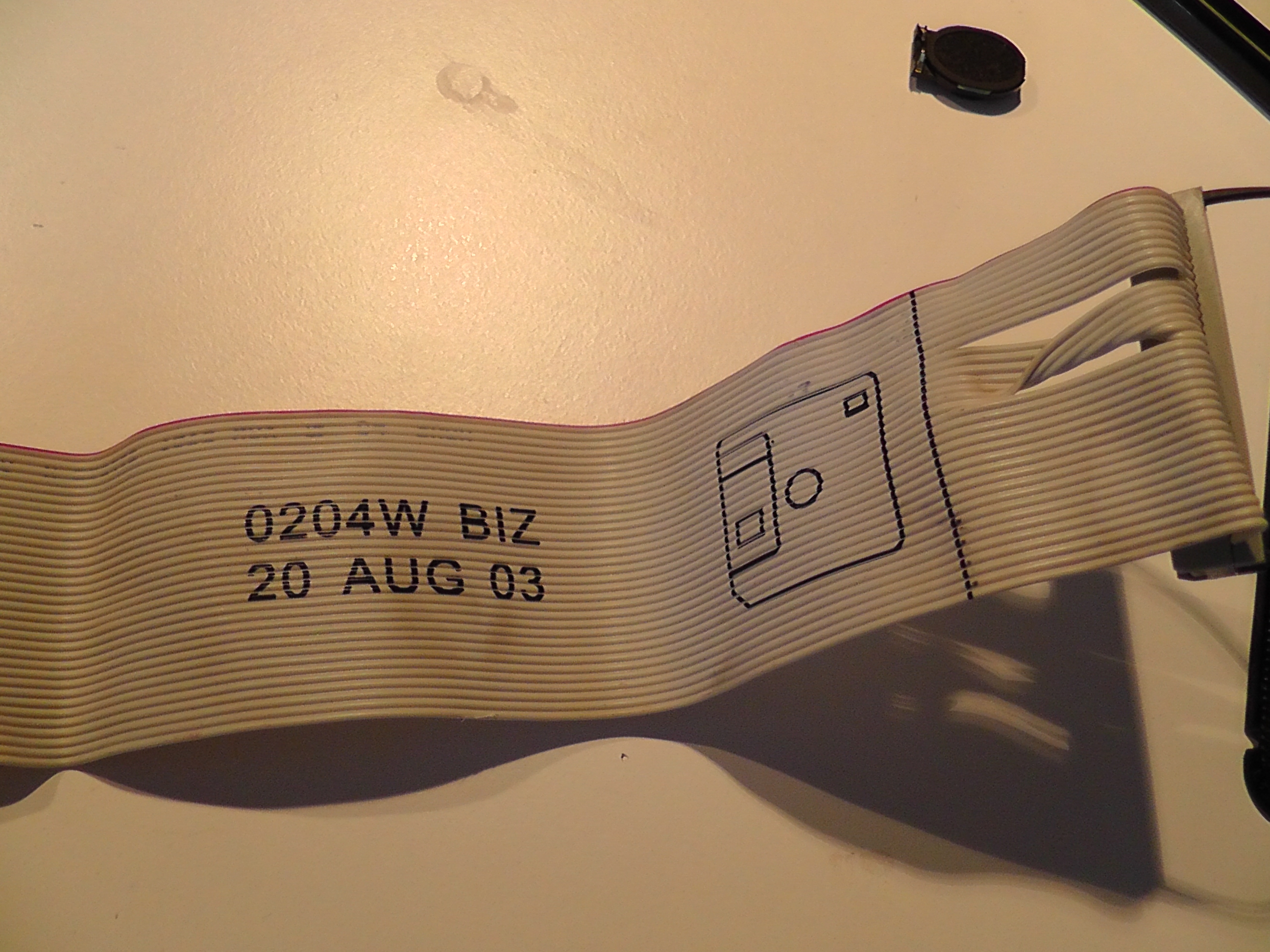
For this project you'll need:
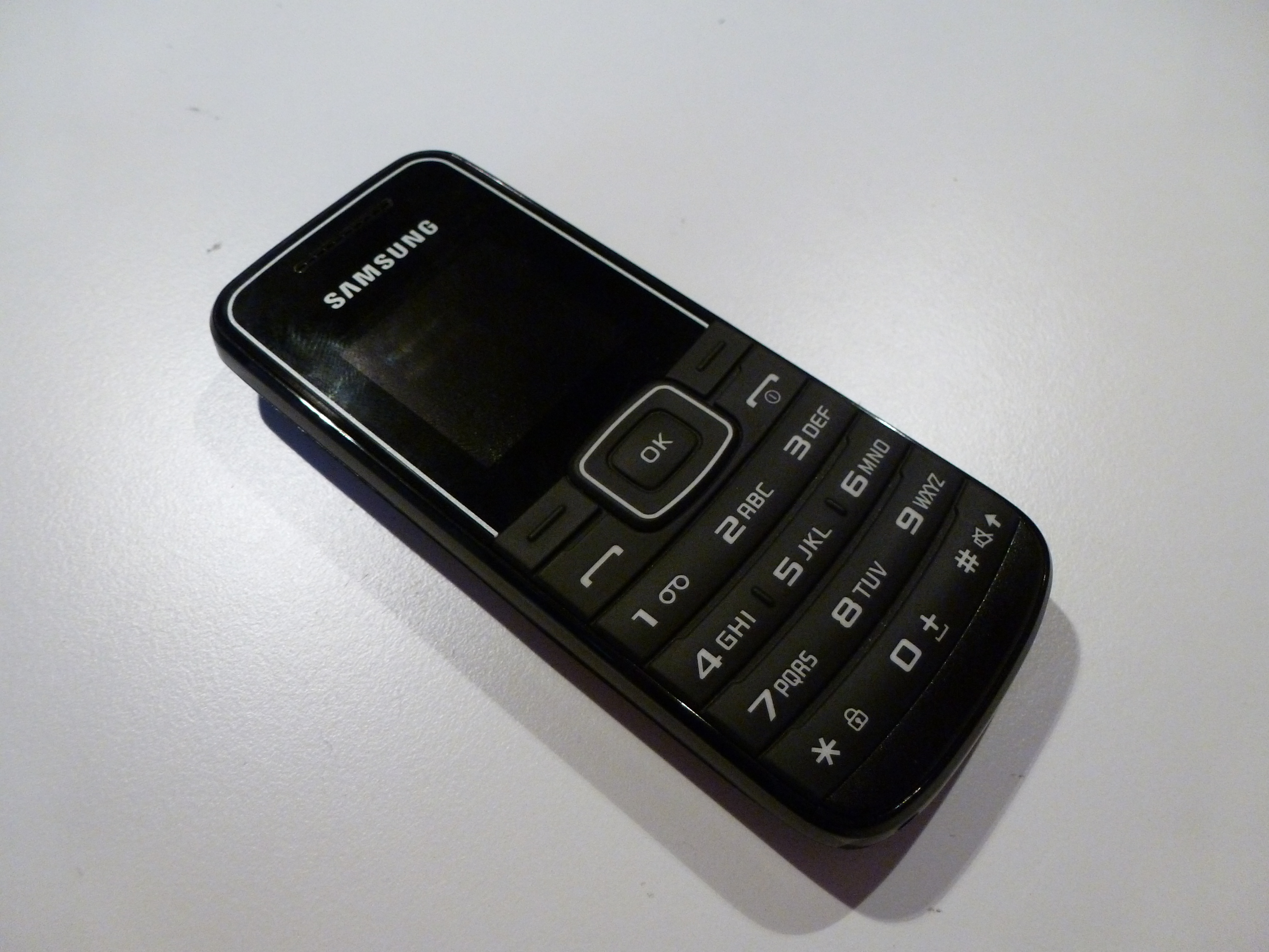
- An old cellphone with keys
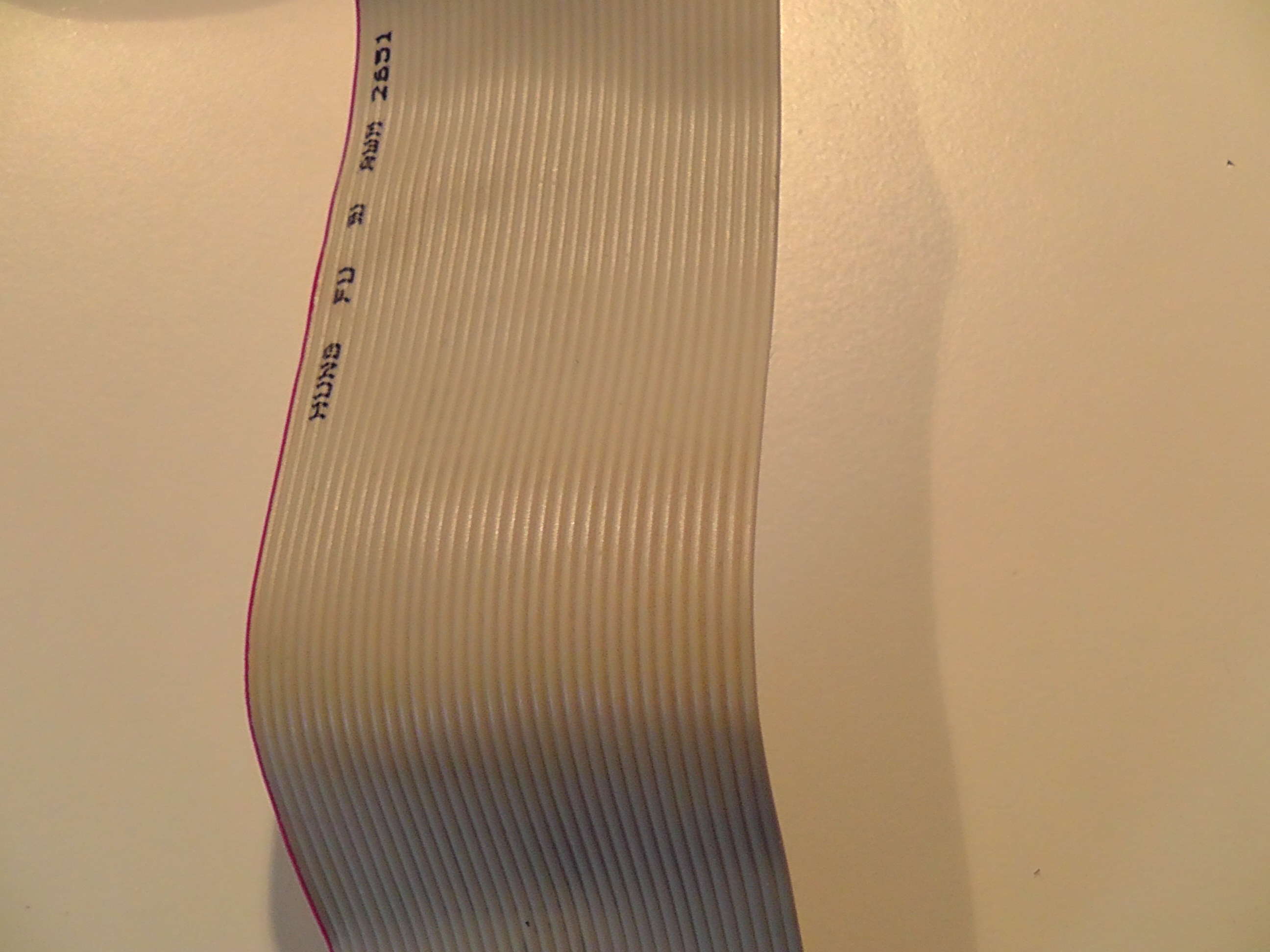
- A ribbon cable from a computer, should have at least 20 contacts
- Perf board, I recommend the '3 hole pad' version where the holes are connected in groups of 3
- As many 2n3904 or BC547 transistors as keys you want to access (21 in my case)
- The same number of 10k ohm resistors as transistors
- 74HC595 shift register ICs
- Some passive components, e.g. filtering capacitors
Tools:
- Soldering equipment
- Multimeter
Open Your Cellphone
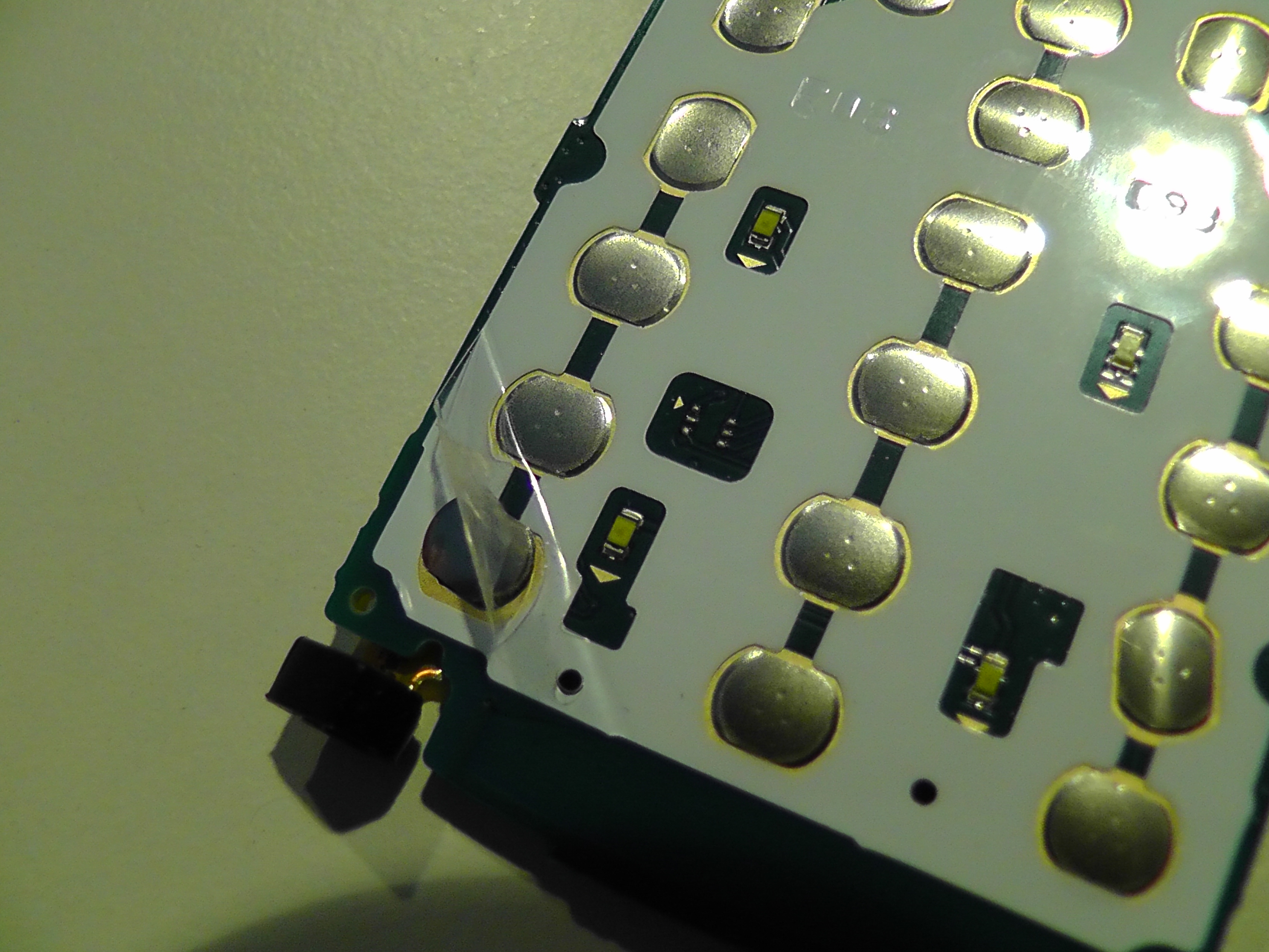
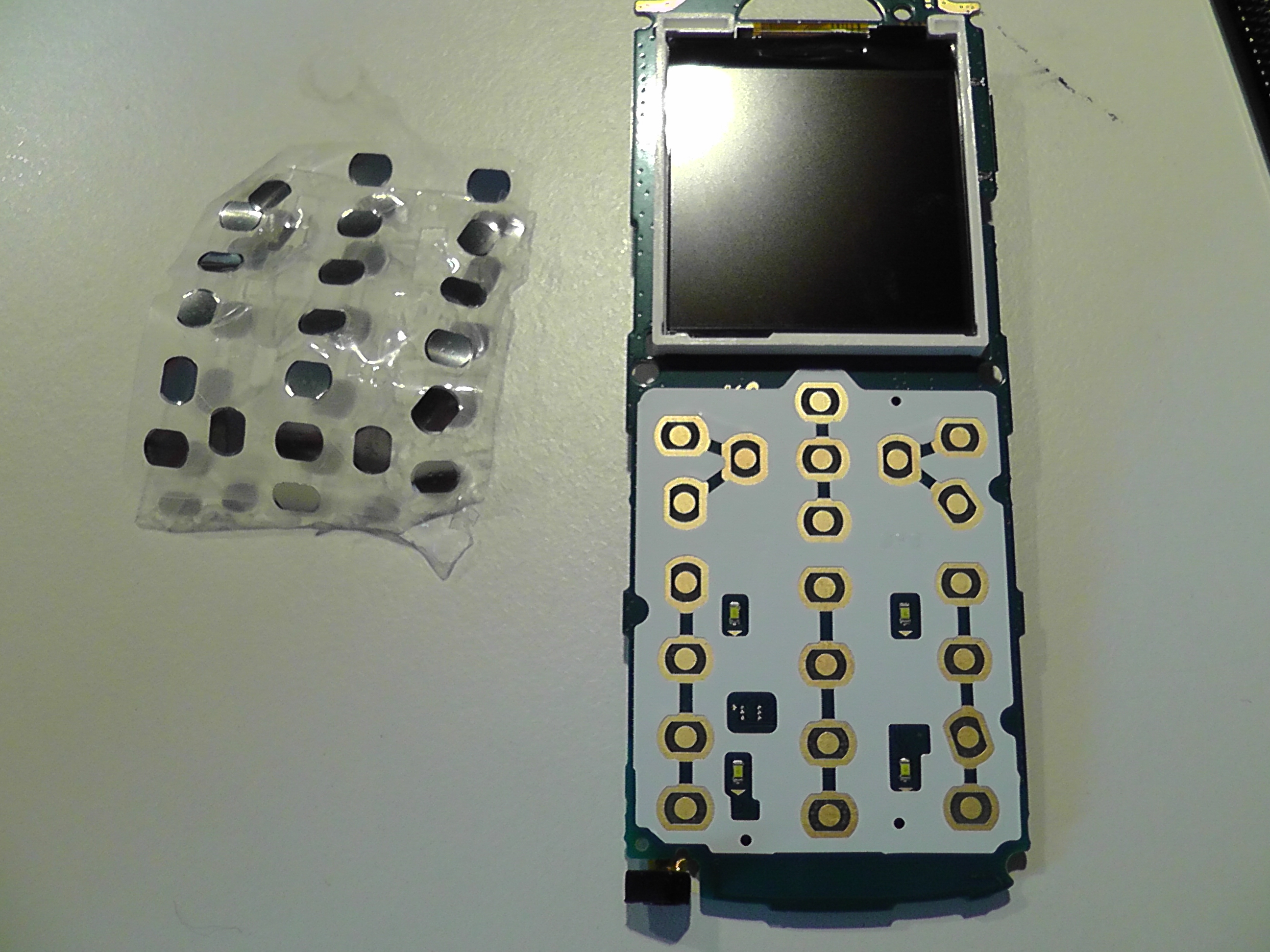
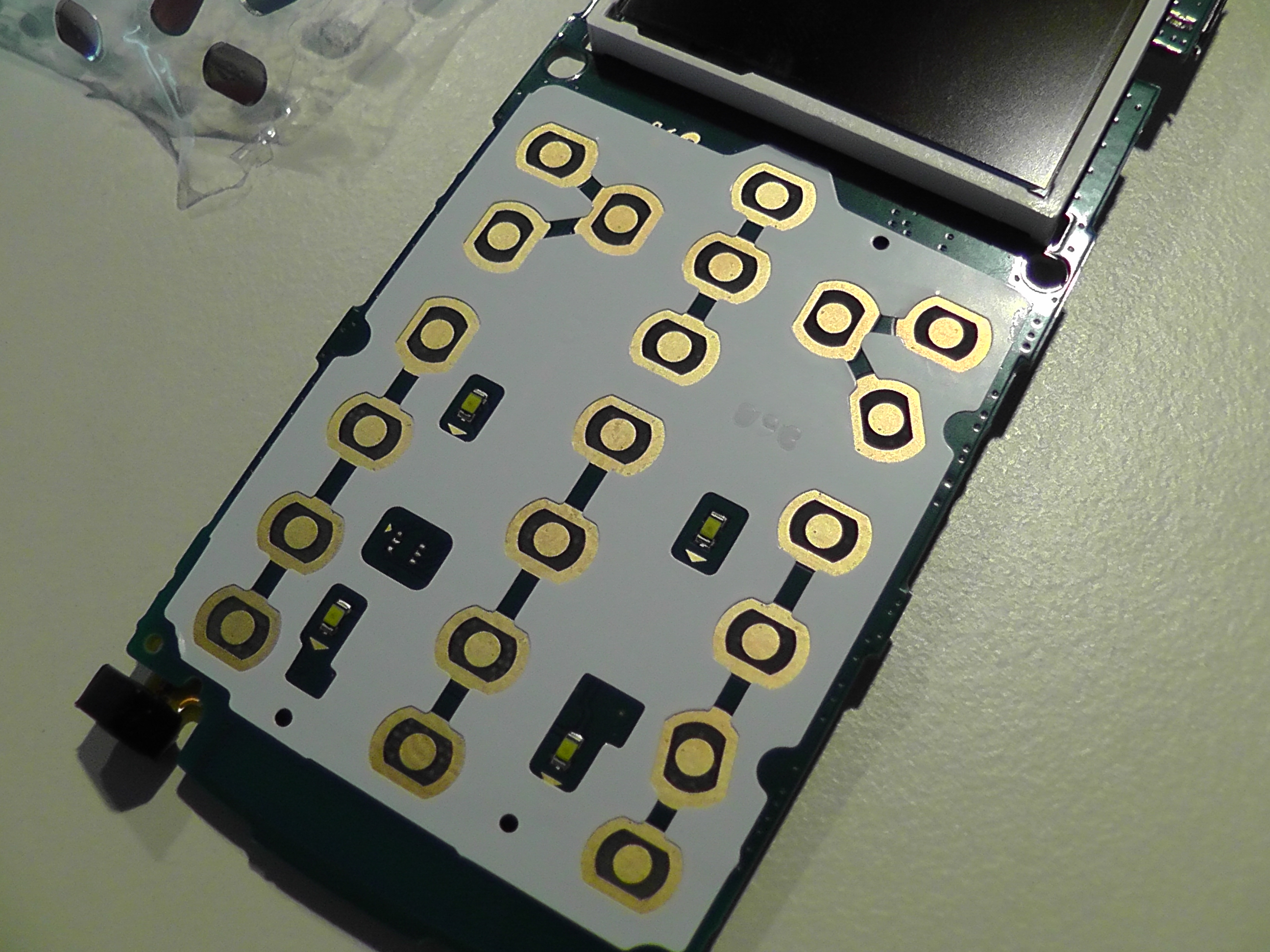
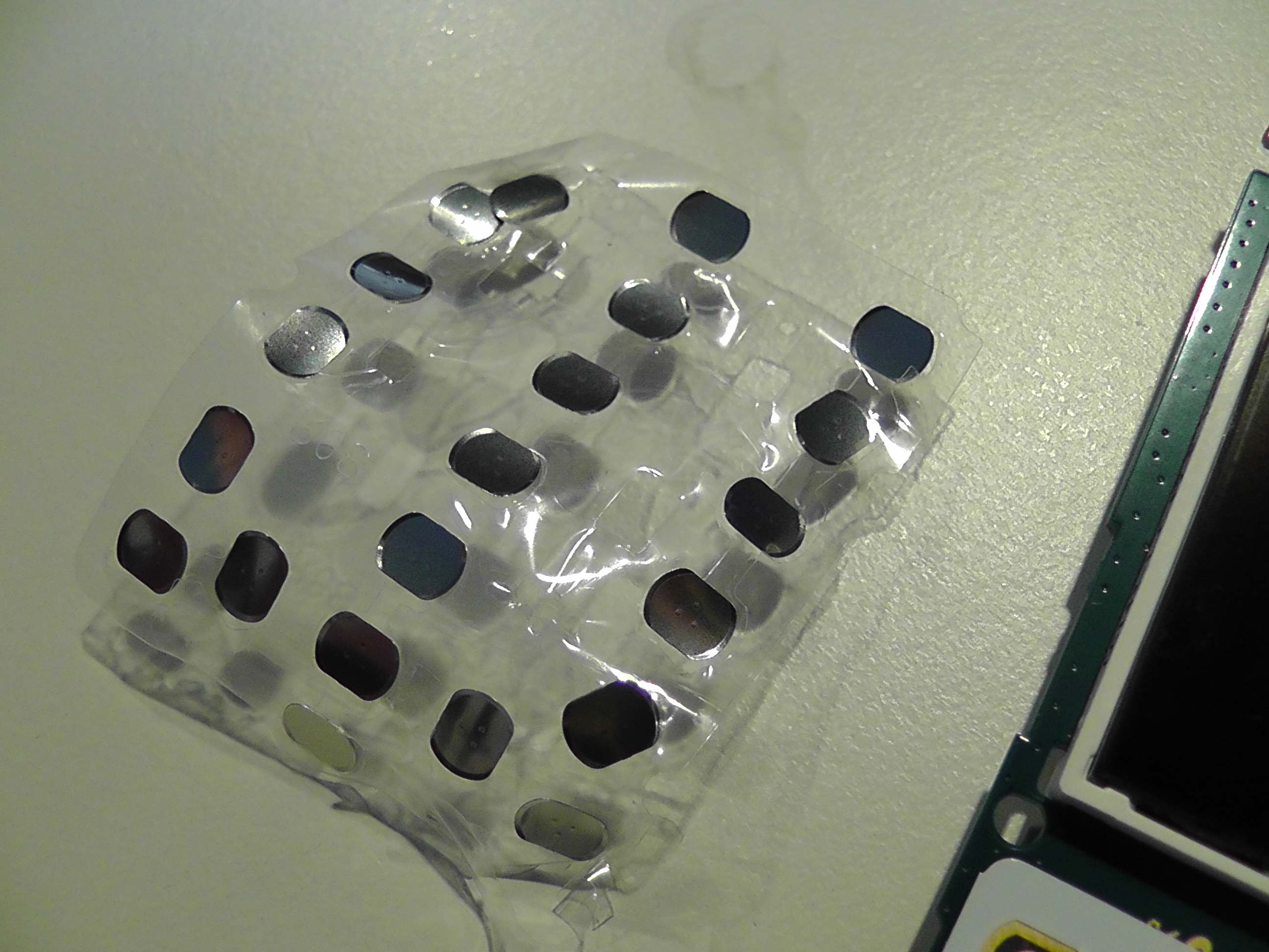
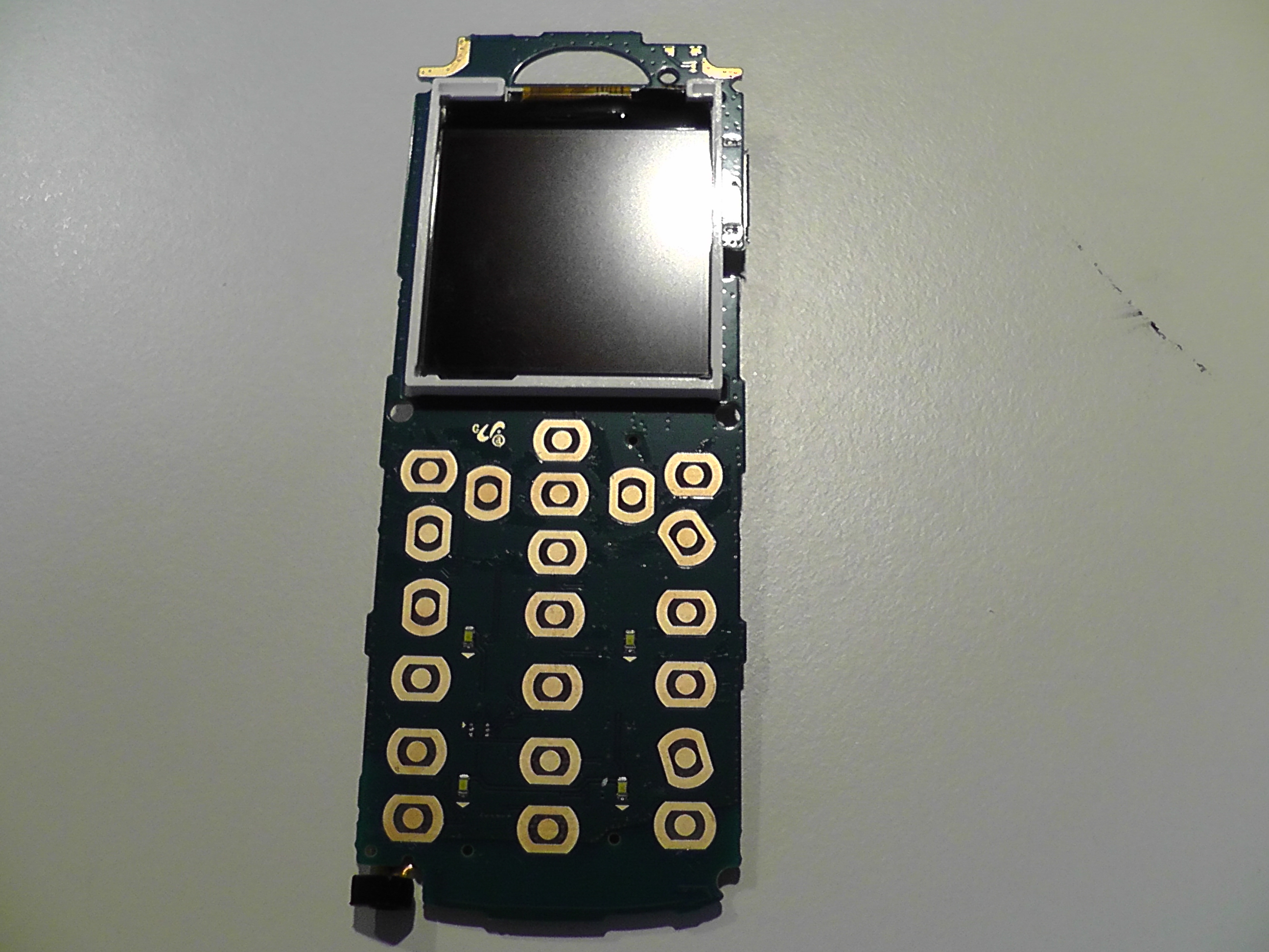
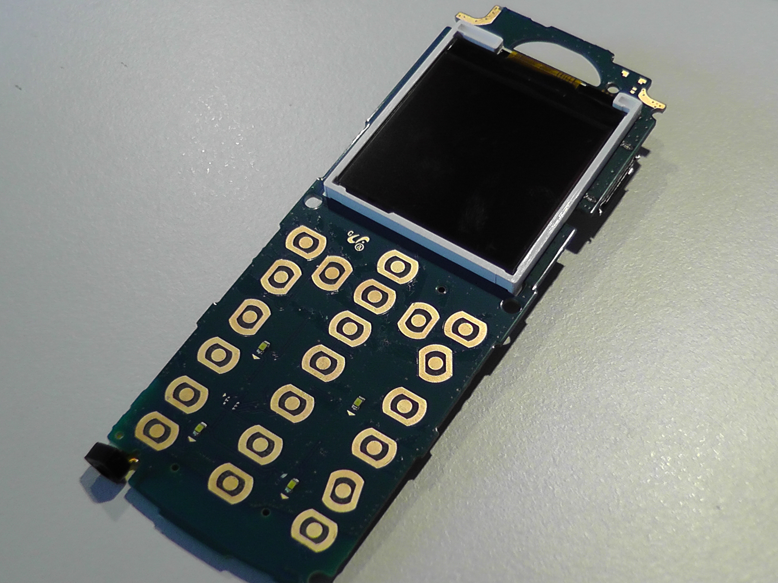
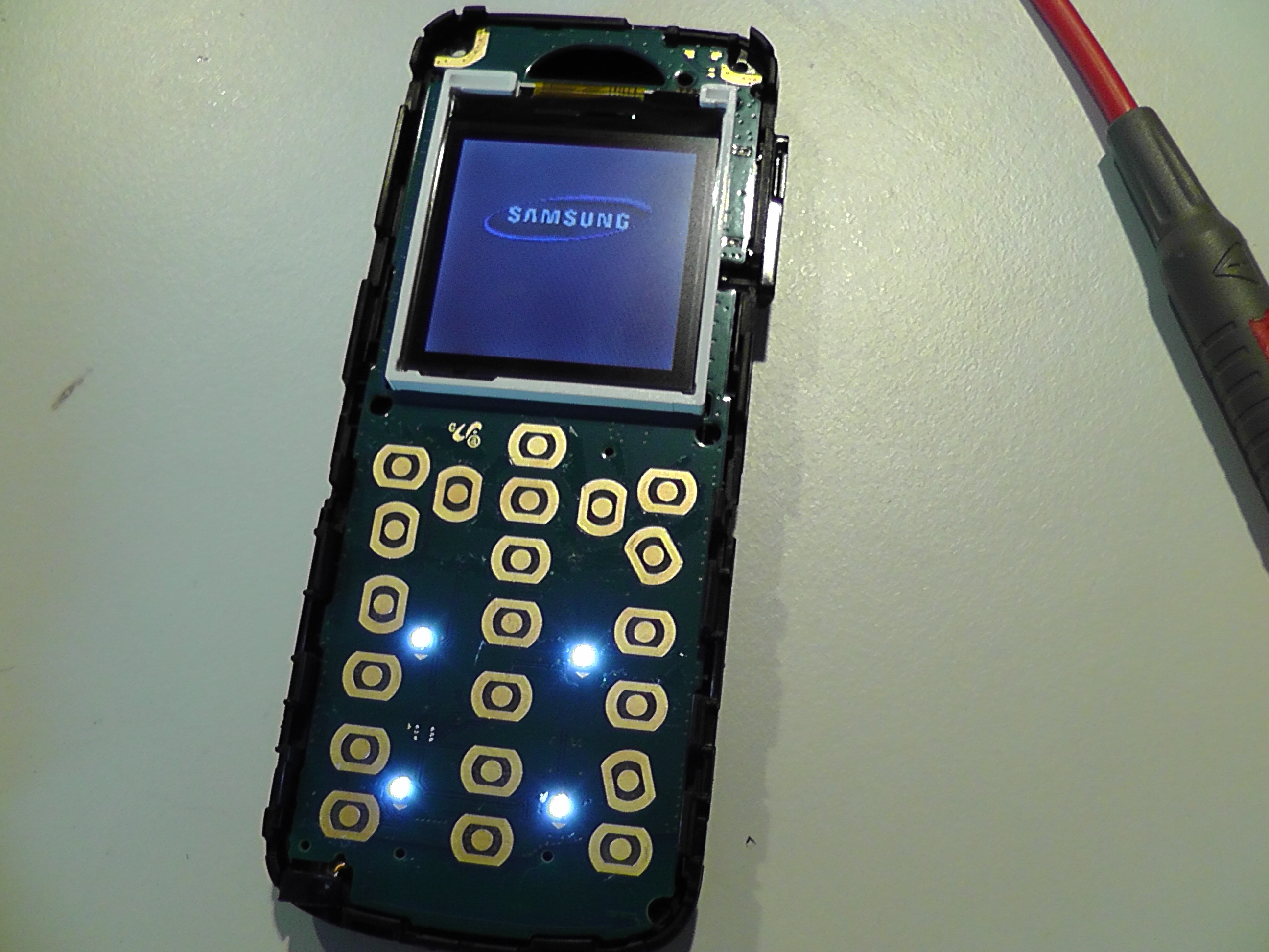
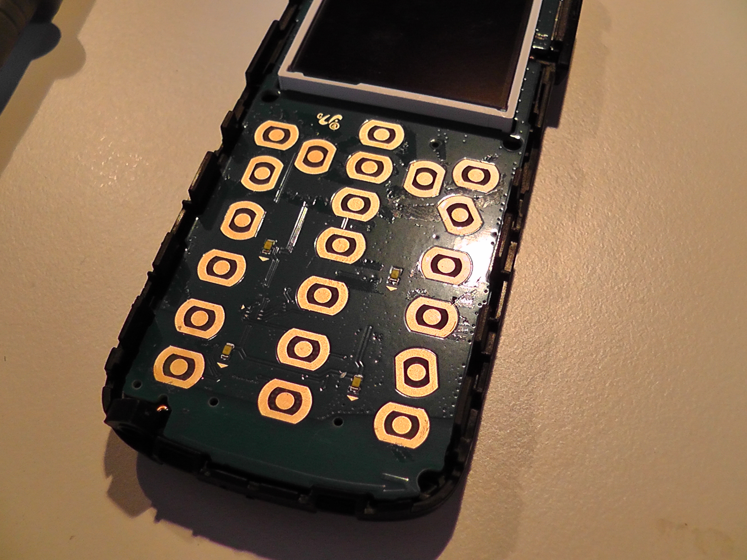
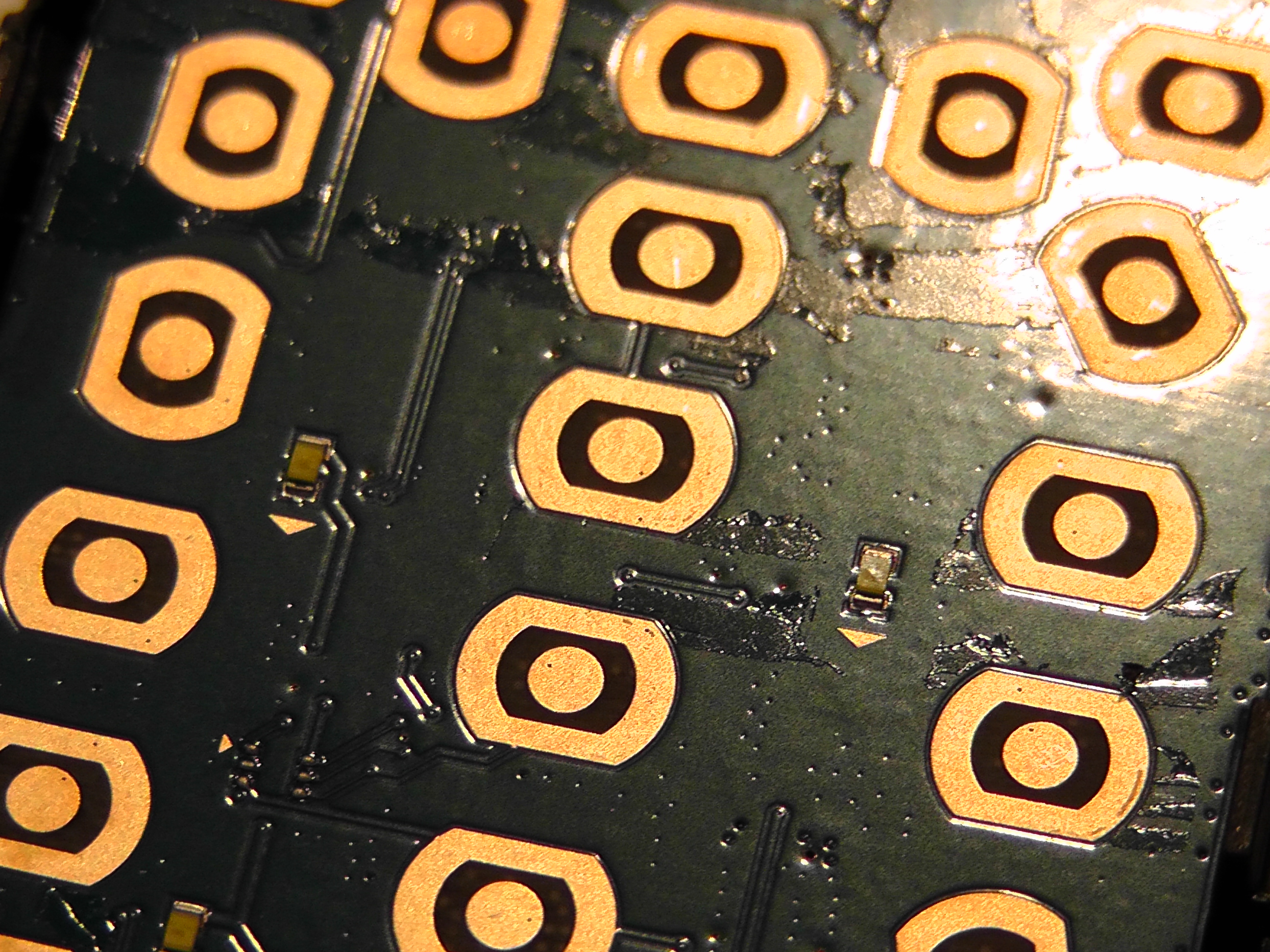
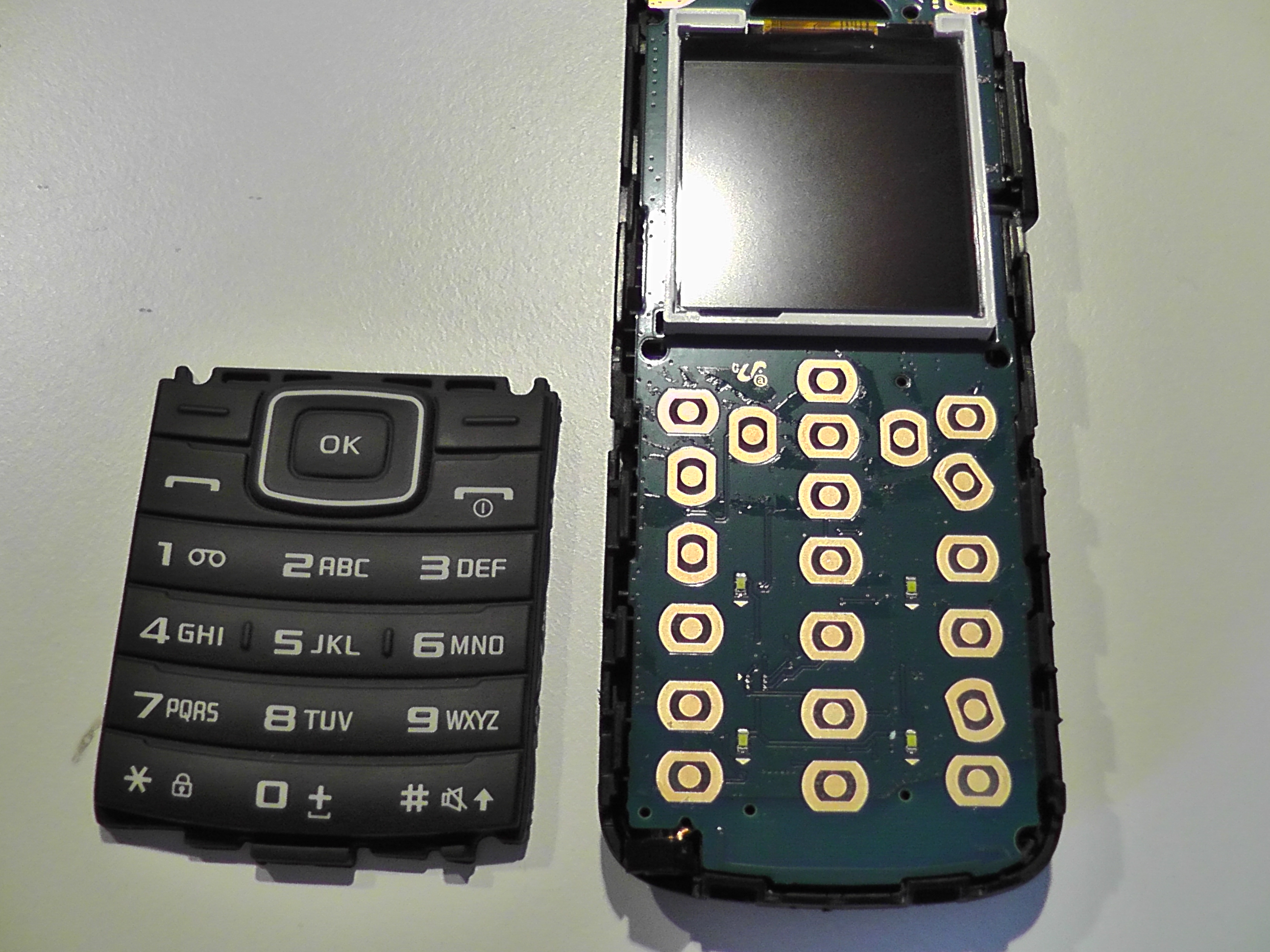
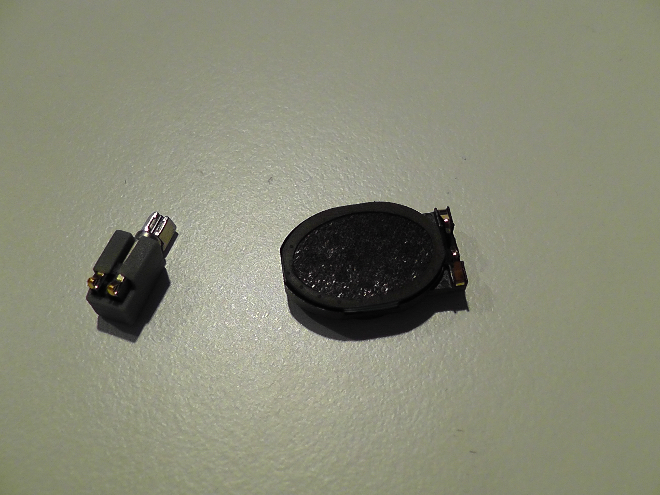
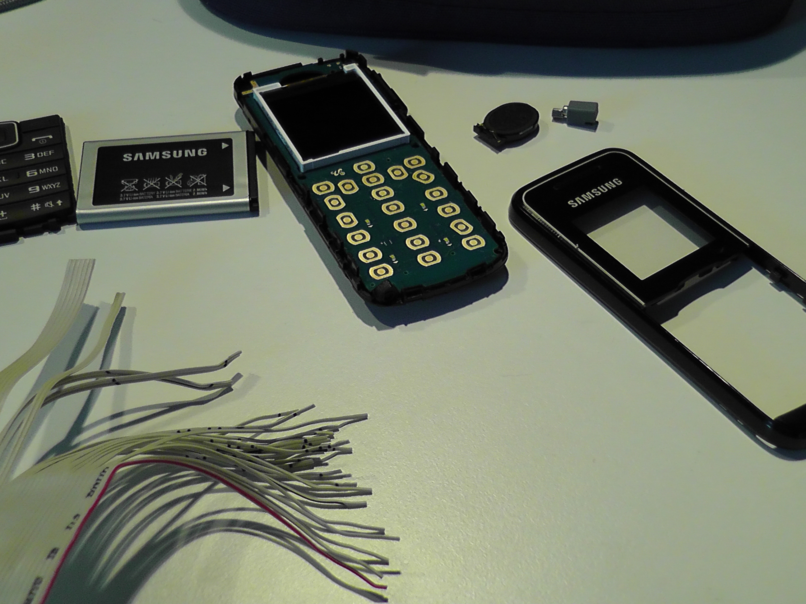
The first thing to do is to open the cellphone until you reach the bare copper pads of the keys.
The pictures included in this step document my journey to the center of the phone. In my case there was a sticker with concave metal platelets on them. These close the connection between the copper contacts and make a clicking sound while doing so.
After exposing the bare PCB with the keys' copper circles I used a scissors to close the connections on the 'on' button, thereby turning the phone on (see the picture with the lit up screen). Do this as well, so you can be sure that you didn't accidentally break your phone while opening it.
Also, take out the speaker and the vibration motor. Remember which connections belong to which piece!
Find Stuff Out About Your Keypad
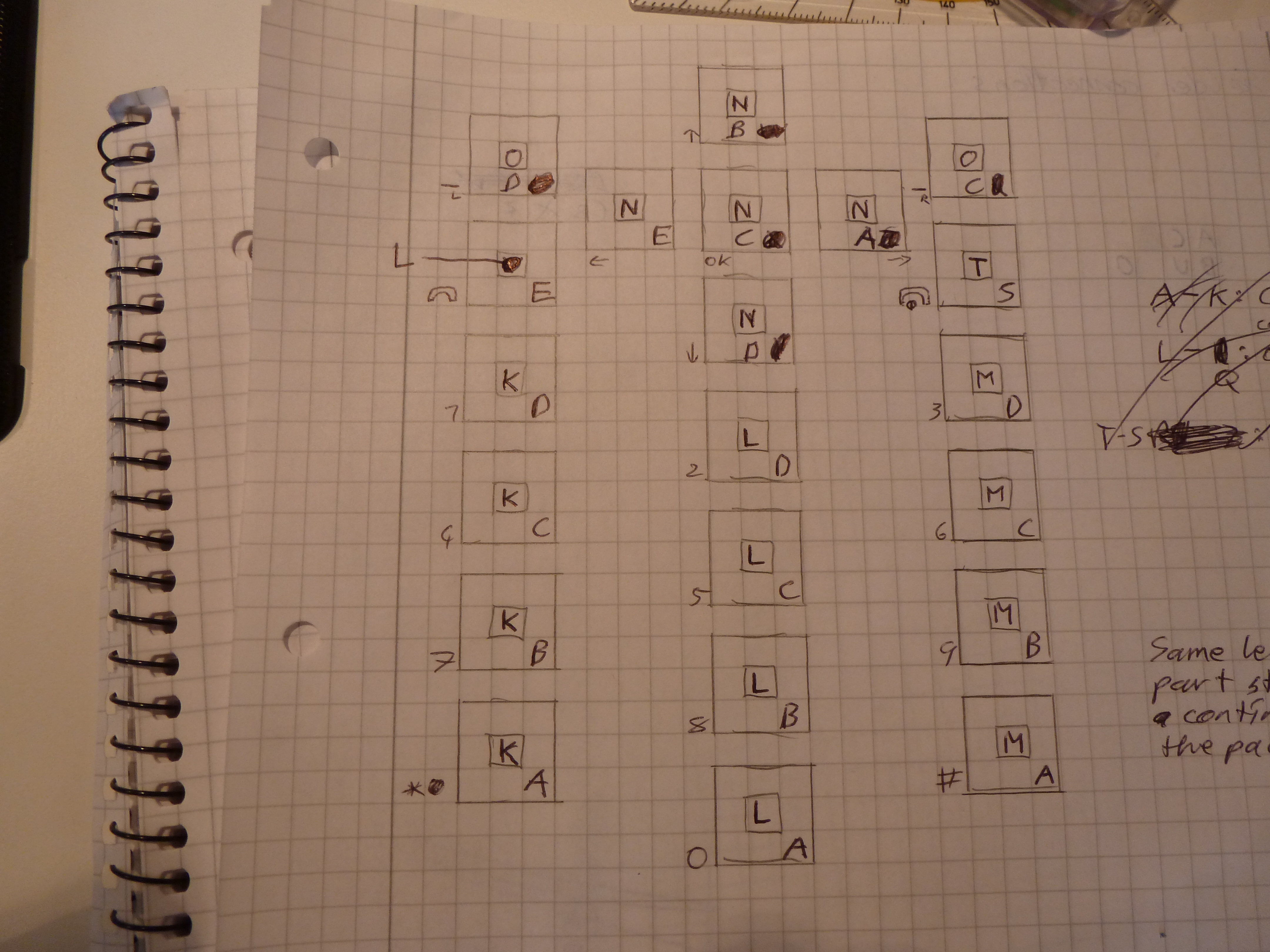
Now where you have the bare keypad, it's time to explore.
Take your multimeter and a notebook and document information about your phone:
- What's the voltage difference between both copper pads of a single button? Which pad is positively charged over the other one?
- Are certain copper pads across the PCB connected with each other? Which ones?
These are the results of my testing:
- The center copper pad of a key is charged by 2.7V more positive than the outer copper pad
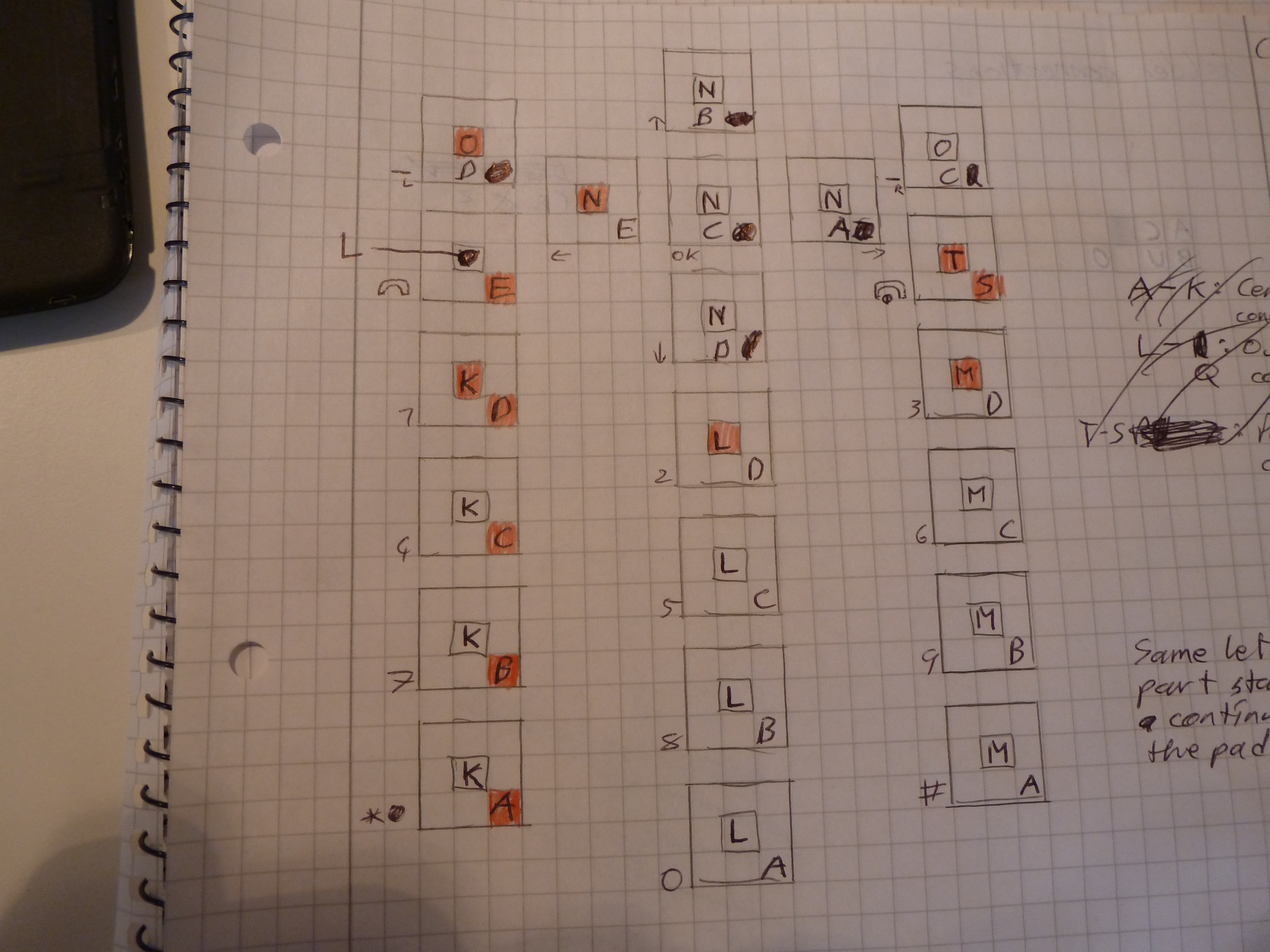
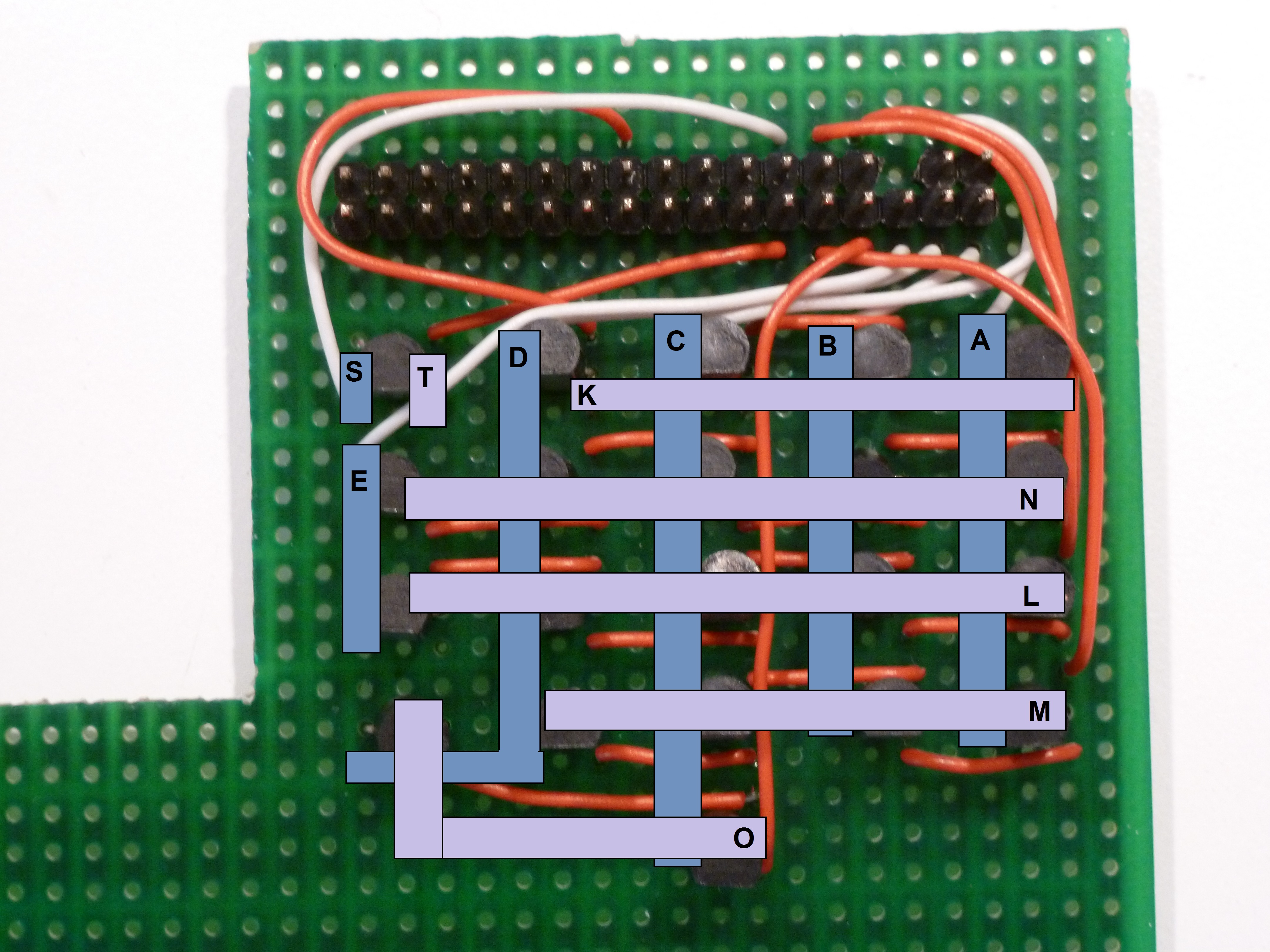
- Many copper pads are connected. As you can see in the picture I visualized where the buttons are and which pads are connected. Same letters are connected. This results in 12 individual connections for 21 buttons.
- When the phone is off, the 'on' button is the only one that has a voltage across it.
Why do we do this?
This data is important for the external circuitry. The voltage over each key is important for when we want to attach a transistor to the copper pads; polarity matters.
Knowing which pads are connected to each other has more of a practical effect. Later we will need to solder wires to the keys. Of course we could solder a wire to each copper pad, but this would result in 42 (!) single wires (in my case).
By knowing which pads are connected to each other we can solder one wire to one pad from a group of connected pads instead of a wire to each one. In my case this means 12 wires instead of 42! In the picture with the red-highlighted letters, you can see which pads wires will be soldered to. It saves you lots of work!
Soldering
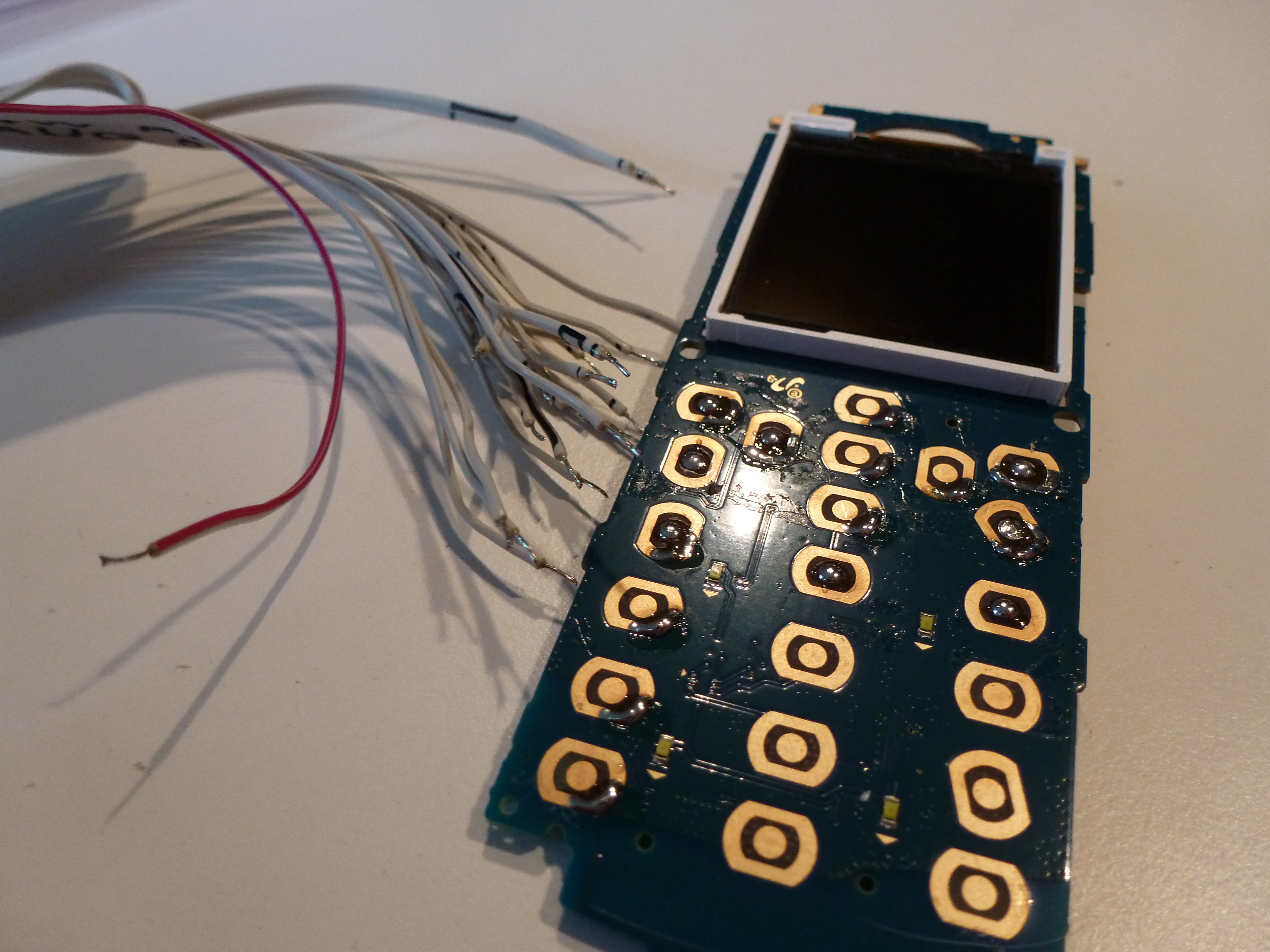
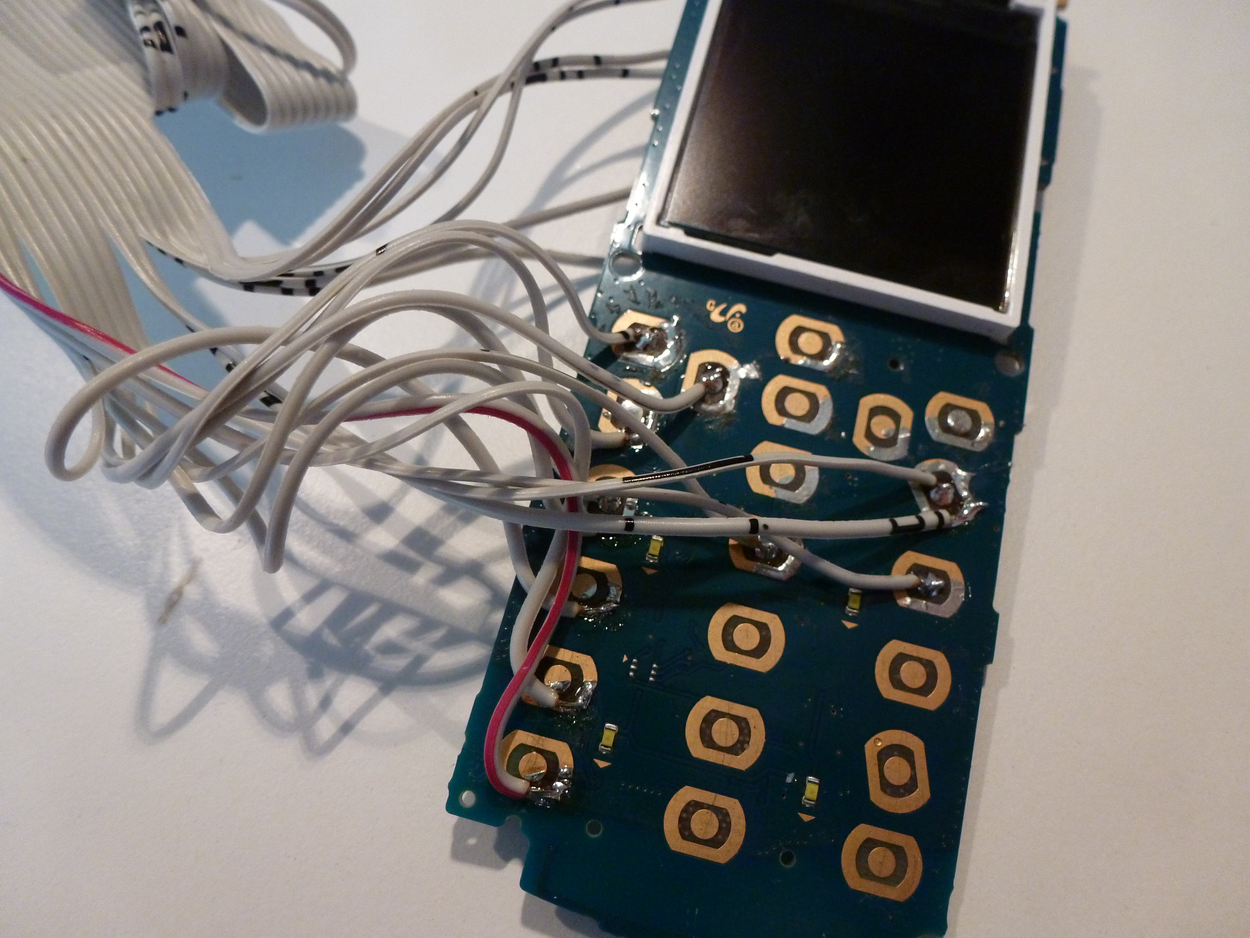
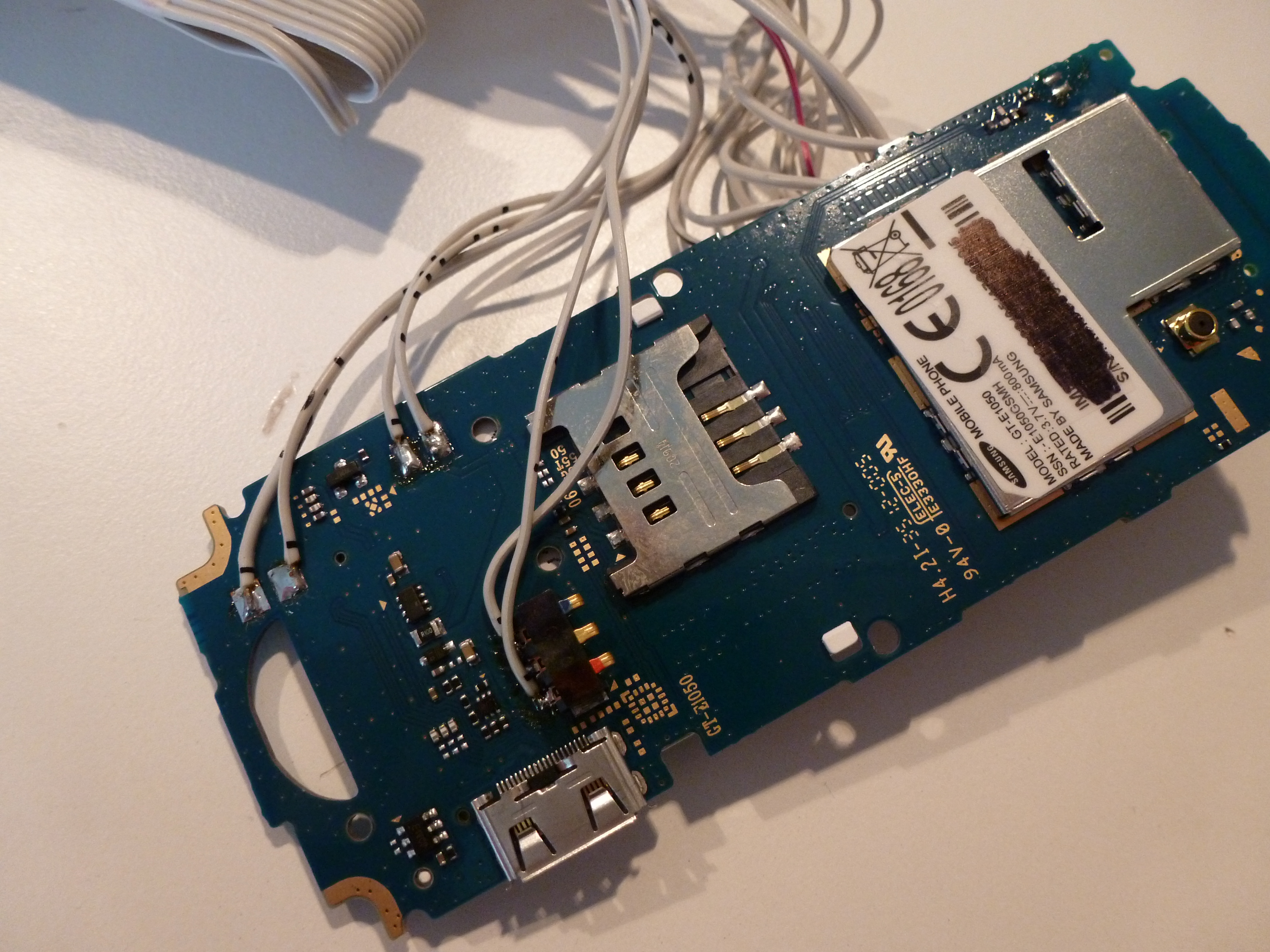
Now take your ribbon cable and select a wire for every pad you must solder and for each connection of the vibration motor and speaker. Also you will need to solder wires to the battery connector of the phone.
Peel the required wires apart, strip them from their insulation and tin them. Make sure to only strip about a millimeter or two (=~1/12 inch) of insulation, you don't need more.
Now solder the wires. Make sure not to short out any connections and make sure the phone is off and the battery removed.
Testing the Connections



Now that we have soldered, we must now test.
Take your multimeter, set it to test continuity (the mode where the meter beeps if the bare test leads are touched).
- Stick a bare piece of wire into each pin on the female side of the ribbon cable.
- Touch this wire with one multimeter test lead.
- Take the other lead and touch the pads the wires are soldered to.
- If the meter beeps, write down which pin is connected to which pad (like in the pictures included).
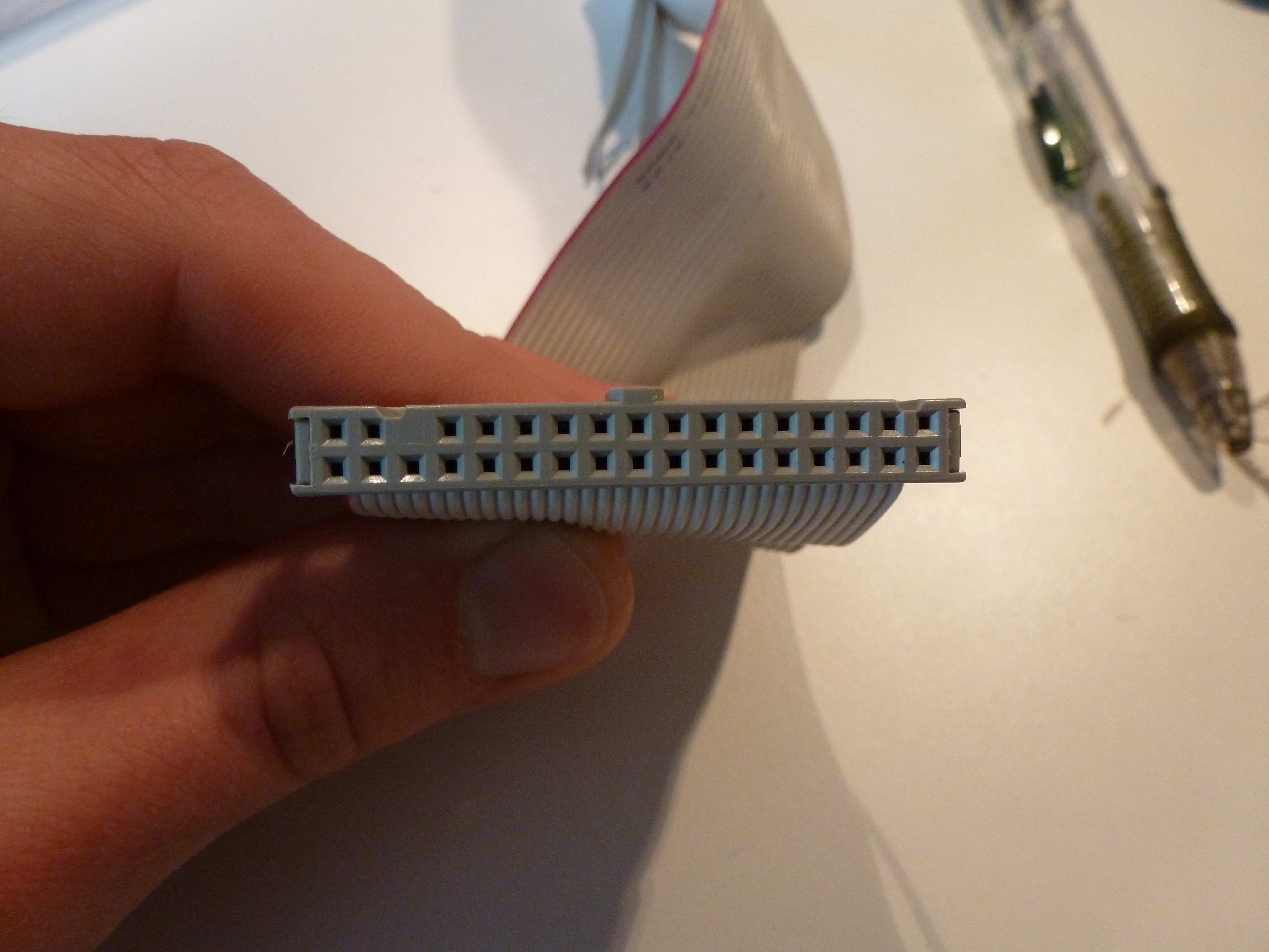
If you end up with a pad that has been soldered to but doesn't connect with any female pin on the ribbon cable, you have the same problem I had. Count the number of wires on the ribbon cable. Count the number of female pins. Are these two numbers the same? Mine weren't. That's because there is a wire on the ribbon cable that should connect to the pin that is now solid plastic (see the picture of the female connector).
If this is what happened to you, simply desolder the wire to the pad that isn't connected and use a different wire from the ribbon cable.
If this story doesn't apply to your case, you've soldered badly and must resolder the connection.
Double check that you haven't bridged any pads!
Soldering Part 1: the Transistors
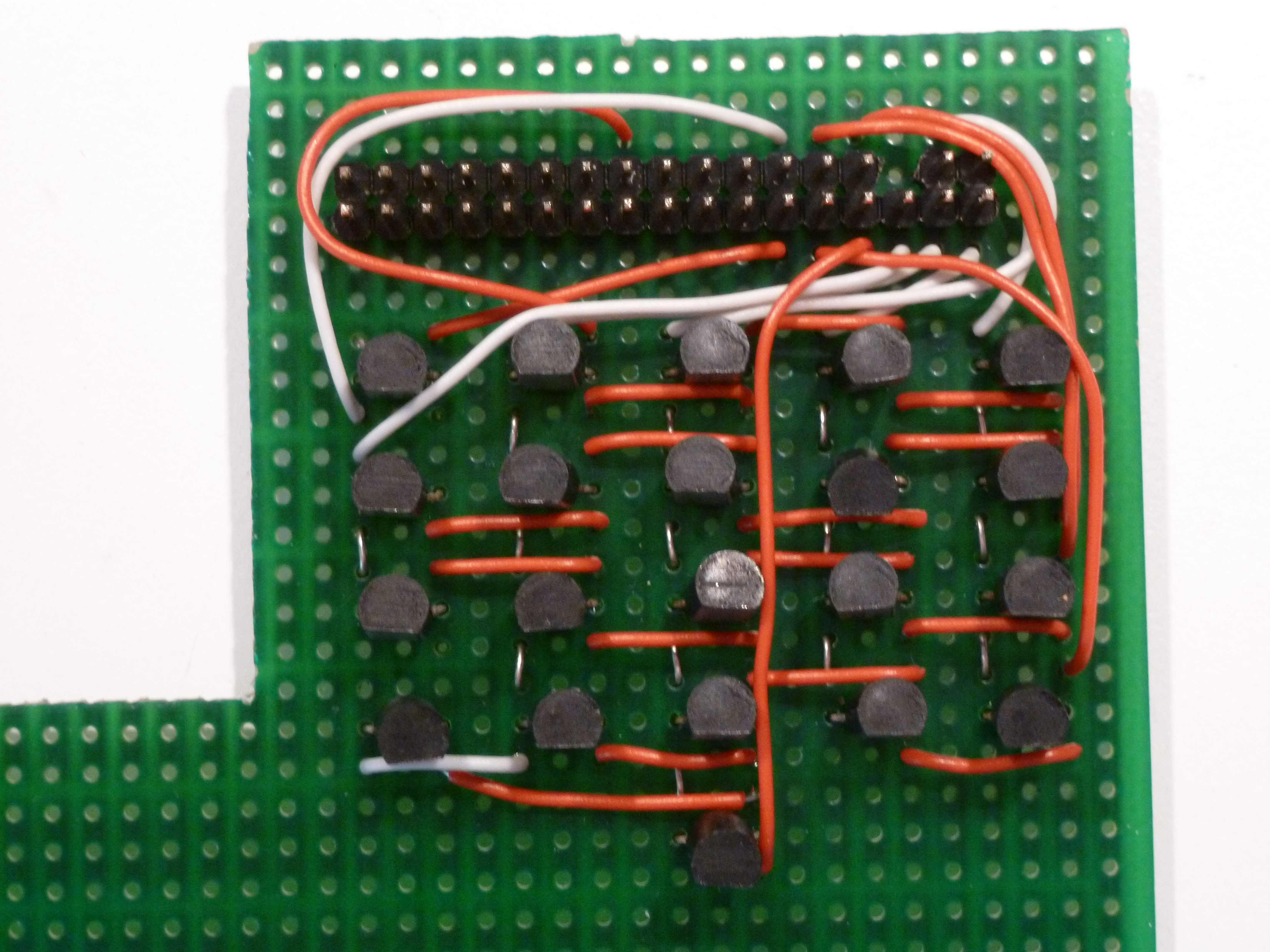
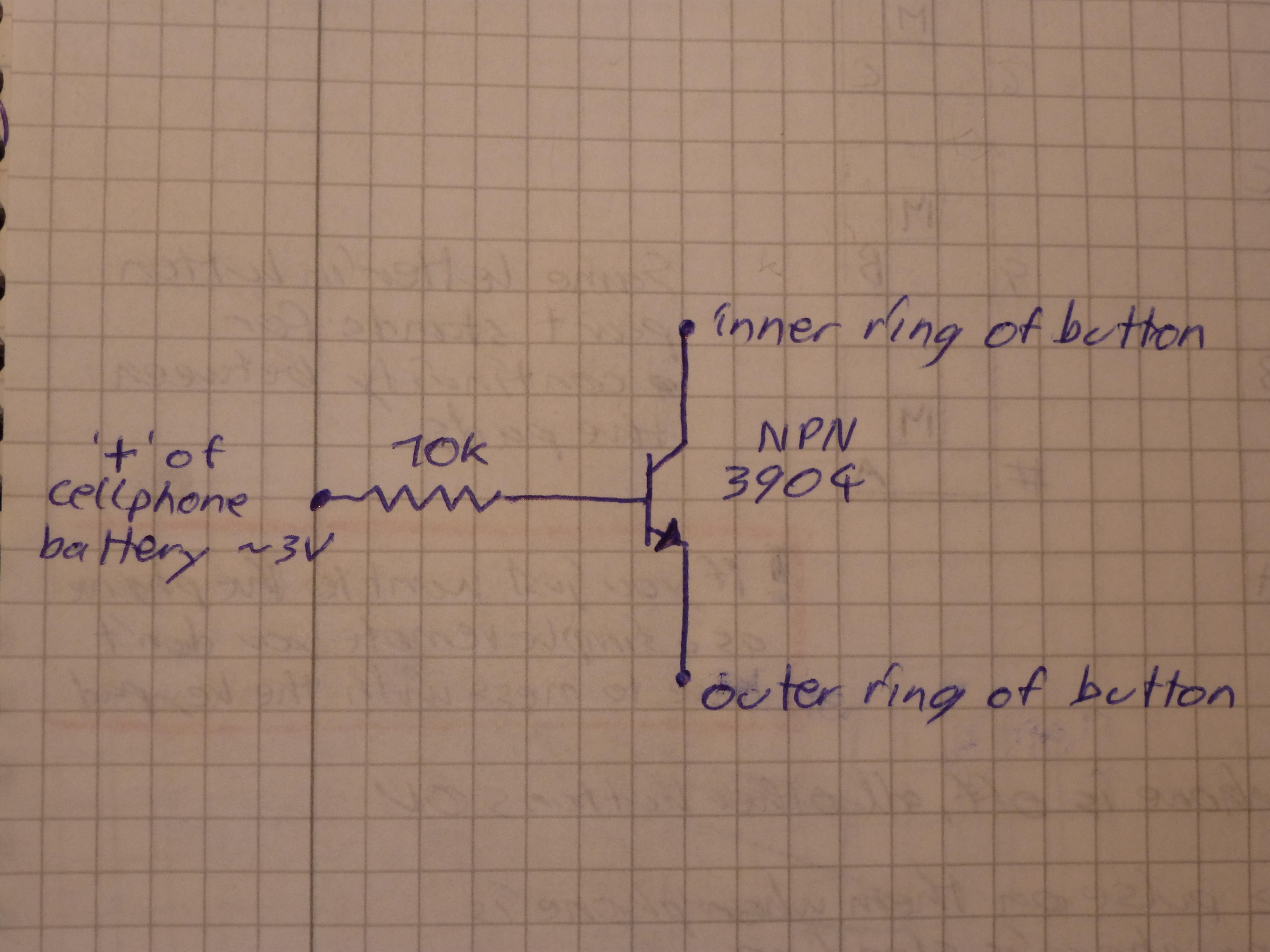
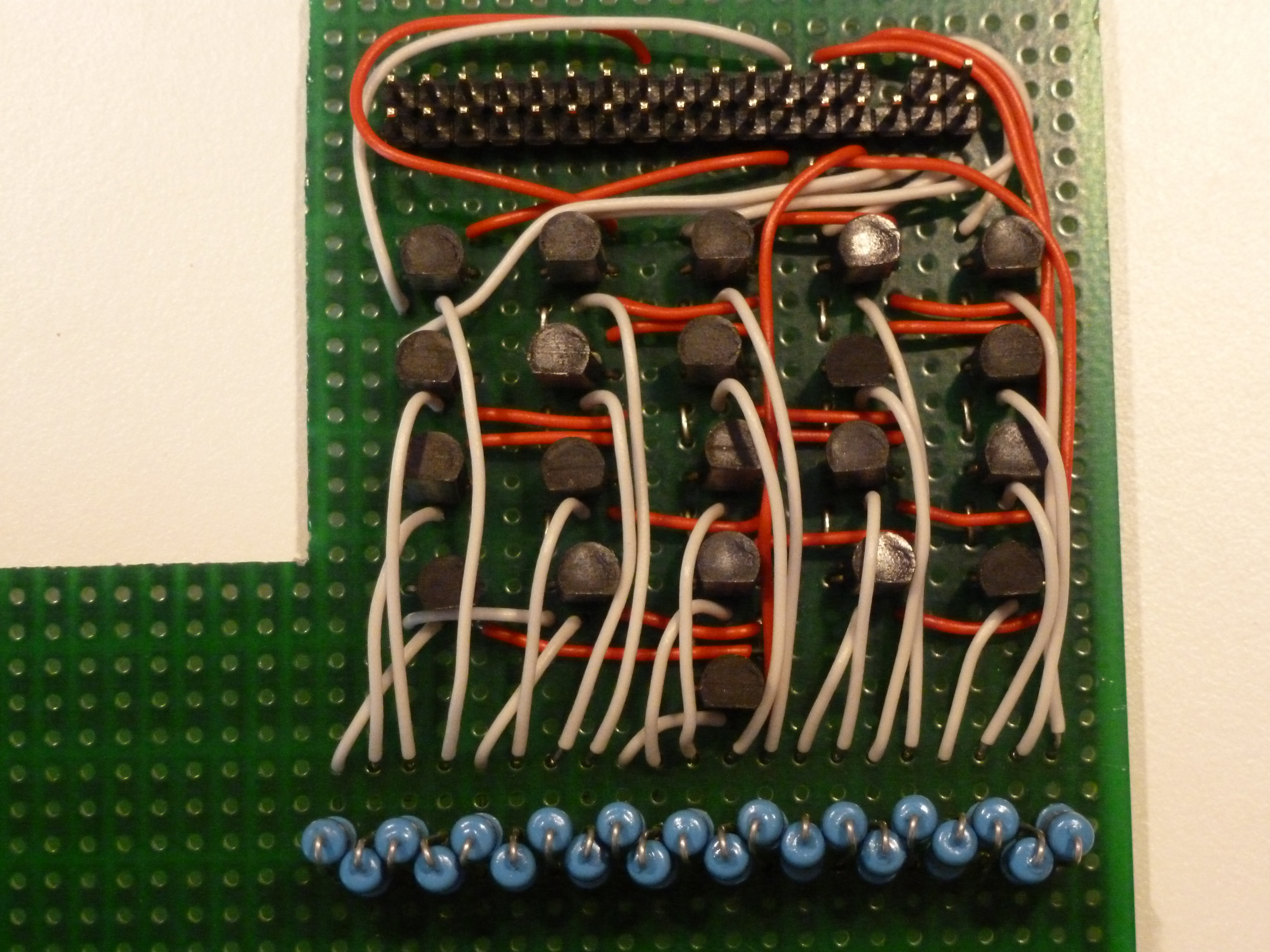
Now we must solder our components onto our perf board, starting with the transistors.
The connections from the positively charged copper pads must go to the Collectors, the other connections connect to the Emitters. In my case the K,L,N,O,M and T pads were the positively charged ones and the A,B,C,D,E and S pads the others. My center pads were always charged by 2.7V more positive than the outer pads. Picture 3 shows the resulting schematic for each transistor.
As you know we "compressed" the connections from the 42 copper pads to 12 wires, based on their continuity. Now we must "decompress" these 12 wires back to 42 connections which go to the transistors. This means a wire must connect to several Collectors/Emitters.
Due to this I recommend aligning the transistors in a grid and connecting the collectors of all transistors in a horizontal line and the emitters in a vertical line (see first two pictures).
You must find the right solution for your situation.
Solder in some pinheads to attach the ribbon cable to and connect the emitters and collectors of the transistors to them.
After that we must solder each of the bases of the transistors to the 10k resistors. I personally didn't have room to directly solder them to the transistors so I first soldered in some extensions (see fourth picture).
Soldering Part 2: the Shift Registers
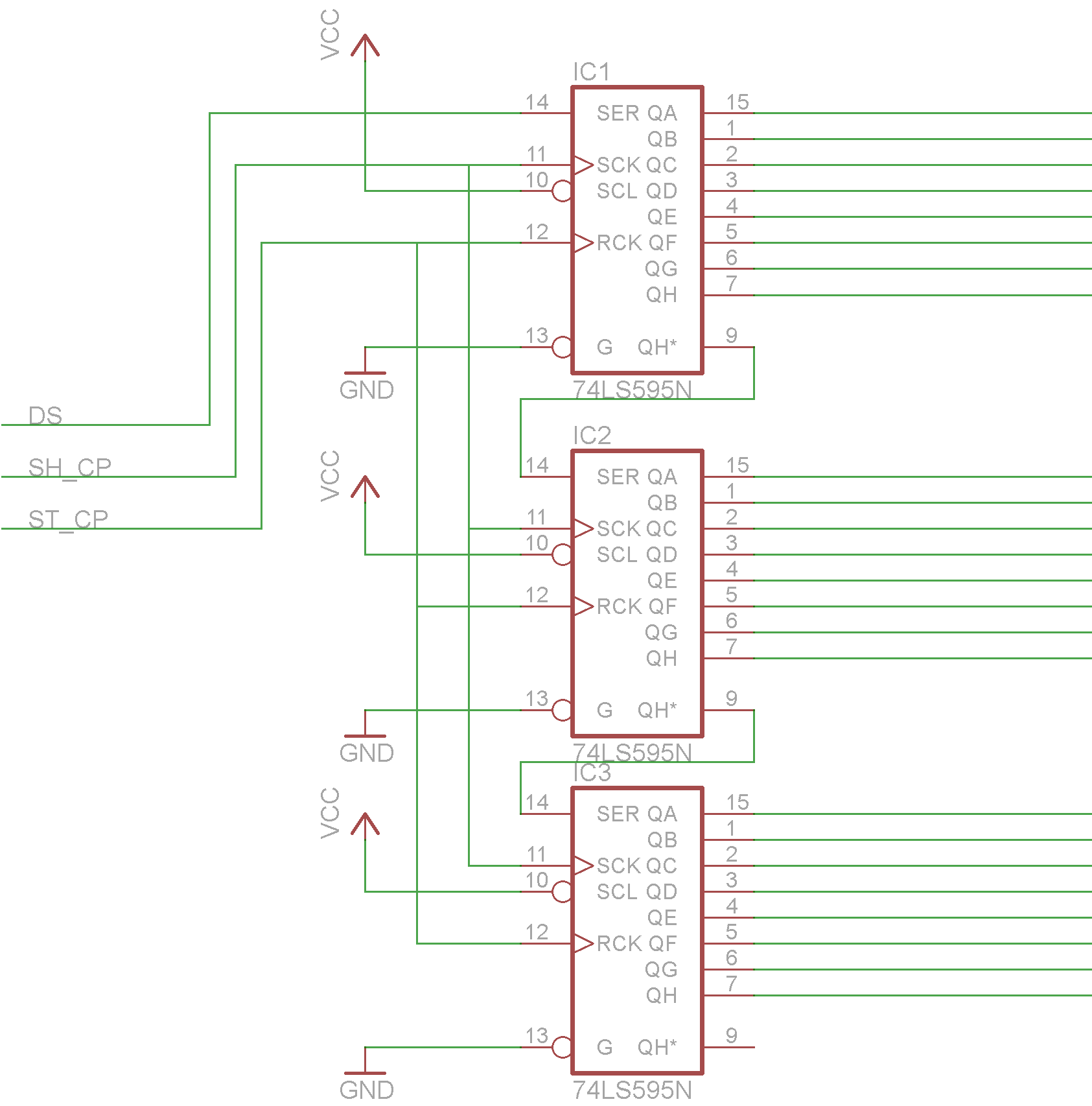
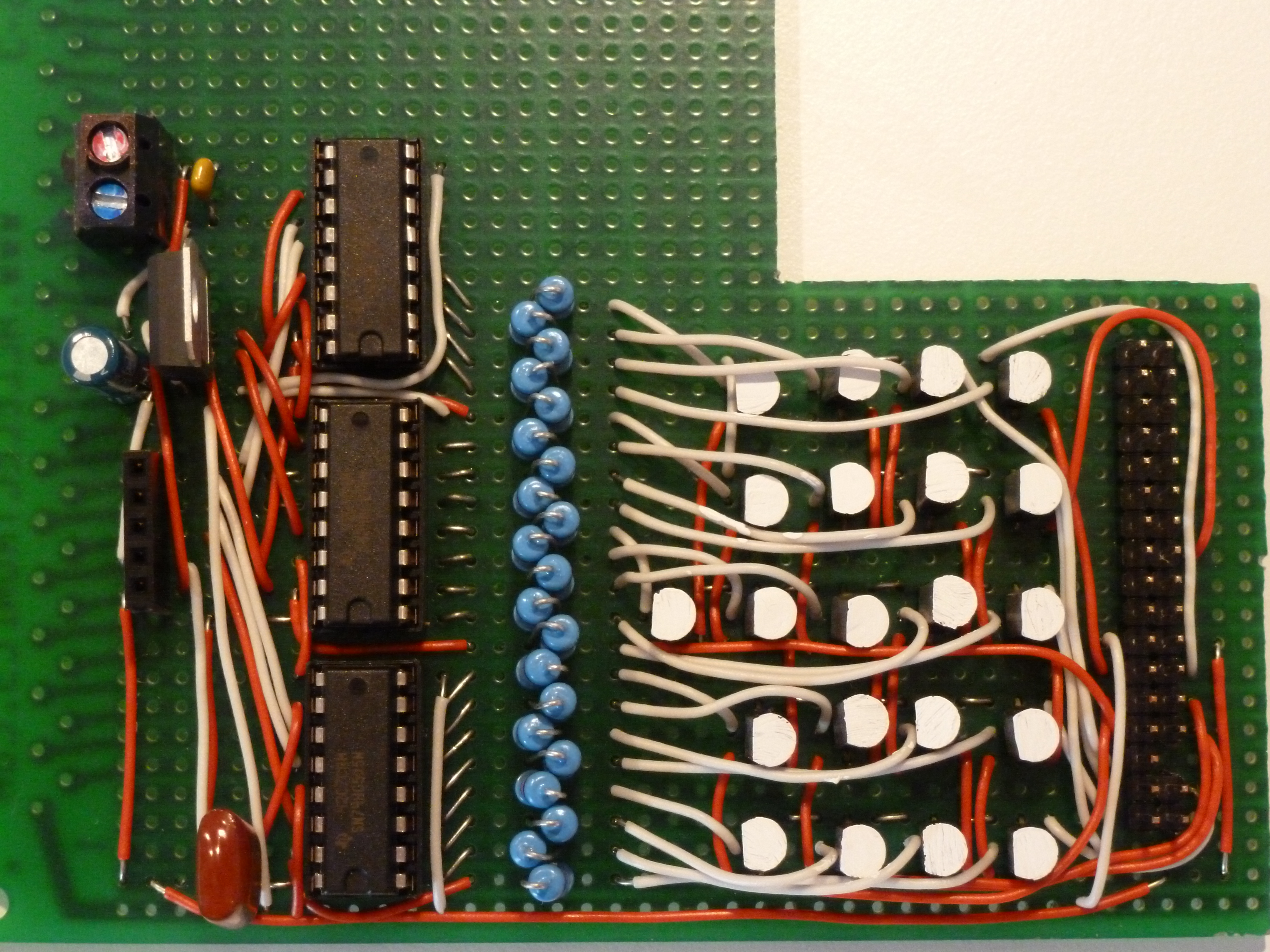
After soldering the transistors we must add shift registers and connect their outputs with the bases of the transistors.
Because I had 21 buttons to press and a shift register has 8 outputs I needed 3 of them to do the job. If you have 16 or less buttons you only need 2 shift registers.
The first picture is the schematic of the circuit we are now going to add. To the left are the inputs that will be later addressed by the arduino. To the right are the outputs that are to be connected directly to the resistors of the transistors. The schematic features 3 74hc595 shift registers with output latches that are in a chain configuration, meaning that the serial output of the first is connected to the data input of the second, and so forth. This way we only need to address one shift register to access the outputs of all others. Because all shift registers need to be in sync, their clock pins need to be connected with each other as well. These are the shift register clock pin (SH_CP) and latch clock pin (ST_CP). The terms SH_CP, ST_CP and DS (for the data input) are derived from this data sheet.
Feel free to solder the shift registers to the perf board as you like, but I recommend facing the side of the outputs to the resistors, if you lined the resistors up like I did (see second picture).
Soldering Part 3: Some Additions
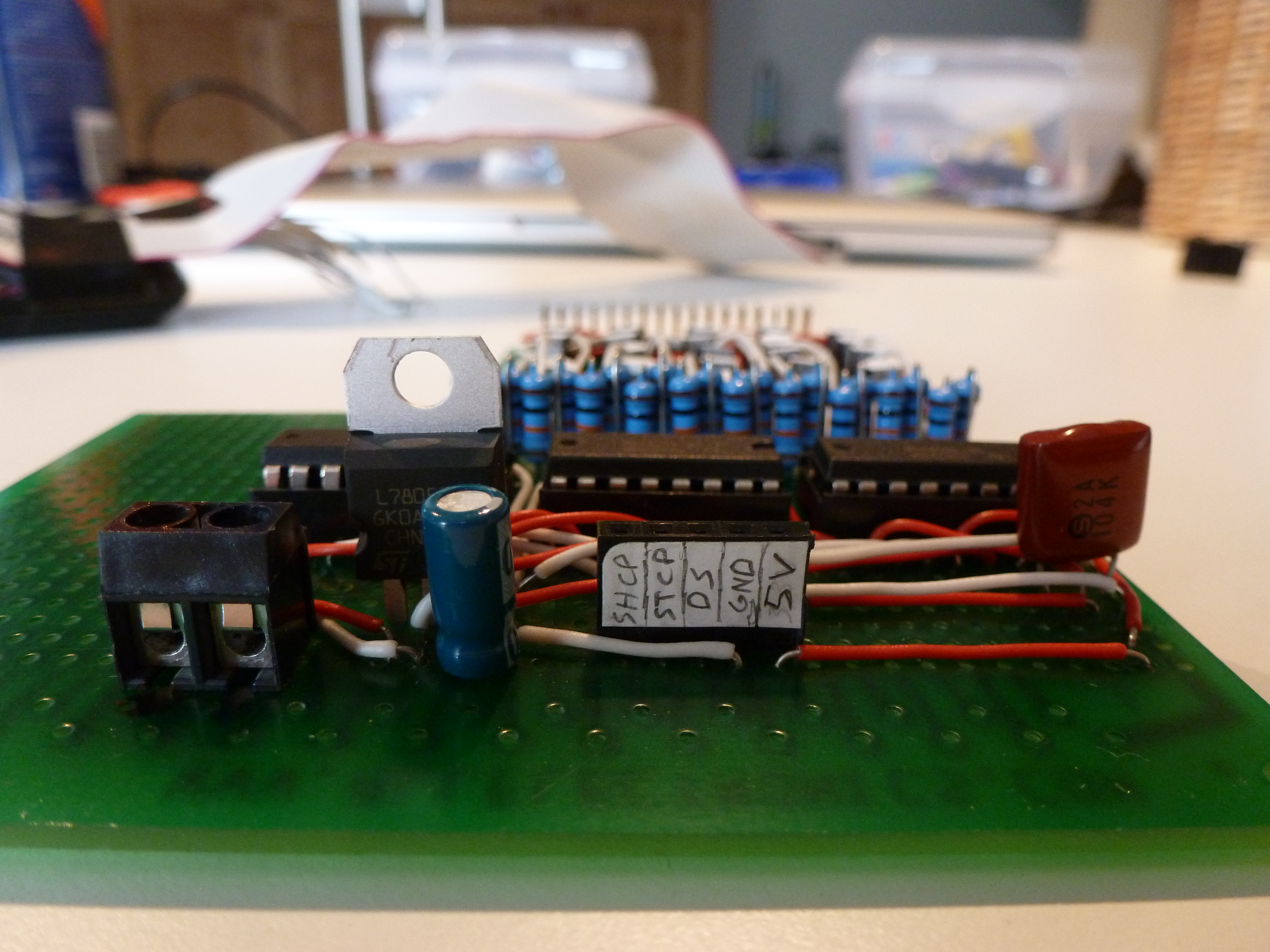
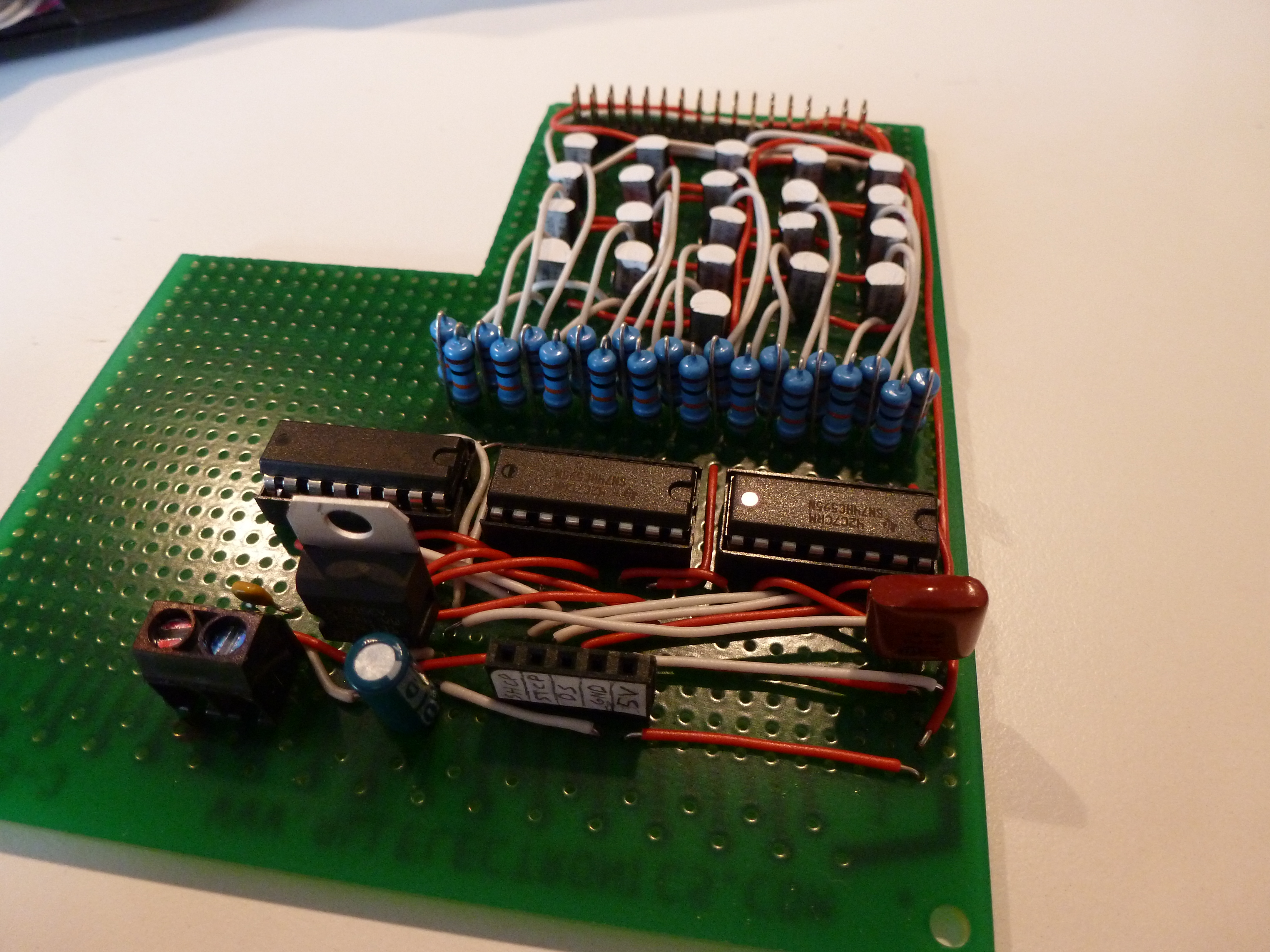
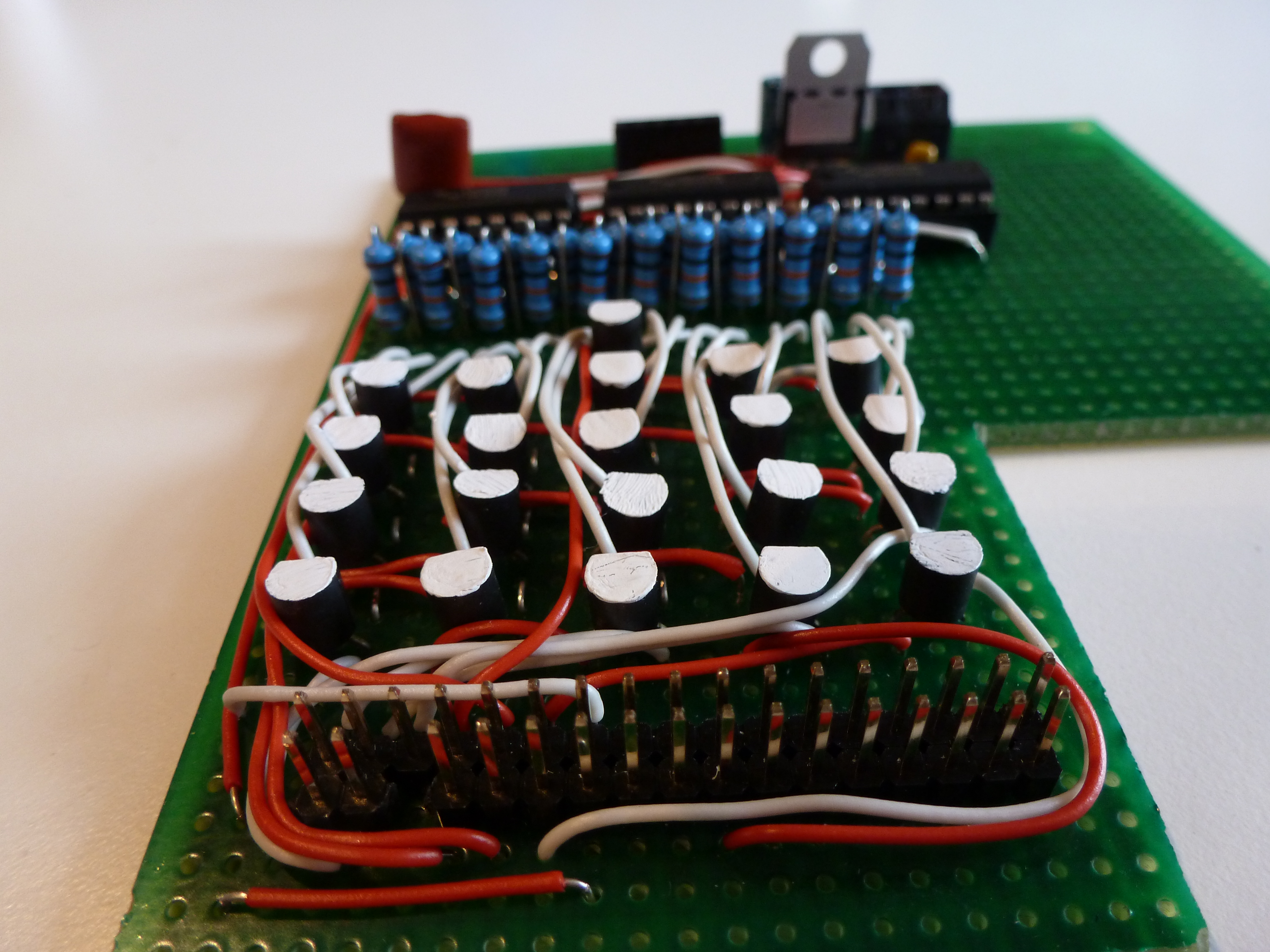
The last step is to round up the circuit with inputs for power, a voltage regulator (optional) and some connections.
- Add female headers to the circuit featuring connections to DS, ST_CP, SH_CP, Ground and Vcc of the circuit.
What voltage is the circuit going to run on?
I recommend 5V and taking the battery out. Even though the battery is rated at 3.7V, my cellphone ran more than fine on 5V.
- If you want to run the circuit off of batteries or an unregulated power supply, add a 5V voltage regulator like a 7805. Check the datasheet of the voltage regulator for a schematic. It should be very simple and often only involves 2 capacitors.
- You must make some more connections if you haven't yet: Attach the ICs to the power supply and connect the power rails to the pinheads of the ribbon cable so the cellphone gets power as well. If you are running the cellphone off it's own battery, you must only connect the cellphone's and the circuit's grounds together.
In the first picture you can see the front of the circuit with: A screw terminal for unregulated voltages, a voltage regulator and a female header row with connections for the Shift register inputs and regulated 5V.
The other pictures are shots of the circuit from different angles.
Testing the Circuit
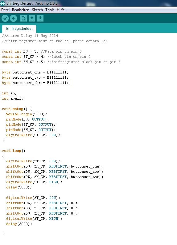
Now it's time for your arduino.
Above you see the program to test the shift registers.
Here's an explanation of some parts of the code:
- 'buttonset_one', '.._two' and '.._three' are the states the shift registers' outputs will be set to. Each shift register has 8 outputs, so each buttonset is one byte long. The 'B11111111' will therefor set all outputs to 5V.
- By setting 'ST_CP' to low, we disable the outputs while we shift the data through them.
- 'shiftOut' is called three times, one time for each shift register. Due to how a shift register works, 'buttonset_one' will be in the shift register at the end of the chain and 'buttonset_three' will be in the shift register connected directly to the arduino. 'MSBFIRST' stands for "Most significant bit first". If we were to send the bitset B1001100, the 1 on the left would be sent first. If the parameter would be 'LSBFIRST', the 0 on the right would be sent first.
- In this program we turn all outputs of all shift registers on, then wait 3 seconds, turn them all off again, wait 3 seconds, and repeat.
Load this program onto your arduino and connect it to your circuit. Take your multimeter and see if all outputs of the shift registers are at 5V. If they are not, make sure you waited longer than the 3 seconds they are turned off due to the program.
If the problem still exists, try to find it and solve it yourself. No one knows better than you what you soldered to your perf board. I can still try my best at helping you if post your problem in the comments.
From Here
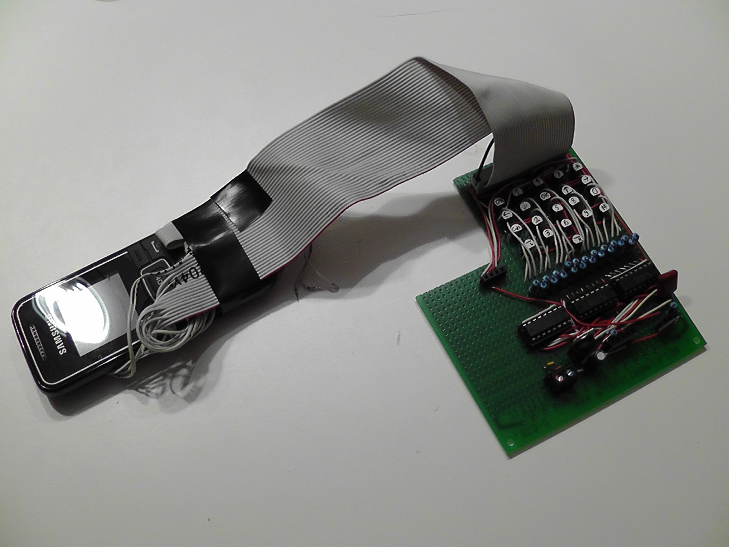
Now you have a device which can autonomously send data through texts via the cellular network to another phone.
Possible modifications:
- Using comparators, the microcontroller can read whether the speaker or the motor are on. This enables you to respond to a call or a text to the modded cellphone.