Tim's PCB (Plotted Circuit Board)
by Palingenesis in Circuits > Electronics
10742 Views, 46 Favorites, 0 Comments
Tim's PCB (Plotted Circuit Board)
This is the process I use to create a custom Circuit Board for my projects.
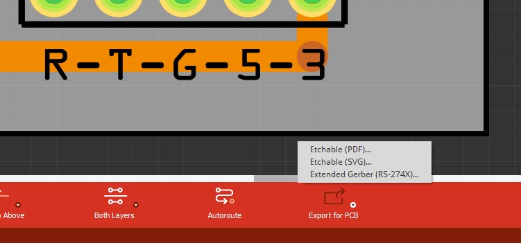
To make the above:
I use my XY Plotter with a Scribe to remove an etchant resit film to expose the copper to the etchant.
I use my XY Plotter with a Laser to burn ink into the top surface.
I use my XY Plotter with a handcrafting drill to drill the holes. (0.8mm)
It's a Process
This is how I do it:
I am not going to go into detail of how to use the programs I use, instructions on how to use the programs can be found on there relevant sites. What I will be doing is explaining the Process, and any tips to aid in the programs. At first glance this may look a bit longwinded, but once done a few times, its just click click click …
Create a Circuit Board Using Your Prefired Editor
First I create the circuit in Fritzing. Fritzing is a good program if you want to prototype using a Breadboard or Perfboard.
Update: I have now started to use KiCad, this is a set of Open Source applications. KiCad boards can be imported into FreeCAD.
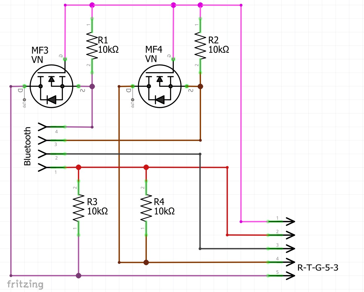
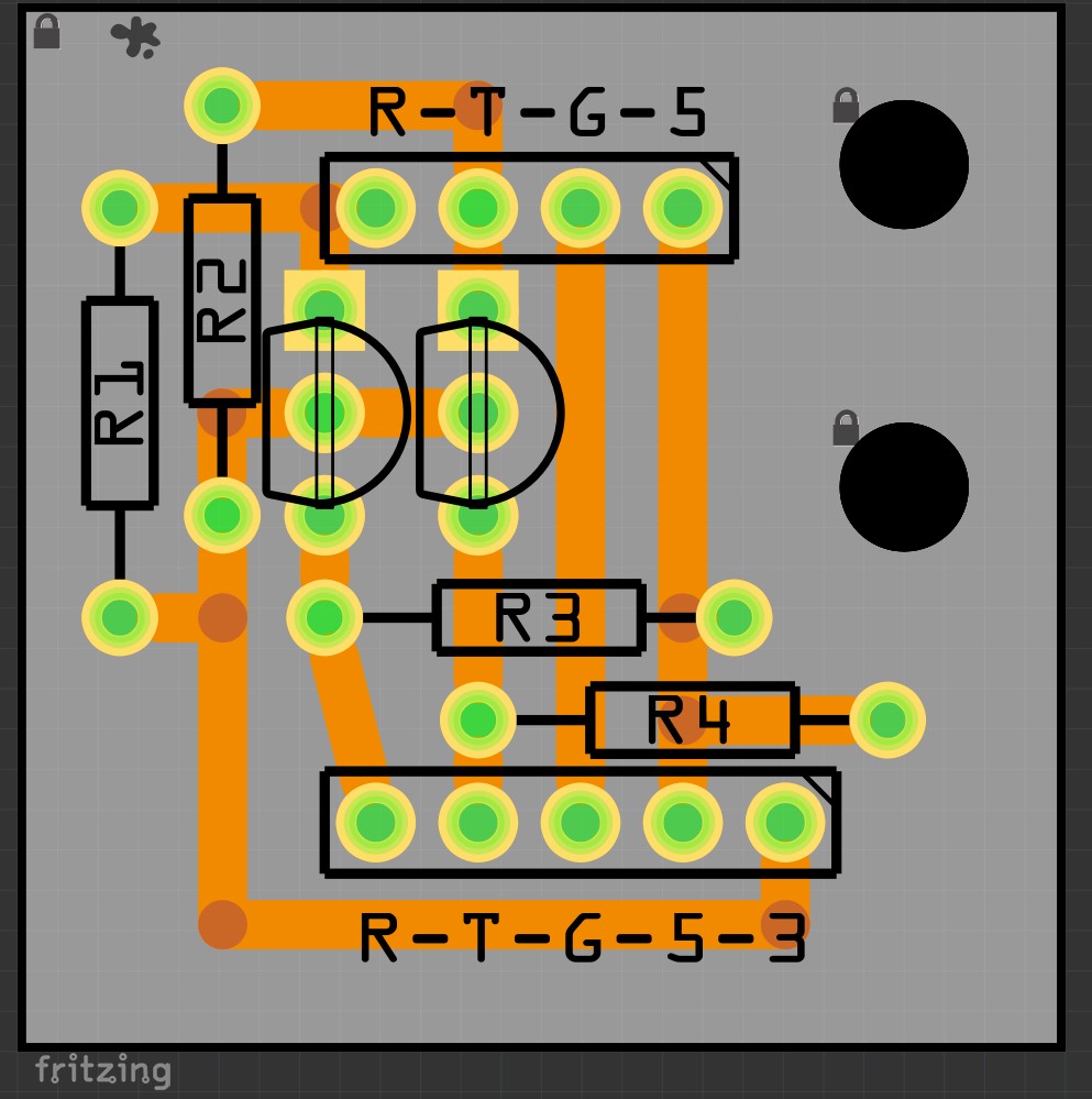
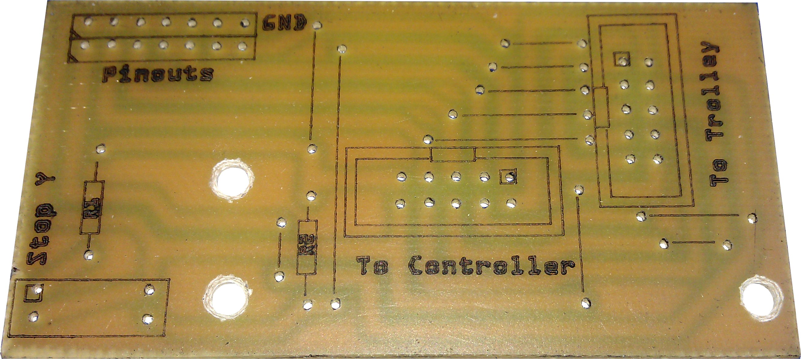
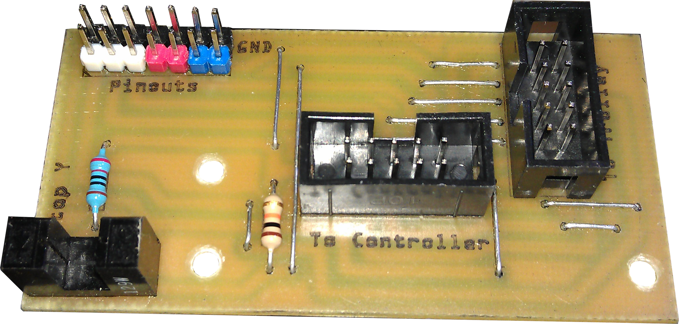
This is a small example board I made to show this process, it's a board I use to connect my Bluetooth Device to my Arduino. It shifts data 3.3v to 5v and 5v to 3.3v.
Export Relevant Files
Then I Export the PCB in "Extended Gerber (RS-274X)" and "Etchable (SVG)" To my projects folder.
I now have files I can convert to something my plotter can use.
File for the Scribe
The first file I need is the one to scribe the copper traces on the copper side of the board. (Expose Etchable Areas)
To do this I use FlatCAM.
FlatCAM Step 1
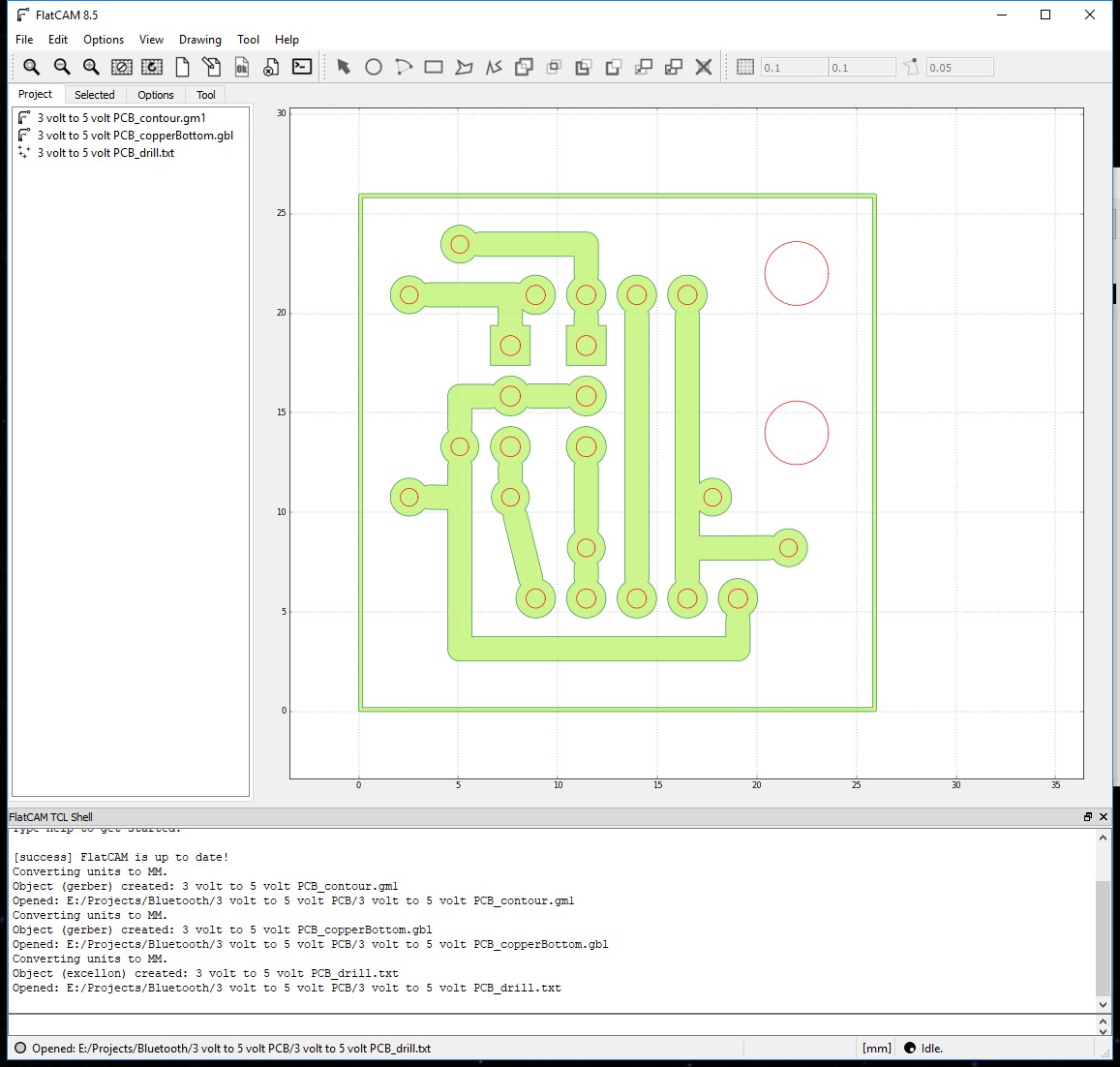
From the File menu, navigate to the project folder:
Open Gerber files: ???_contour.gm1 and ???_copperBottom.gbl
Open Excellon File: ???_drill.txt
FlatCAM Step 2
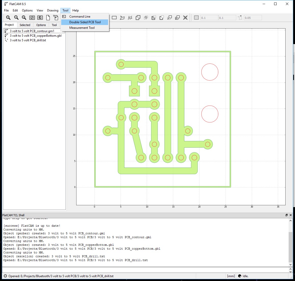
These are viewed from above, so they need to be flipped. (I preferer to flip them horizontally)
Select Tool from the top menu, the choose Double-Sided PCB Tool.
FlatCAM Step 3
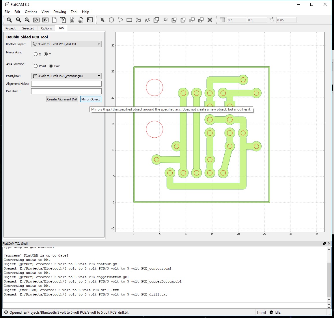
In the Tools window set:
Mirror Axis to "Y", Axis Location to "Box" Pint/Box to ???_contour.gm1 (this is the size of the board, so it set the area to flip things)
Bottom Layer is the files to be flipped.
Choose: ???_copperBottom.gbl then click Mirror Object.
Choose: ???_drill.txt then click Mirror Object.
FlatCAM Step 4
Next is to create the geometry for the path the scribe will take.
I do both the copper traces and the holes. (The reason for doing the holes, is when they are etched, they act like pop marks for the drill bit )
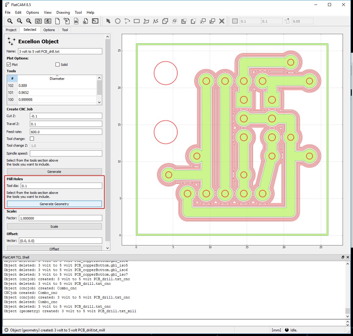
FlatCAM Step 5
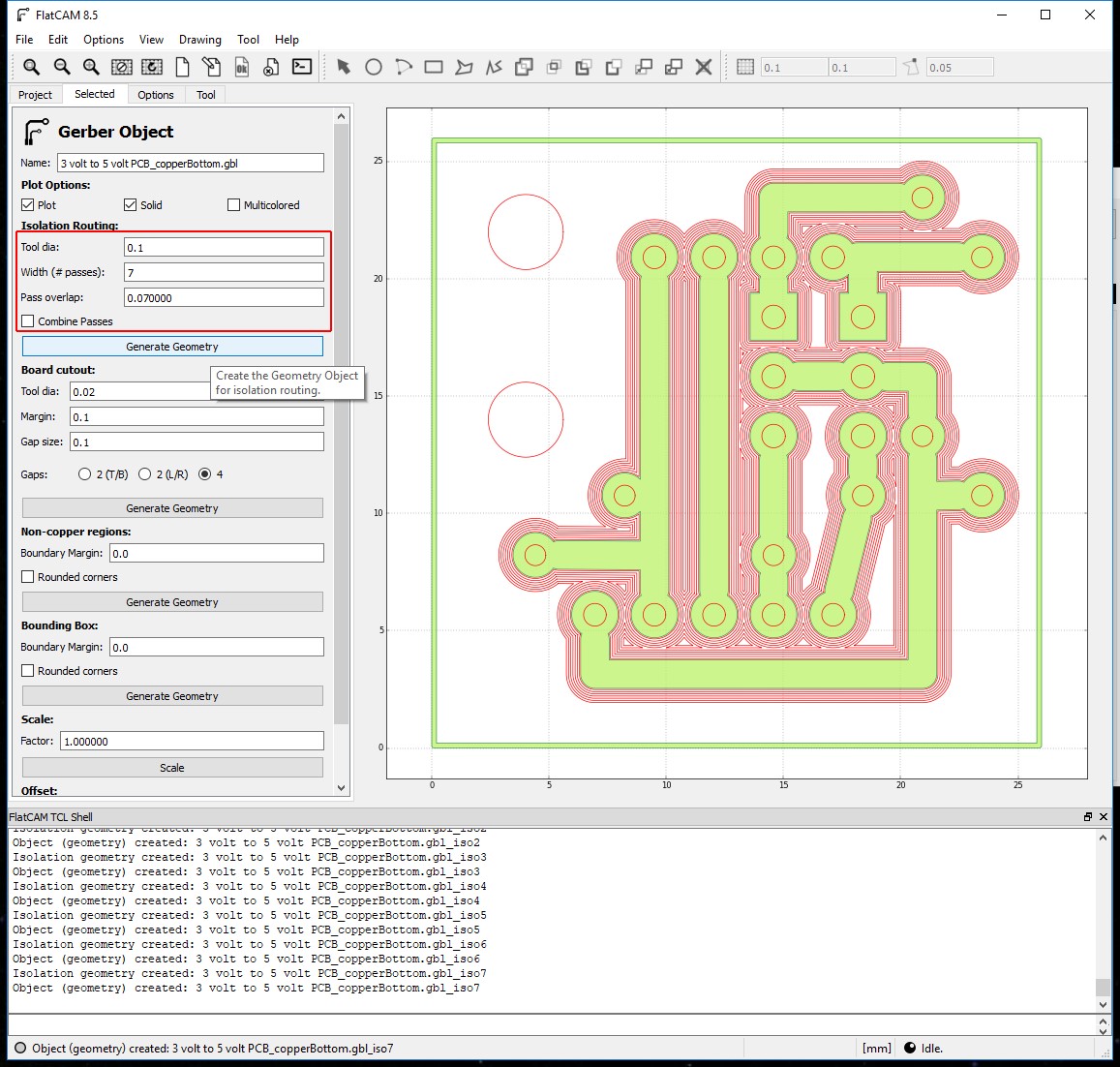
So, in the "Project" Tab select: ???_copperBottom.gbl file, then select the "Selected" Tab.
Set the settings shown in red border and click "Generate Geometry" for Isolation Routing.
Notice that the Combine Passes is not ticked. (I will be combining things later)
FlatCAM Step 6
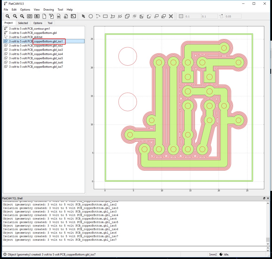
The reason I did not combine passes, is because I want to remove the first pass. (the reason is a bit long winded, so I won't explain at this time.)
Go back to the "Projects" Tab and delete the first pass.
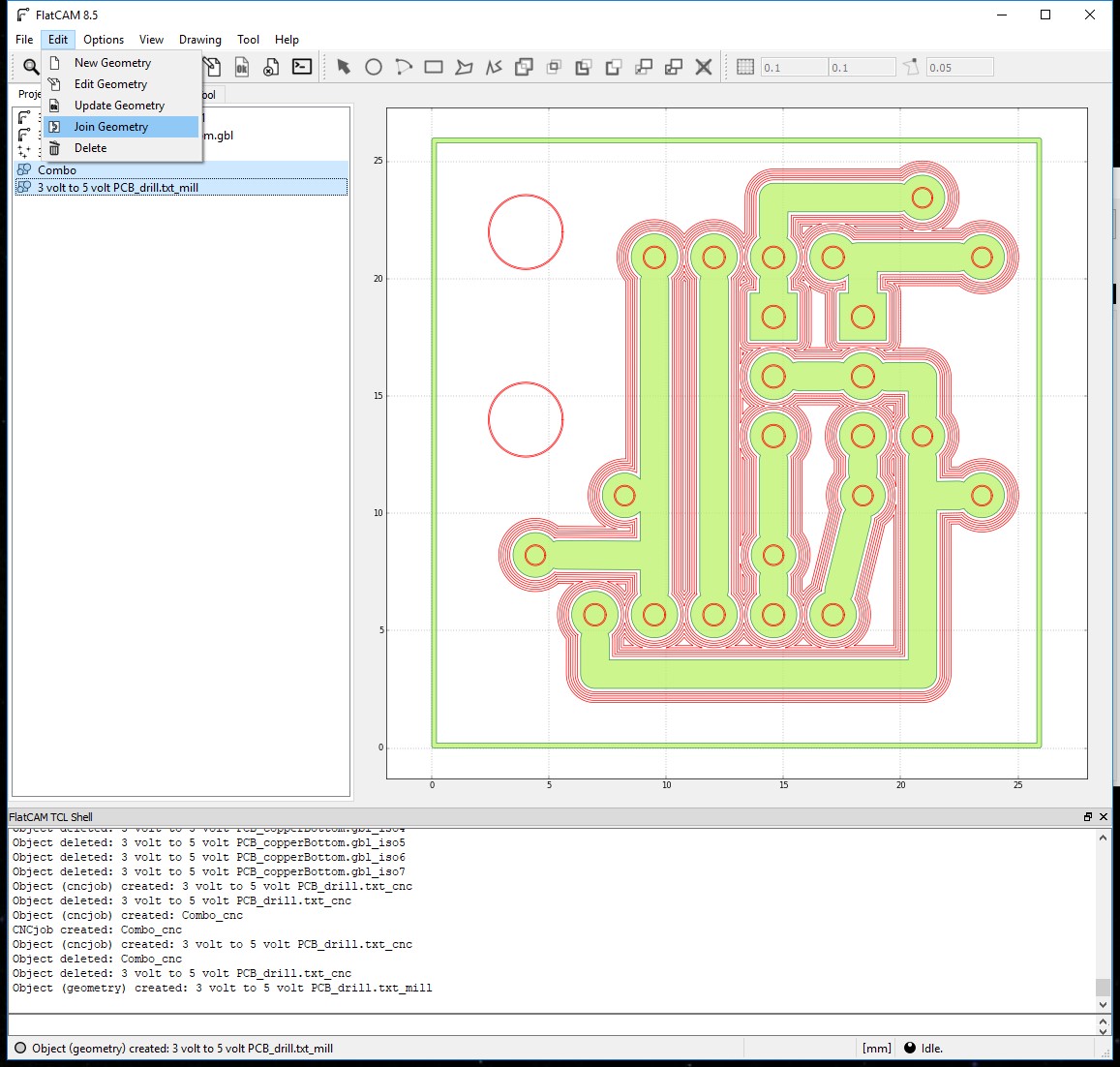
FlatCAM Step 7
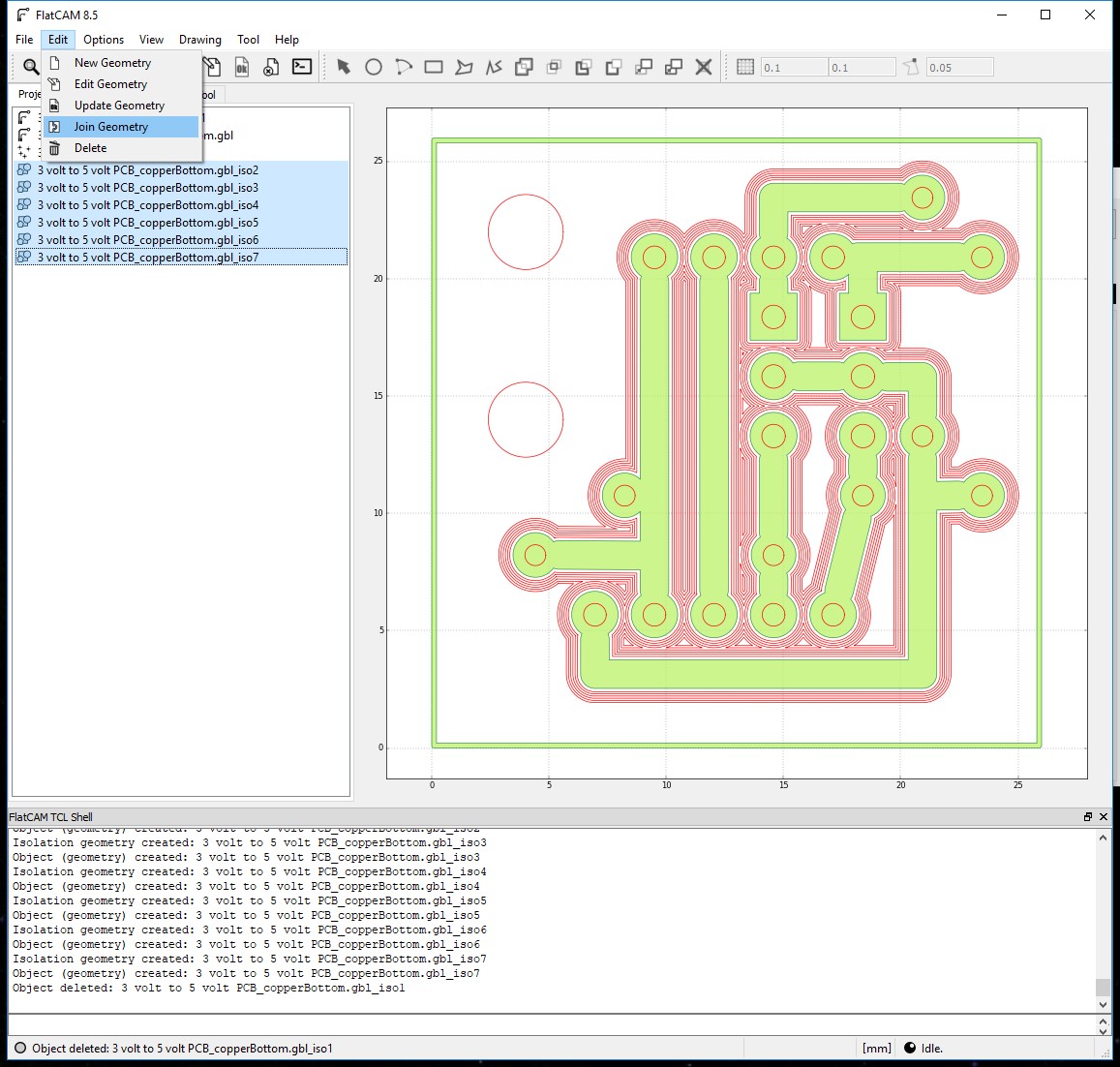
Select the remaining paths and select "Edit" from the main menu and chose "Join Geometry"
This creates a new file: "Combo".
FlatCAM Step 8
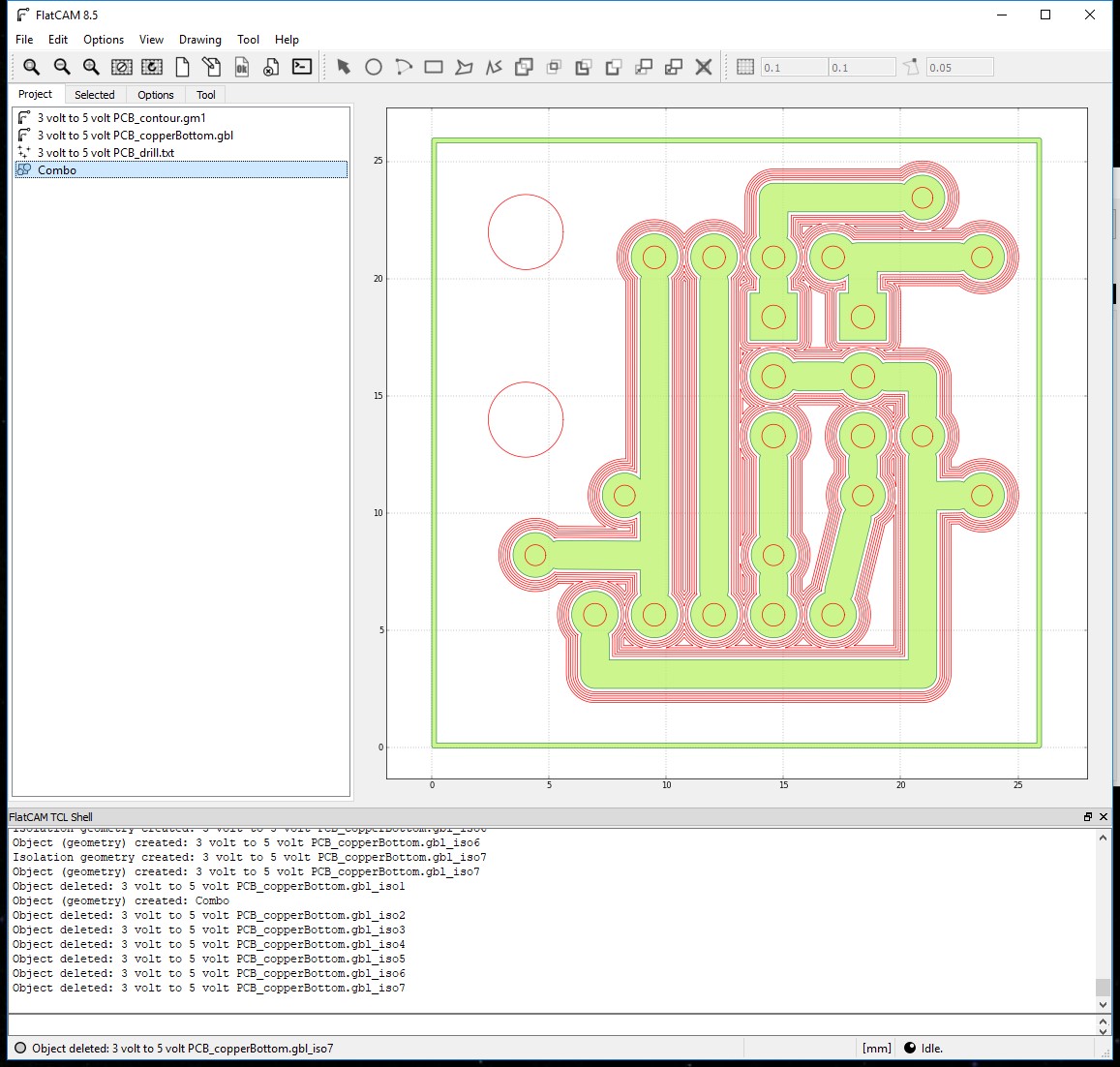
So the original paths can be deleted.
FlatCAM Step 9
I like to etch the holes to aid the drilling process, so paths are needed for the holes.
To do this, in the "Projects" Tab, select the ???_drill.txt file and then select the "Selected" Tab.
With the settings shown in the red border, click "Generate Geometry" for Mill Holes.
FlatCAM Step 10
Before the next step both path files can be joined.
In the "Projects" Tab, select the 2 path files and select "Edit" from the main menu and choose "Join Geometry"
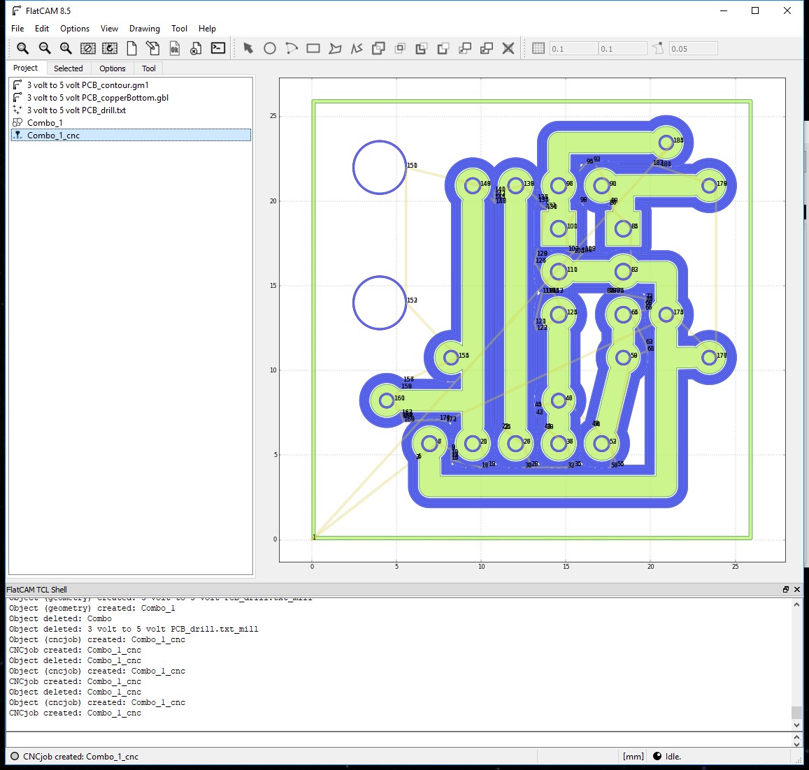
FlatCAM Step 11
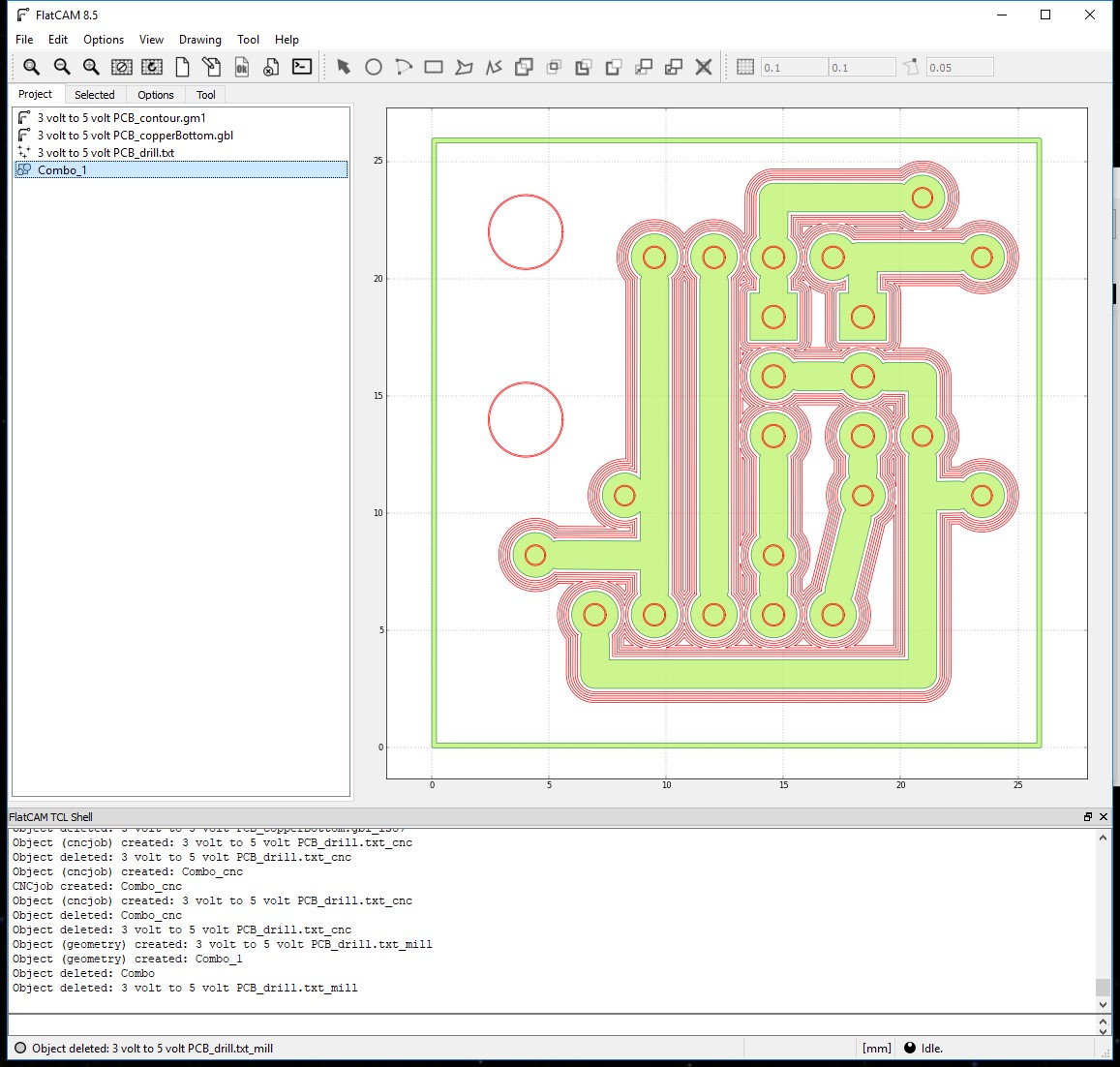
This creates a new file: "Combo_1".
So the original paths can be deleted.
FlatCAM Step 12
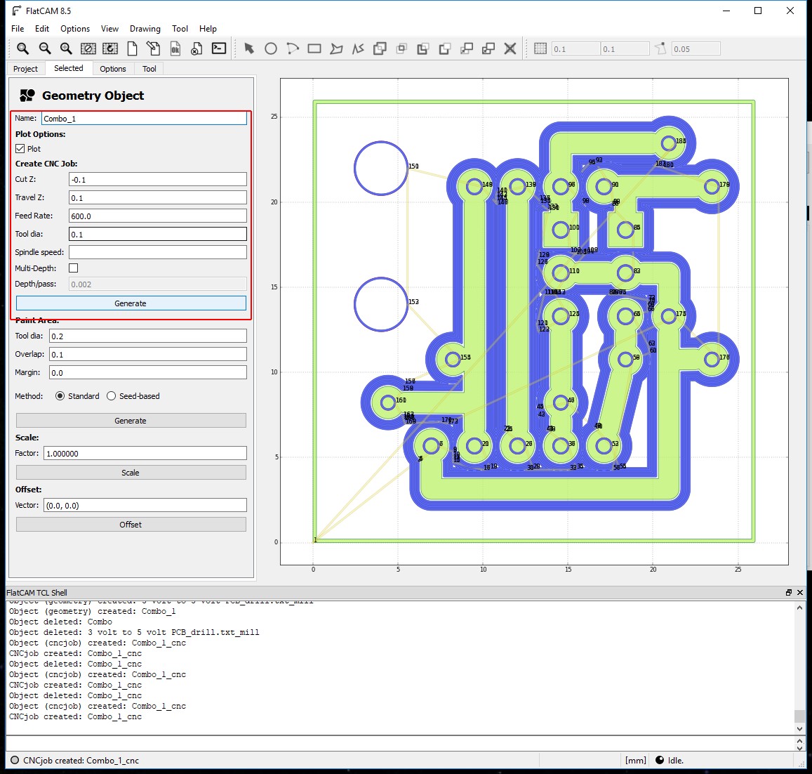
Next, select that new combined path file (Combo_1) and select the "Selected" Tab.
Set the "Tool dia" as shown in the red boarder.(this is drawn in blue when "Generate" is pressed)
The other settings are plotter (machine) dependant.
They don't matter to me, as I am going to edit the final G-Code produced later.
Click the "Generate" button.
This creates a new CNC file.
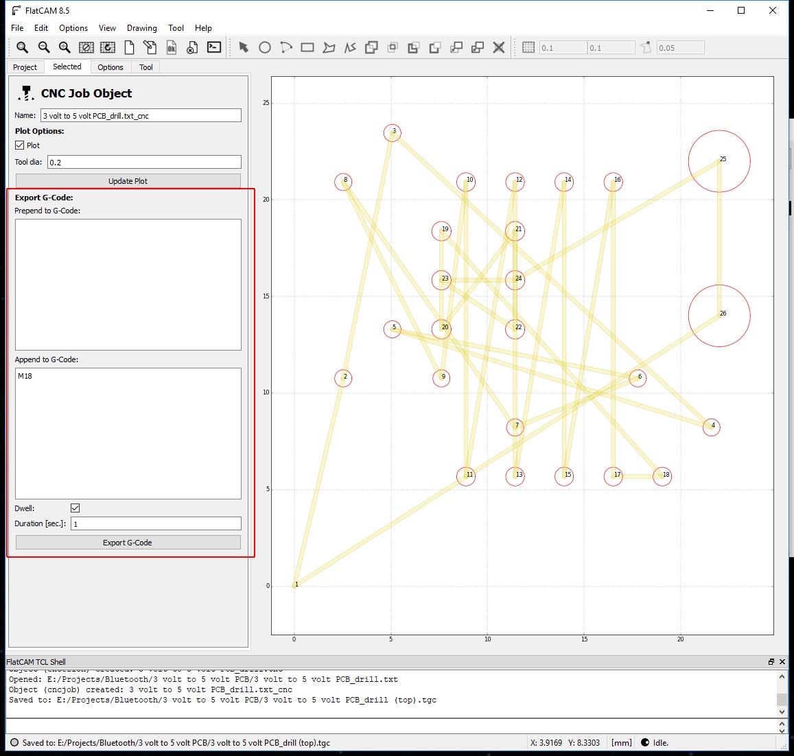
FlatCAM Step 13
Go to the "Projects" Tab and select it.
FlatCAM Step 14
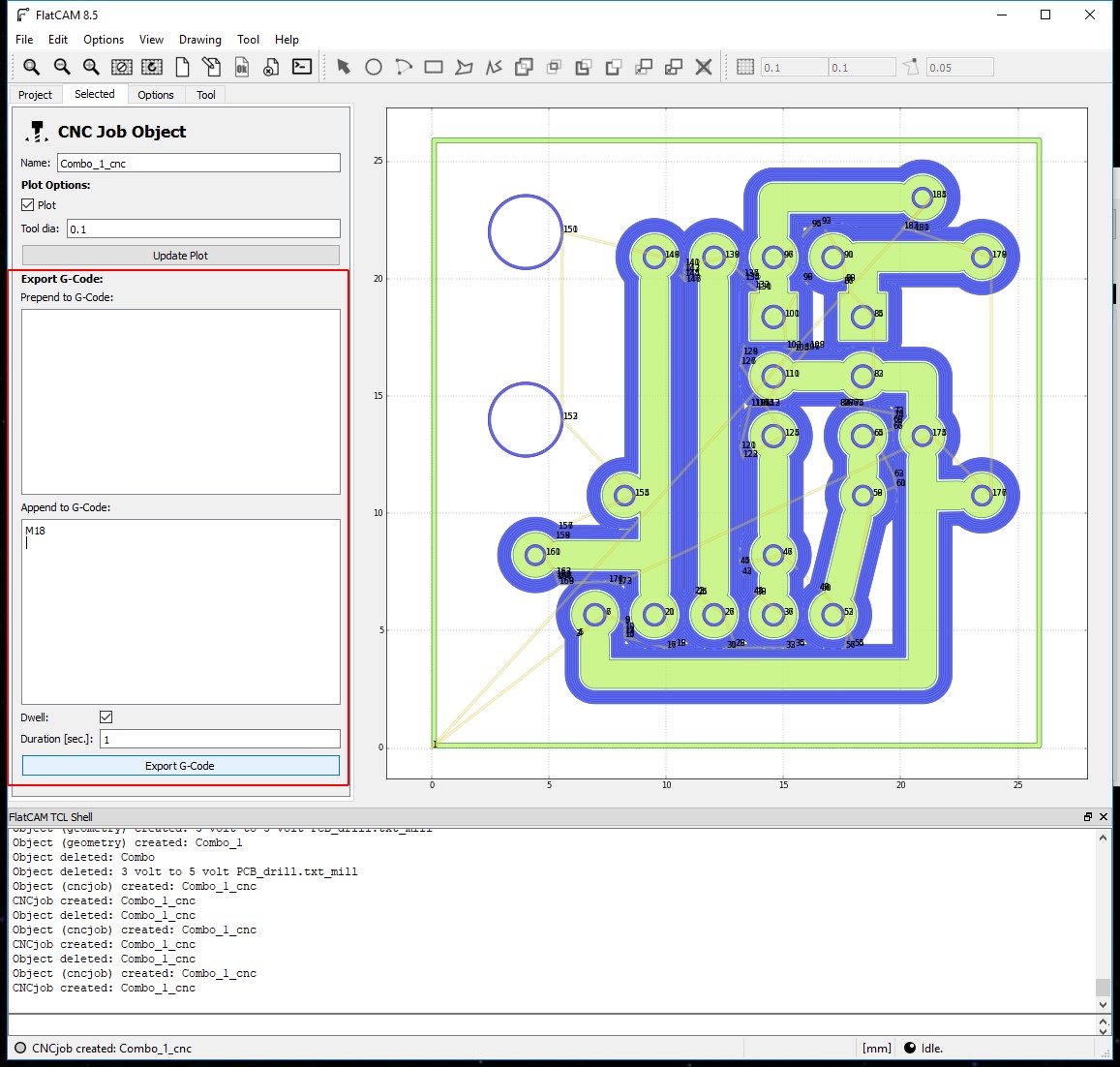
Go to the "Selected" Tab.
Here is where the file is exported to G-Code.
At this point commands can be prepended or appended to the code produced.
I add M18 to turn off the motors when finished.
Click "Export G-Code"
I give the file name the same as the ones produced in Fritzing with my own file type.
e.g. ???_copperBottom (with holes).tgc
If it is going to be used with a machine that runs CNC G-Code then use the file type .gcode
This file is the one used to control the scribe.
The XY Plotter I am using is one I have designed and built myself, so the firmware and software used is what I have written.
So I will be editing this file so that my firmware understands it. (it's still based on G-Code)
File for the Drill
Next I need a file for the drill.
For this I use the ???_drill.txt again.
I delete every thing else from the "Project" Tab. (remember this one is a flipped one, so if you delete it and reload it, you must flip it again)
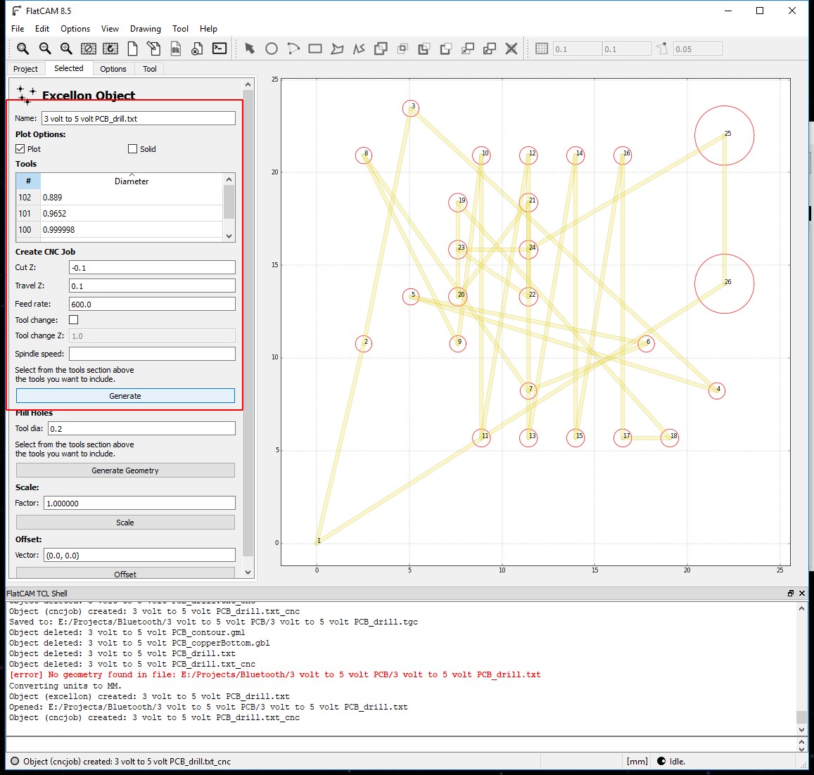
Select the ???_drill.txt file and select "Selected" Tab.
This time I create a CNC file.
Click "Generate" Button.
The settings here in the red boarder are plotter (machine) dependant.
They don't matter to me, as I am going to edit the final G-Code produced later.
FlatCAM Step 15
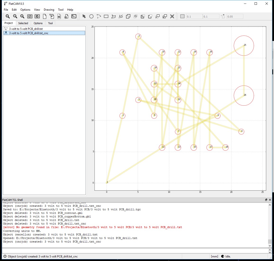
Next select the "Project" Tab and select the new ???_cnc file
FlatCAM Step 16
Then select the "Selected" Tab and export to a G-Code file as before.
This file will be named ???_drill.tgc (file type dependant on machine used)
This file is the one used to control the Drill. I will be editing this file so that my firmware understands it.
I also need a file to align my plotter when I turn over the PCB to draw the component locations on the top side.
I make another drill file as I have just done but with a reload one and don't Flip it.
I name it ???_drill (top).tgc (I will explain later).
I have now finished with FlatCam.
Currently I have produced 3 files:
???_copperBottom (with holes).tgc
???_drill.tgc
???_drill (top).tgc
File to Draw Component Locations
Next is creating a file for the top. (To draw the component locations)
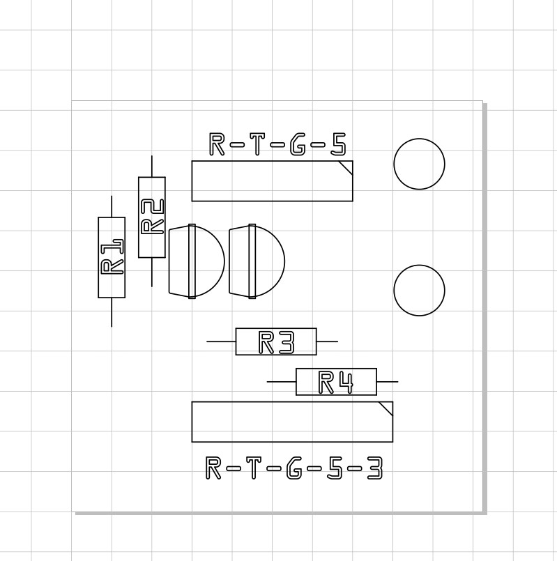
To do this I use the ???_etch_silk_top.svg file in my project folder created by Fritzing.
This is a Scale Vector Graphics (SVG) file, so can be edited with any program that can handle this type of file.
e.g. Inkscape, I haven got the hang of layers in ink scape yet, so I use Corel Draw and export it.
This file contains several layers, I don't want to use them all, so I edit is to that it only contains what I want and save it as new file. (e.g. ???_etch_silk_top (modified).svg)
Edit SVG Step 1
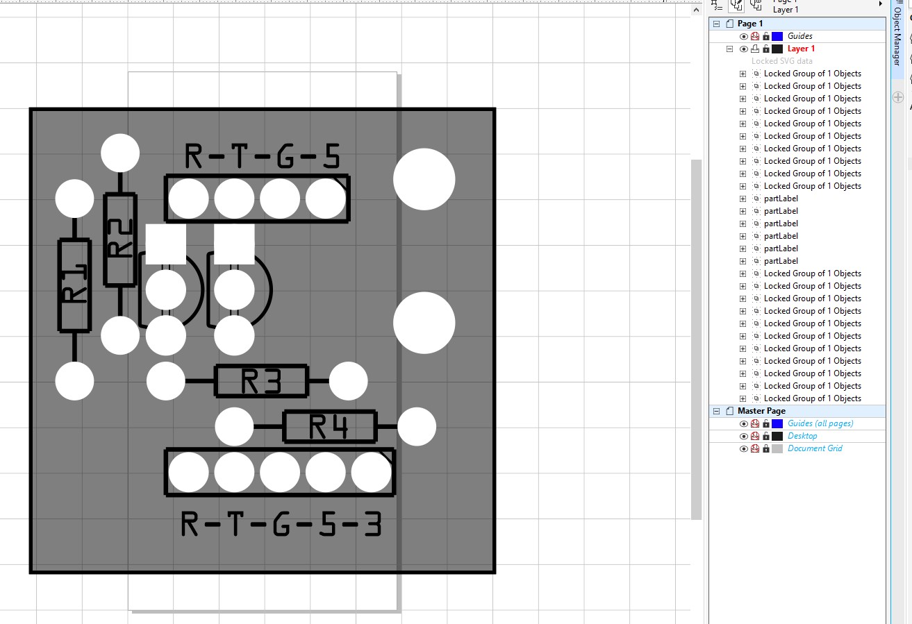
This is what the file looks like:
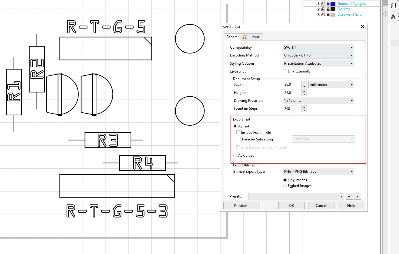
I have written a sub program in my software to convert SVG to G-Code (tgc) but there are addons for Inkscape that do it as well. (as I mentioned, I'm just showing my process of doing it)
Edit SVG Step 2
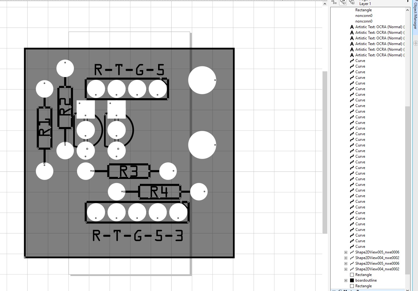
My software can't handle multi-subgroups so I need to simplify the file.
First I ungroup every thing.
Edit SVG Step 3
Then I make all objects "Hairline" and "No Fill".
Make the canvas the same size as the board. Make sure the board is aligned with the canvas.
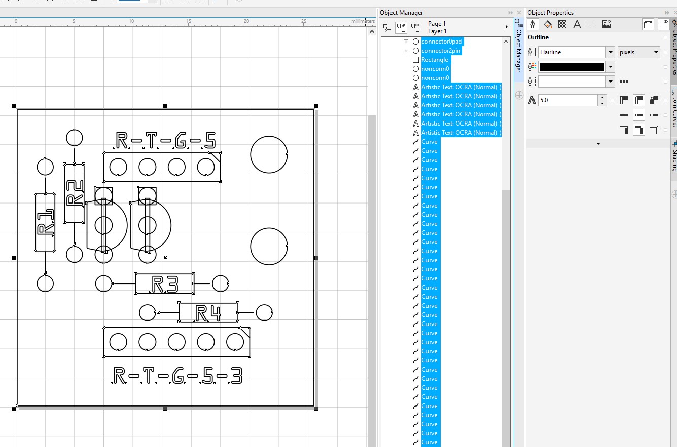
Edit SVG Step 4
Then remove every thing I don't want.
Edit SVG Step 5
As I am using Corel Draw, I export it as a SVG.
My SVG to G-Code program uses true type fonts (TTF) so I set the settings accordingly.
Convert to G-Code Step 1
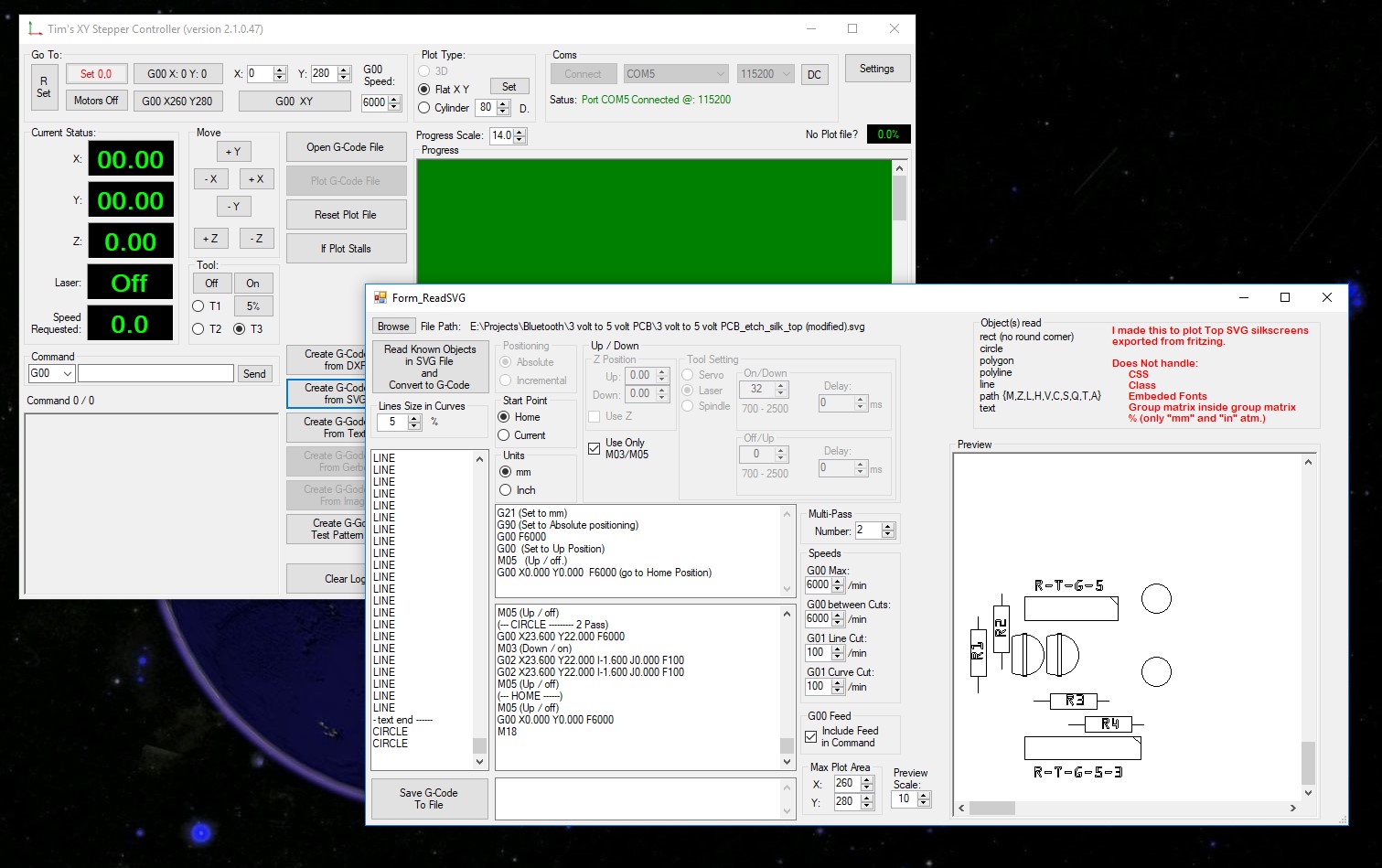
Now that I have the SVG file I need, I can convert this one to G-Code (tgc) with my software.(Tim's XY Controller)
This file can be sent to my plotter as is.
Convert to G-Code Step 2
Those familiar with G-Code files will know you can get variations on the original.
To give an example:
CNC G-Code. Take a look here: Understanding Common Fanuc Style
3D Printer G-Code. Take a look here: 3D Printer
grbl G-Code. Take a look here: grbl
If you have been wondering why I give my files, the file type .tgc? It's "Tim's G Code". My modification of G-Code.
I assume what ever Plotter you use, you have read the manual.
I need to edit the other 3 files so that my plotter understands them.
They are small edits, mostly gramma. I have one plot and two drill files to edit.
To edit the files I just use Notepad. I use the Edit => Replace (replace all) tool.
File Edits Step 1
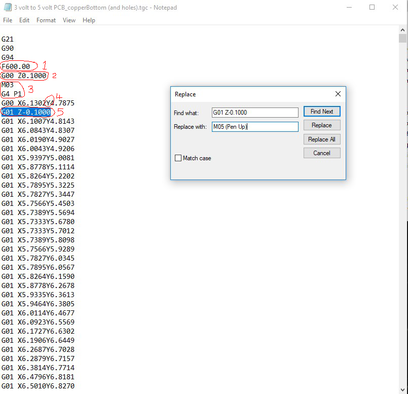
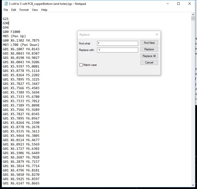
First file: ???_copperBottom (with holes).tgc
1. This is a feed speed command. I need to a G00 in front and set what speed I want. (once only)
2. This is a move command, move Z to a position above zero. As I don't have Z movement as such, I have a servo or laser, I need to change it to a off/up command, I have used the code M05 for this, so all these commands need replacing. (click replace all)
3. I need to remove these at this point. (once only)
4. My Firmware needs a space in front of the "Y". (click replace all)
5. This is a move command, move Z to a position below zero. As I don't have Z movement as such, I have a servo or laser, I need to change it to a on/down command, I have used the code M03 for this, so all these commands need replacing. (click replace all)
File Edits Step 2
After Editing.
The L700 in the command "M03 L700 (Pen Down)" is a level value, used to set the servo at a position or set the power of the laser.
Text in brackets are comments and are ignored by the firmware.
File Edits Step 3
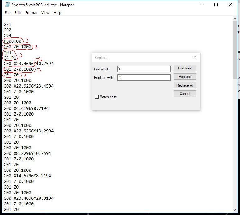
The drill files: ???_drill.tgc and ???_drill (top).tgc are a little different, there is a command to pause while the hole is drilled.
1. This is a feed speed command. I need to a G00 in front and set what speed I want. (once only)
2. This is a move command, move Z to a position above zero. As I don't have Z movement as such, I have a servo or laser, I need to change it to a off/up command, I have used the code M05 for this, so all these commands need replacing. (click replace all)
3. I need to remove these at this point. (once only)
4. My Firmware needs a space in front of the "Y". (click replace all)
5. This is a move command, move Z to a position below zero. As I don't have Z movement as such, I have a servo or laser, I need to change it to a on/down command, I have used the code M03 for this, so all these commands need replacing. (click replace all)
6. This is move Z to zero. I don't want this, I want it to wait while the hole is drilled. Here I replace it with the dwell command "G04 P5000 (Wait 5 seconds)". (click replace all)
File Edits Step 4
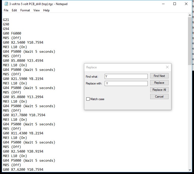
After Editing
I now have 4 files to use with my XY Plotter.
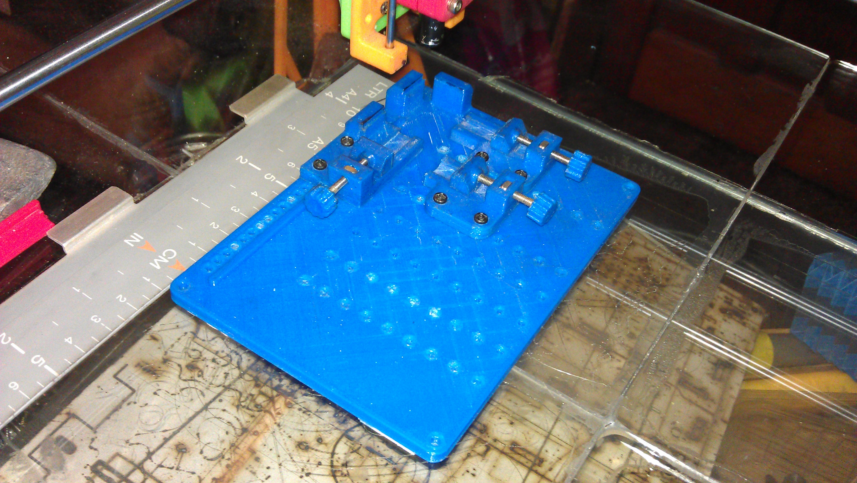
PCB Holder
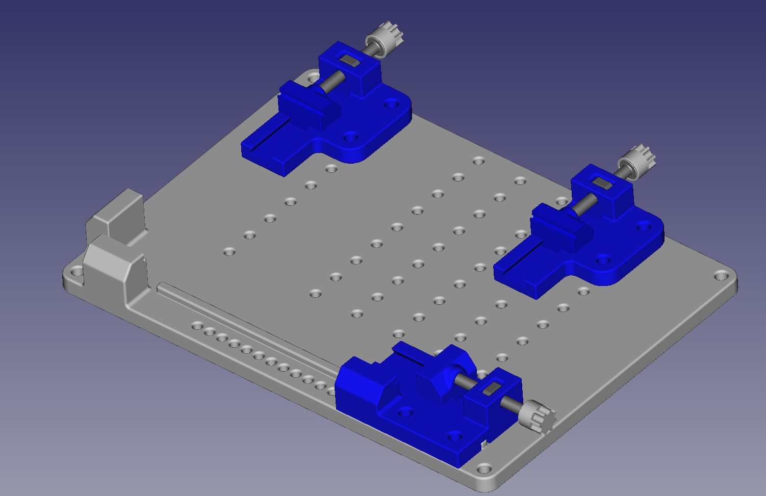
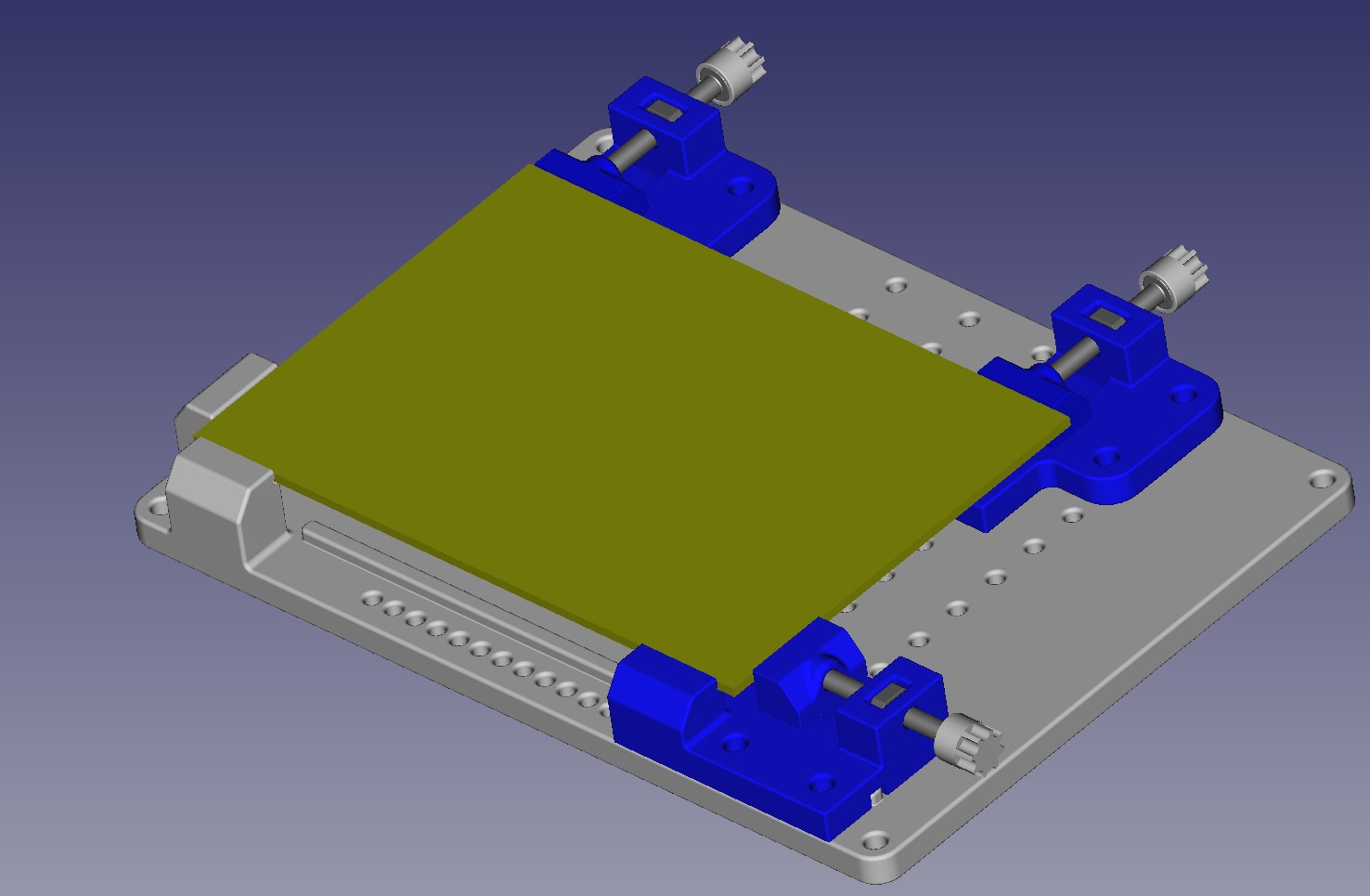
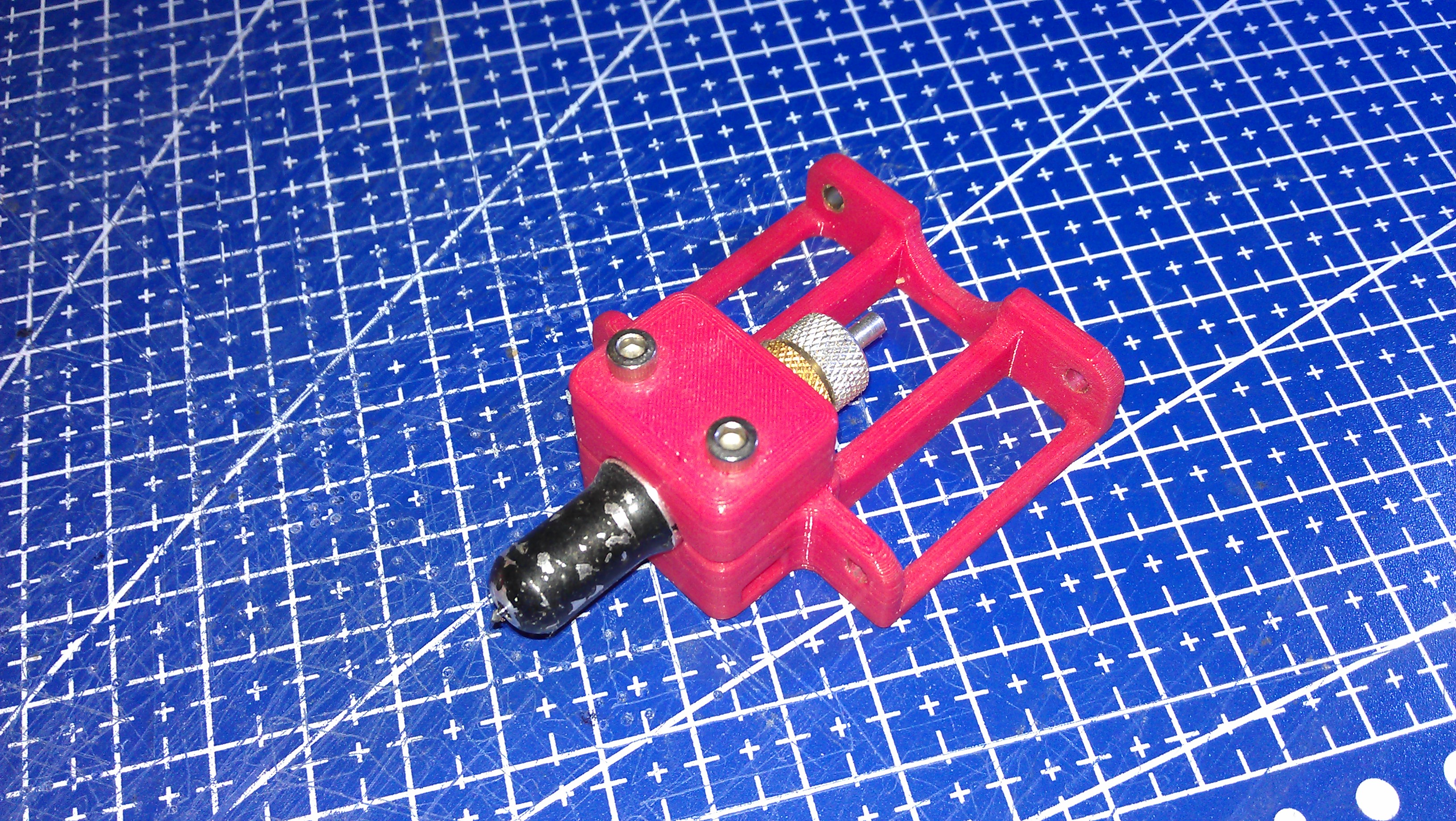
When scribing and drilling my PCB, I need something to hold it in place.
I have found that it is a good thing, if I can remove the PCB from the holder and replace it back in the same position it was removed from.
It also has to hold it above the bed, so that when drilling, the drill will not foul on anything.
I have come up with this design shown in the photos, I printed on my 3D printer.
I has 2 stops and support that are fixed, 1 stop with support and clamp that is adjusted along a guide to keep things parallel, 2 clamps with support that can be moved to many positions.
The nuts are M3 square nuts, the screws are M3x25mm hex head with grips fixed with 2 pack adhesive. It will take a board max size: 105mm X 75mm.
Here are the STL flies if you wish to make one:
Size the Board
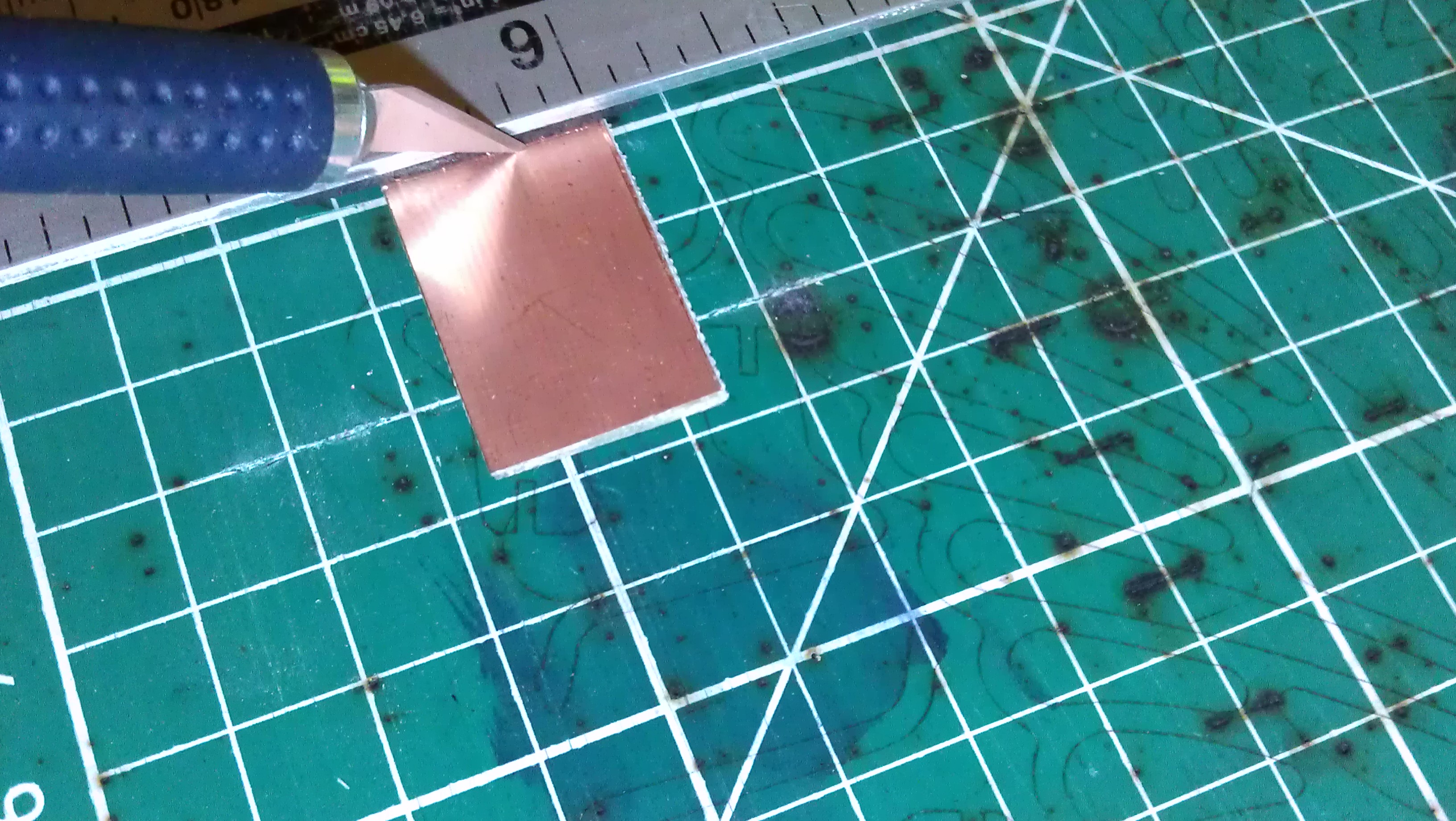
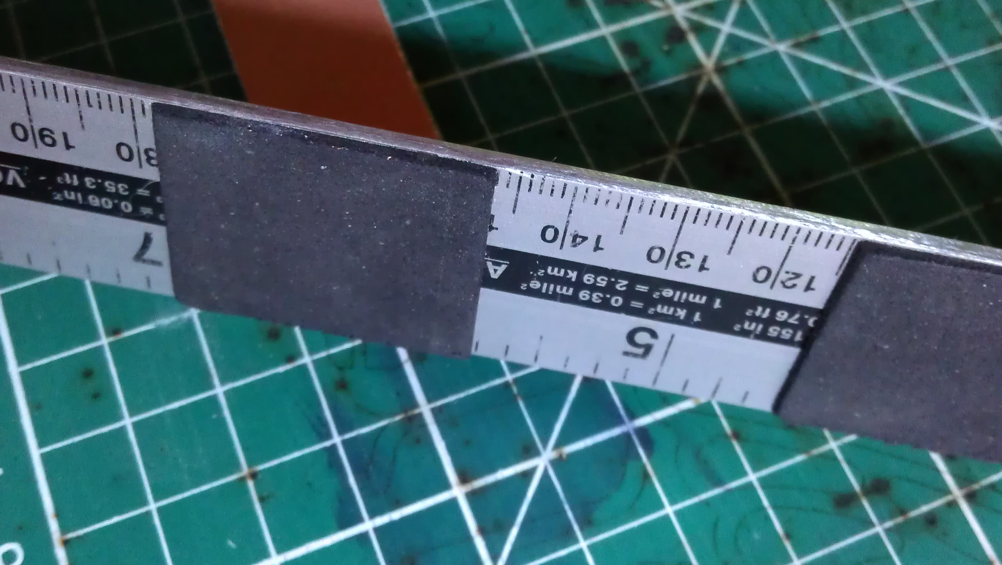
Next Cut the Copper Clad Board to size.
To do this, I just score both sides with a crafting knife and snap it two.(some times its best to snap it over a straight edge)
I use the back side of the blade to score, I find it scores better and does not wander off as much.
I also have stuck foam pads to the underside of my rule, it stops it sliding about.
Prepare the Board
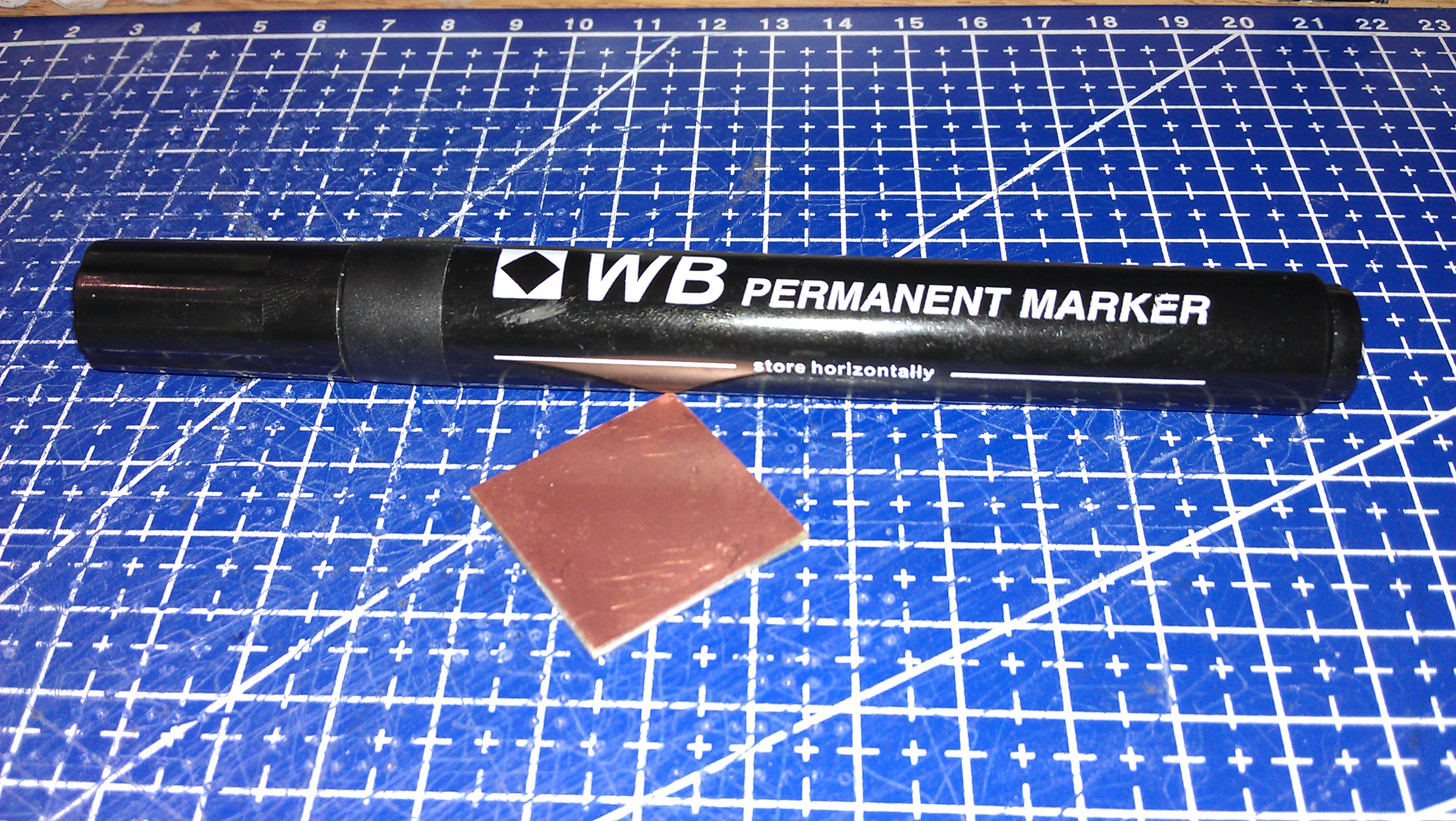
As I have stated, I am going to use a Scribe to remove an etchant resit film to expose the copper to the etchant.
The etchant resist is just ink from a Chisel Tipped Permanent Marker Pen. (a permanent marker is water resist, so it is also Ferric Chloride resist)
Coat the Copper Side of the Board with ink, using the Chisel Tipped Permanent Marker Pen. (I use a chisel tipped pen because it coats it easier)
Make a Scribe Step 1
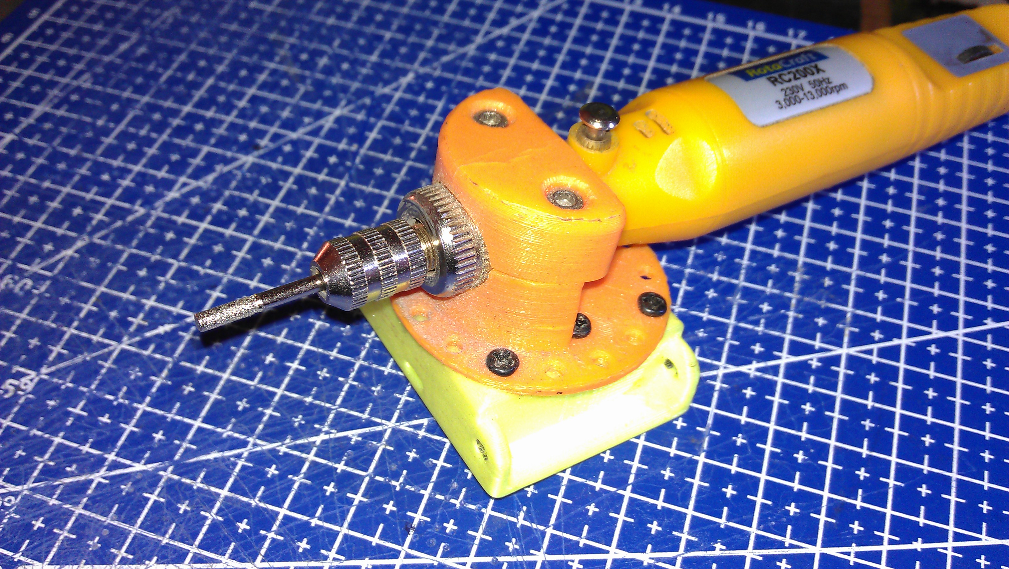
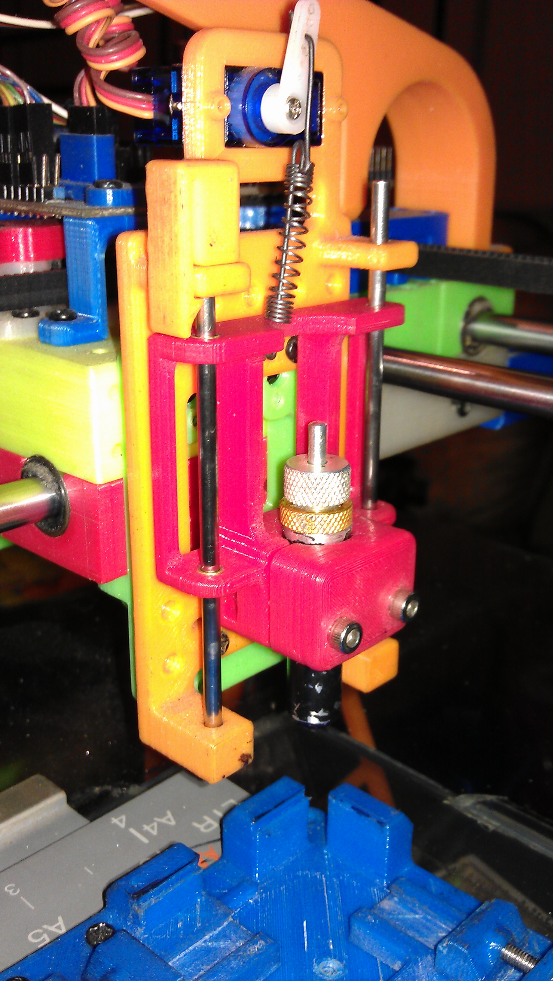
There are no Scribes on the market that I know of, to do what I want to do, so I have had to make one.
There is however a knife on the market for cutting vinyl.
Make a Scribe Step 2
I have made an attachment for this that fits on my XY Plotter.
I cannot use this as it stands. If I was to use a knife blade it would dig into the copper and possibly jam. I don't want this. I don't want to damage the copper.
One thing that is good about this process is:
If I realize I have made a mistake in the circuit before etching, all I have to do is coat the board in ink again and reuse the board.
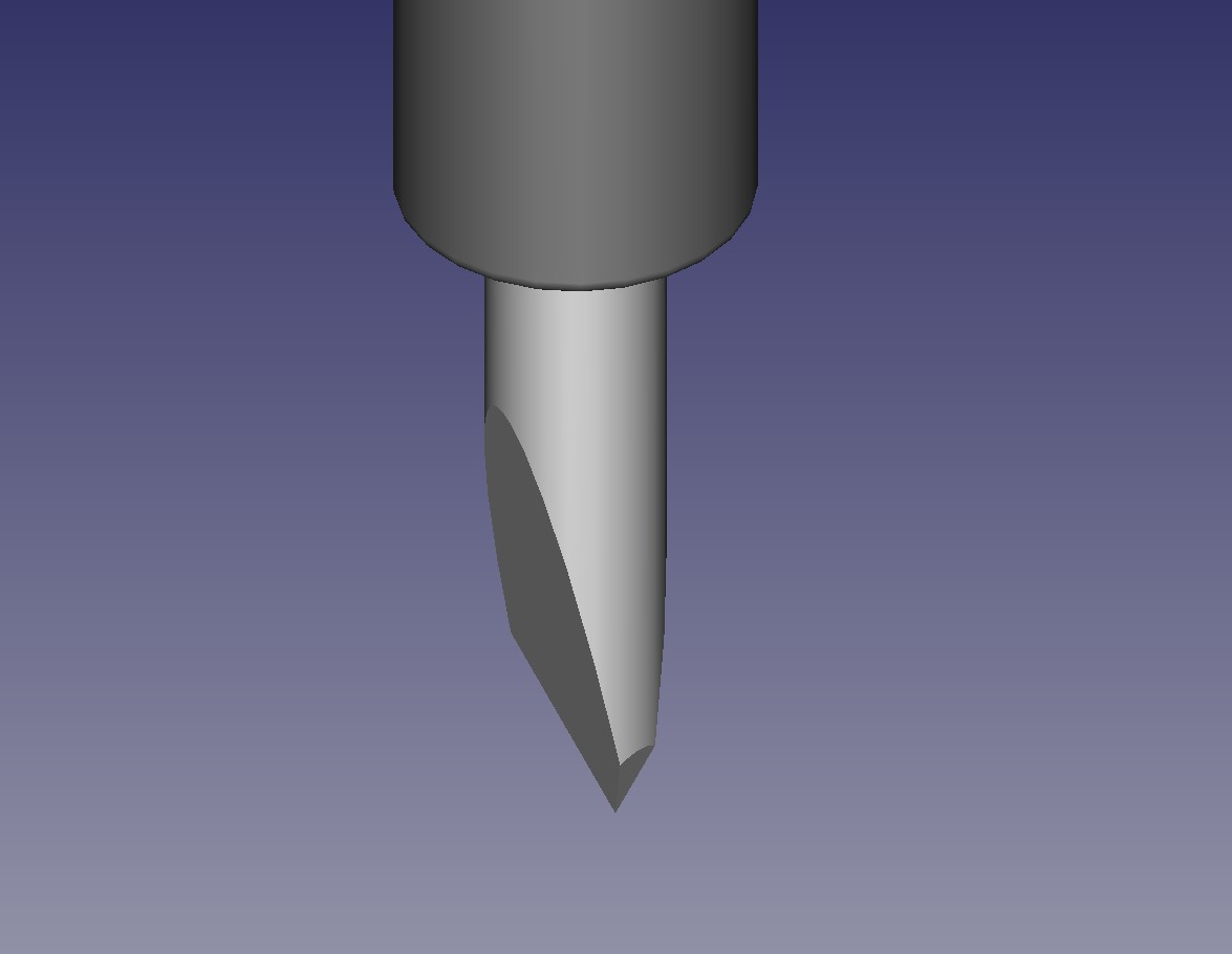
So, I took an old knife and reshaped it into a scribe, it has a flat end so it just sits on top of the copper but has a square sharp face on its leading edge to scrape away the ink.
Make a Scribe Step 3
Reshaping one of these blades is not easy by hand but is possible, I did it.
You will need a rotary tool with a diamond bit to do it, the knife blades are made of very hard stuff.
Make a Scribe Step 4
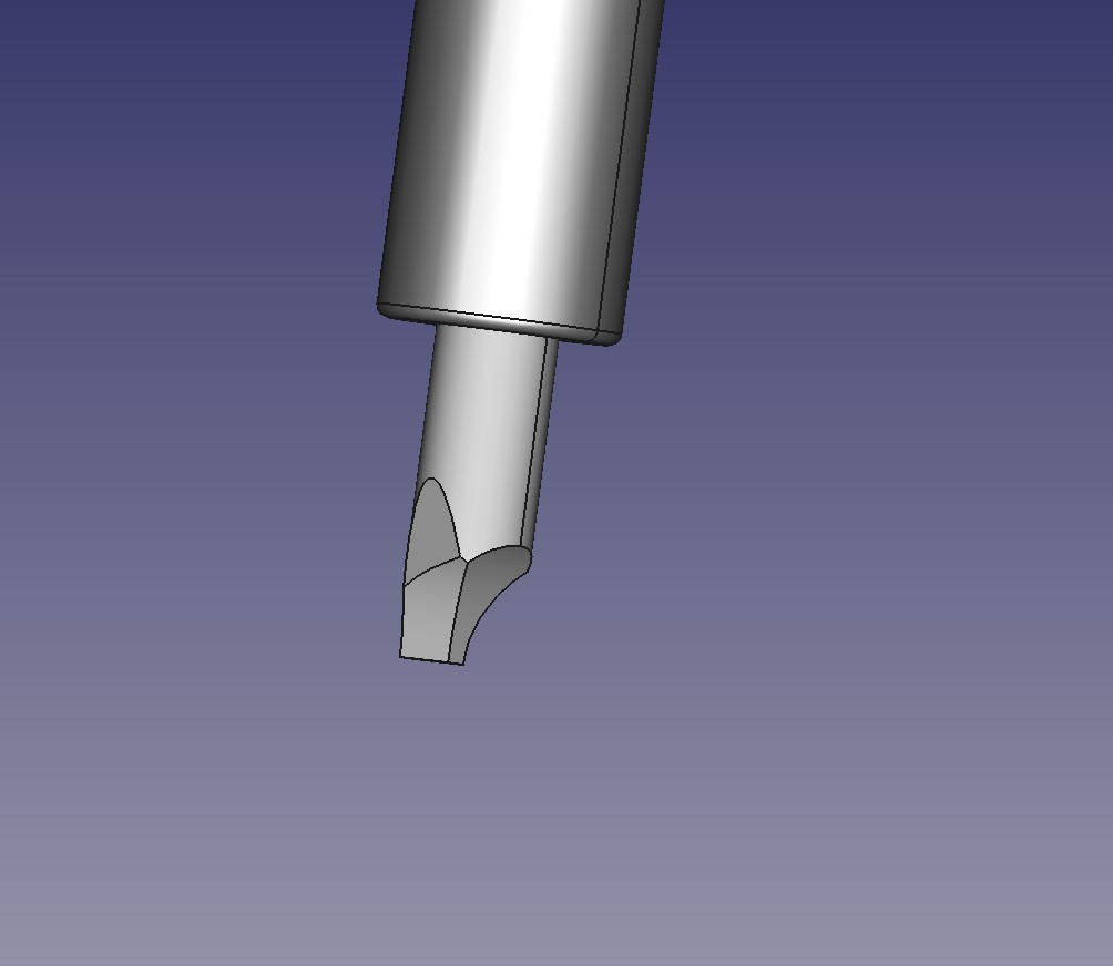
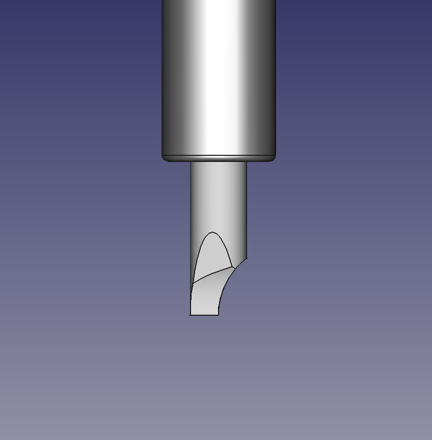
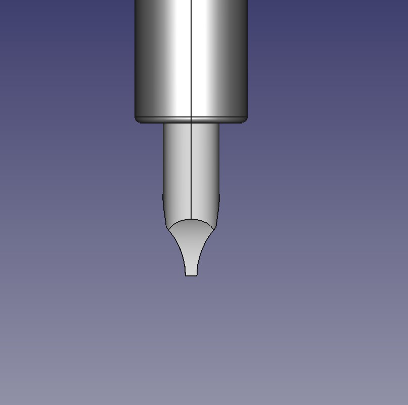
First picture is original shape, others are different views of the shape I made Scribe.
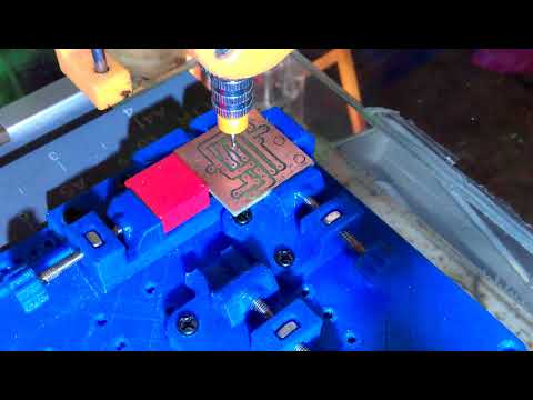
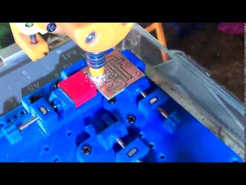
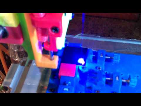
Scribe the Board Step 1
Once I had made the Scribe, I set up my XY Plotter.
Scribe the Board Step 2
The tool holder needs to be spring loaded. (using a fixed Z Axis will be difficult to adjust, as we are removing the thickness of ink)
Scribe the Board Step 3
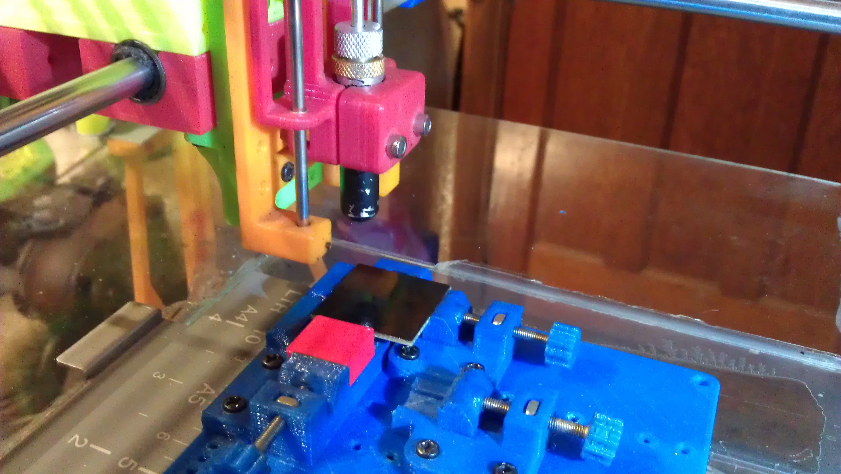
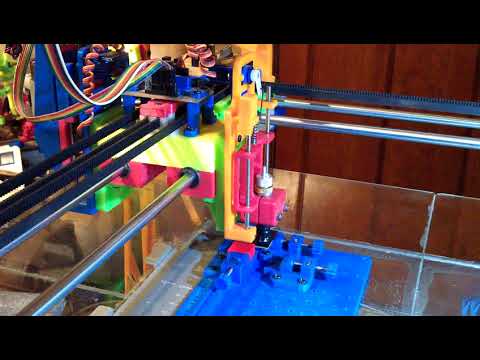
Put the Board in place and Set the Plotter Scribing.
(sorry about handshake and focus on the video, I use my old phone to do video)
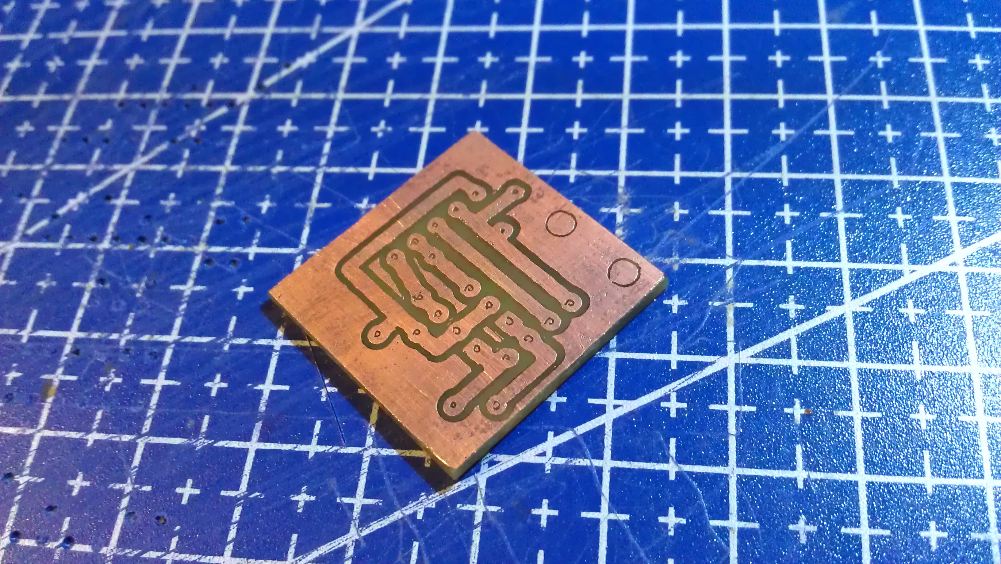
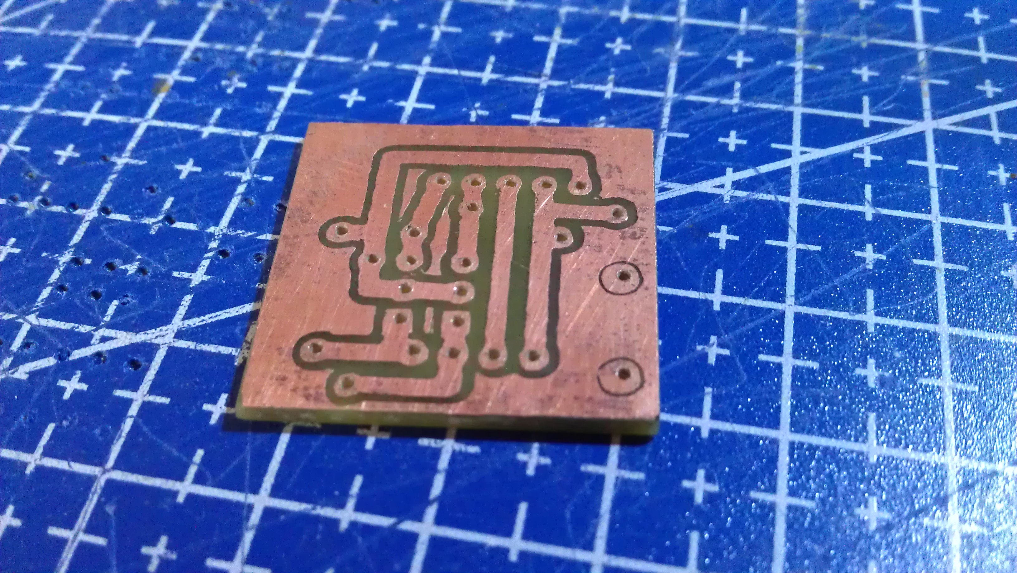
Etch the Board
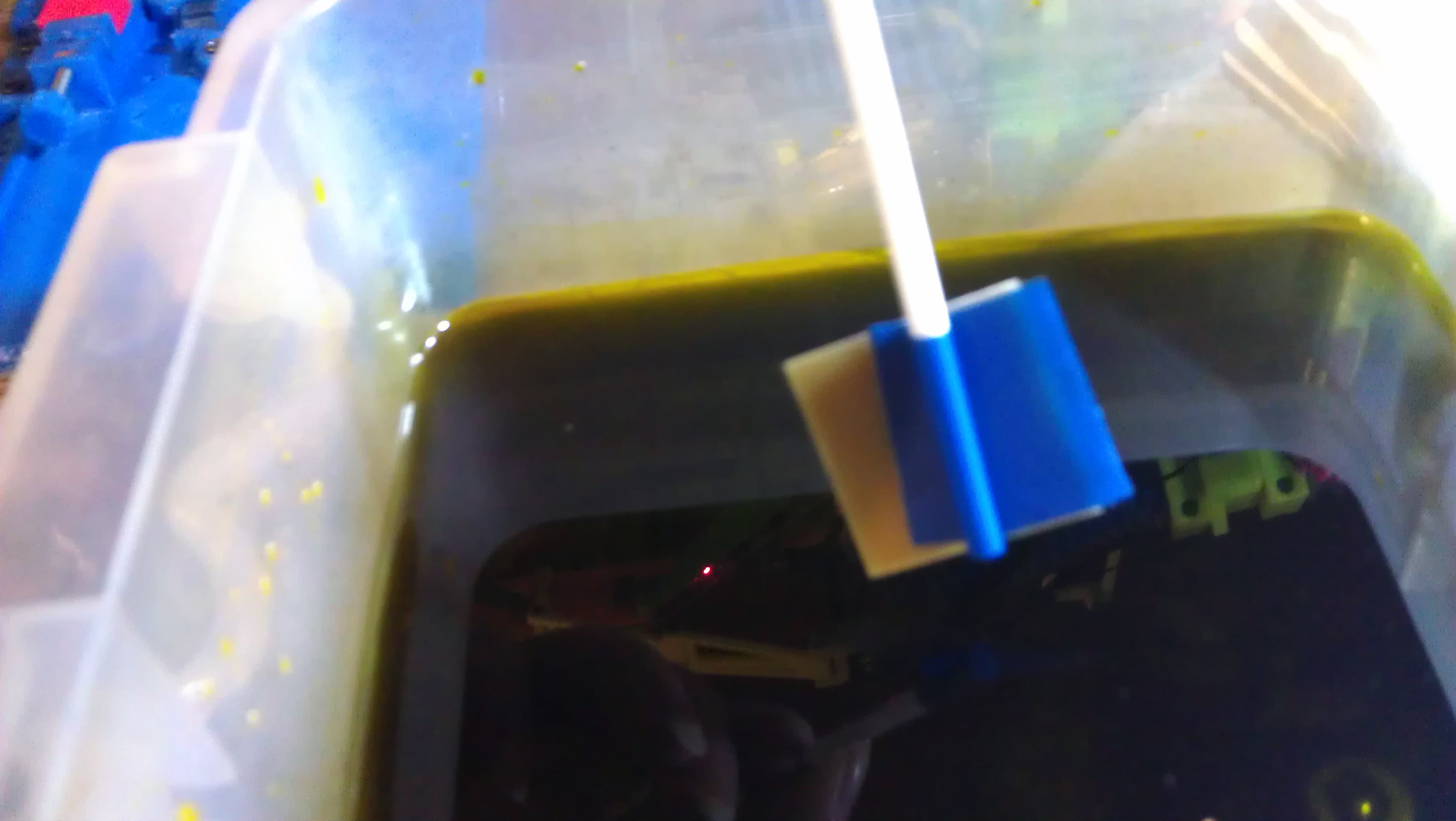
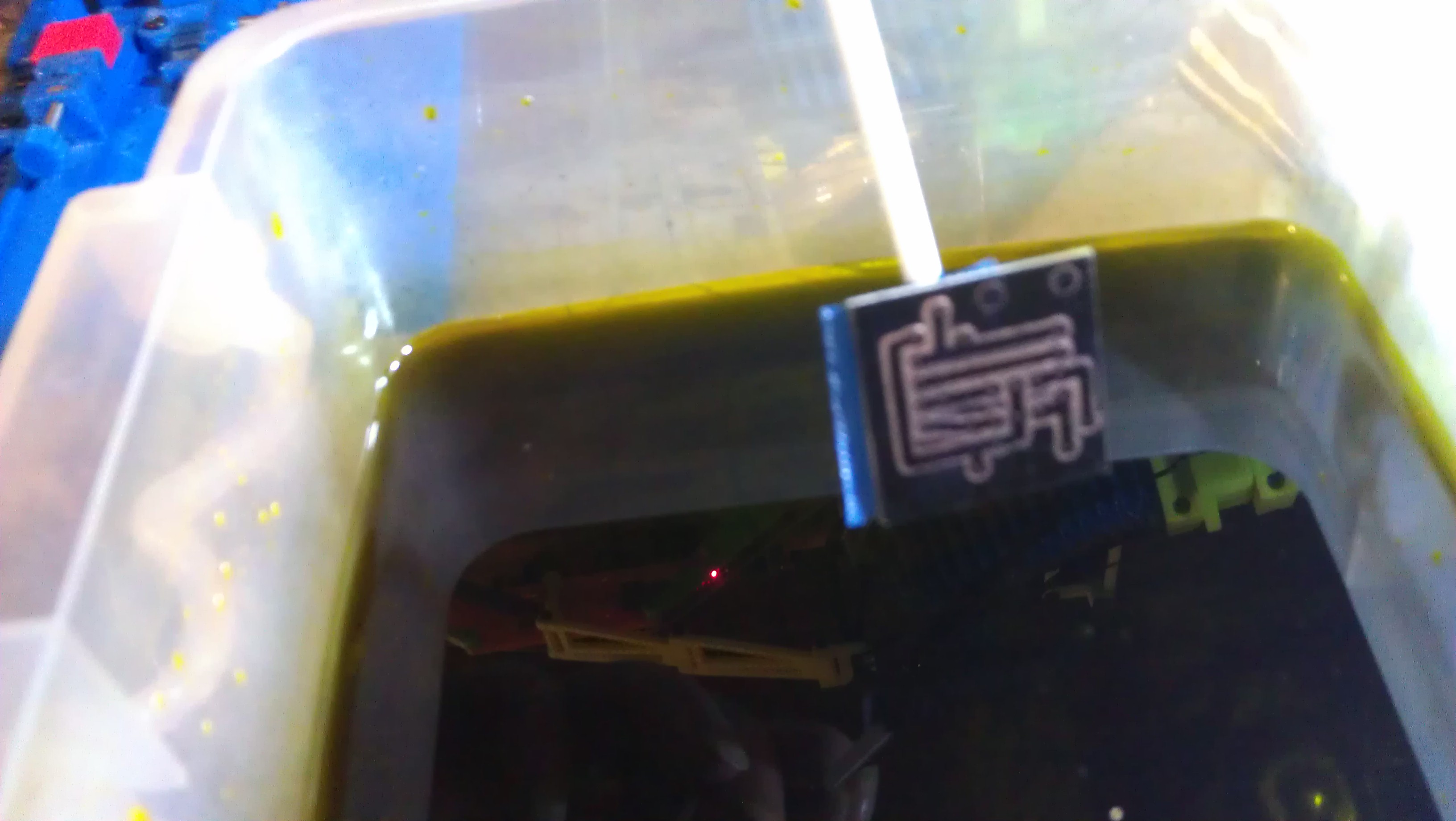
Next, dip it in Ferric Chloride for a while.
I just tape it to a plastic stick and use it like a spoon to stir up the Ferric Chloride from time to time, I feel stirring helps the etching process.
Clean the Board
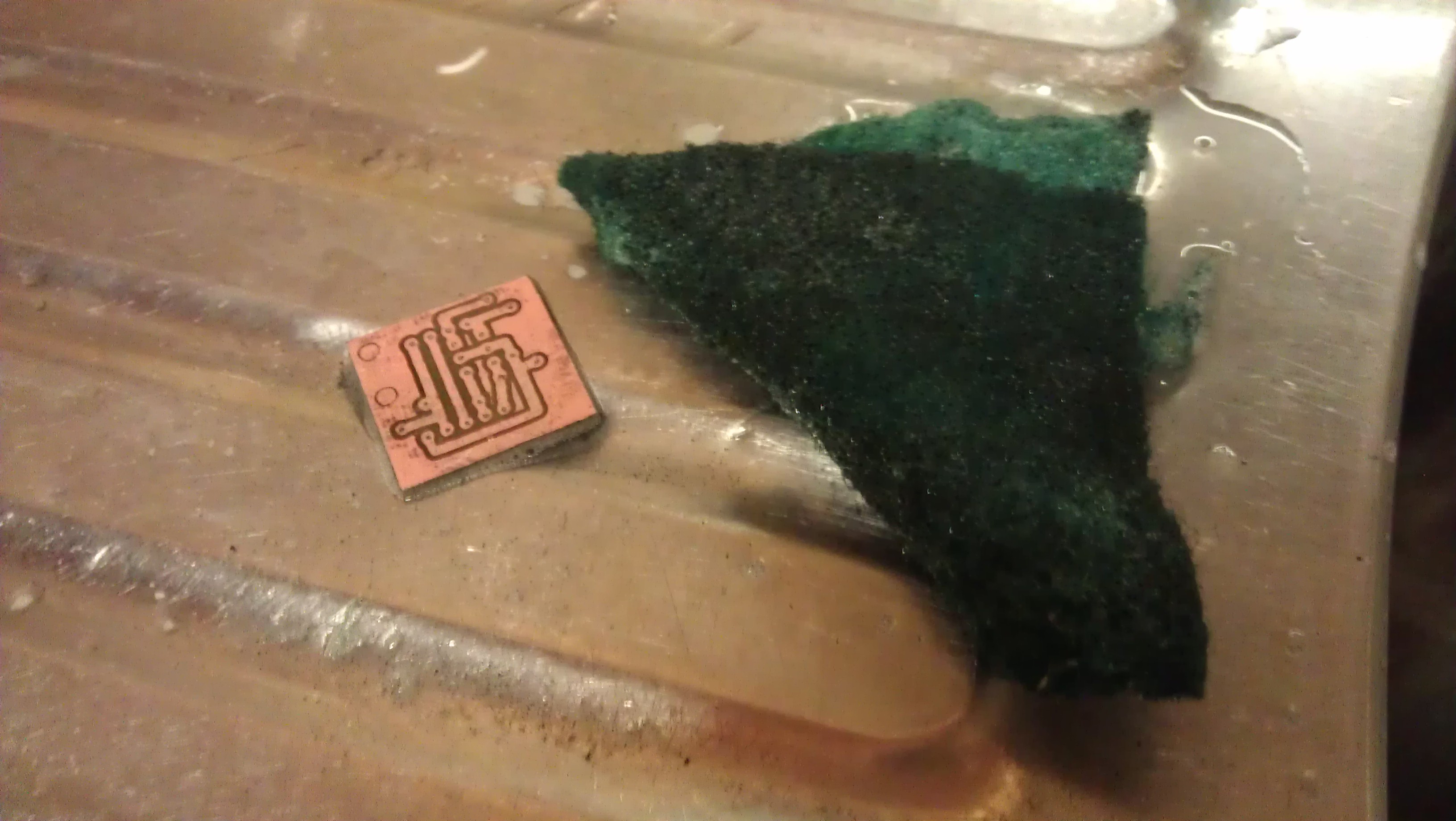
Next rinse off the Ferric Chloride and remove the ink.
I have a small brass wire brush to start the removal, and finish of with a typical pan scrubber.
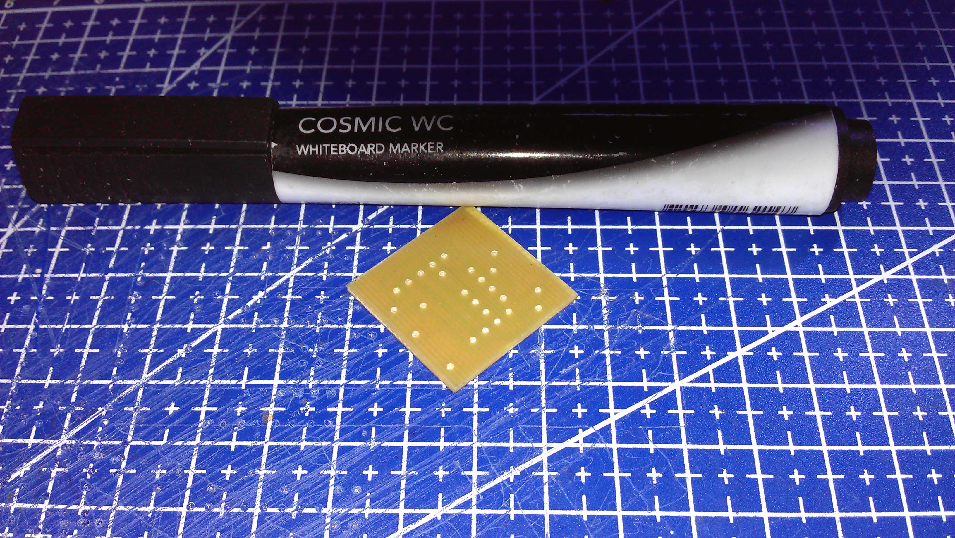
Drill the Board Step 1
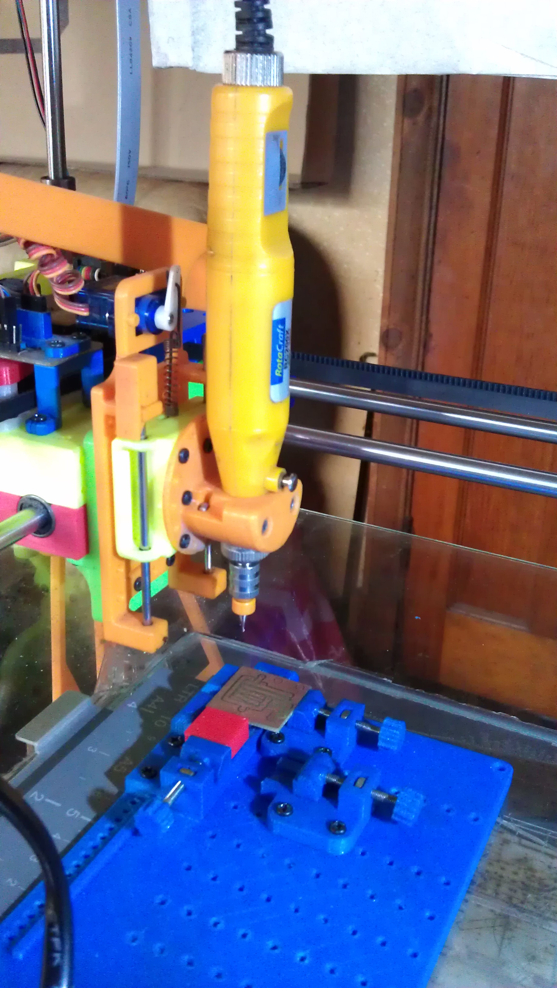
Next is to drill the board.
I drill the board from the copper side because I have a bit of wobble on my drill, and because I etch the holes, where the hole have be etched, act like a locater for the drill bit.
Also the etched holes aide in checking the alignment of the plot.
So setup my XY Plotter with a drilling tool and fit the board.
Drill the Board Step 2
I do a dry run of the plot first and make any required adjustments to the position.
(during the dry run I will turn the drill bit, because the fluting sometimes give the wrong appearance)
Drill the Board Step 3
When happy with adjustments I drill the board.
The 2 holes for the screw fixing of the board, I will enlarge my hand, using the holes drilled by the plotter as a pilot.
Draw Component Locations
The last step is to draw component locations on the top side of the board.
This could be done by hand or the plotter with a permanent marker, but I have not found a pen fine enough to do it.
So I use a laser, not an expensive one. I have one boosted to 15W and a cheep 5 volt 1 Watt one.
Although I could do it faster with the 15W one, it burns a thick line, the 1W is the one I use.
eBay search for: 1W laser It gives a fine line (not as fast but a better look)
I don't coat the top of the board with ink using a Whiteboard Marker yet I need to check the alignment of the board.
Laser Step 1
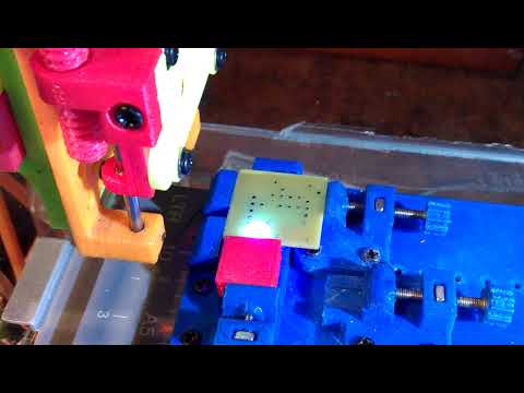
Because I have now turned the Board top face up.
This is where I use the ???_drill (top).tgc file. to align my XY Plotter with the board.
So I set up my Plotter with the laser and place the Board in the jig.
Run the ???_drill (top).tgc file to check alignment, adjust as required.
I just check a few holes, because the board is opaque (semi-transparent) the laser does nothing to the board.
The focal point of the laser did not show in the video, I tried putting the safety glasses in front of the camera but it didn't help.
I hope you understand what I was trying to show.
Laser Step 2
Once I happy that all is aligned correctly, it's time to coat the top of the board with ink using a Whiteboard Marker. (chisel tip best)
(don't mix up your pens)
Laser Step 3
Place the board in the jig and etch the component locations with the laser.
(I'm sorry I make these videos with my old phone and sometimes it does not focus well close up)
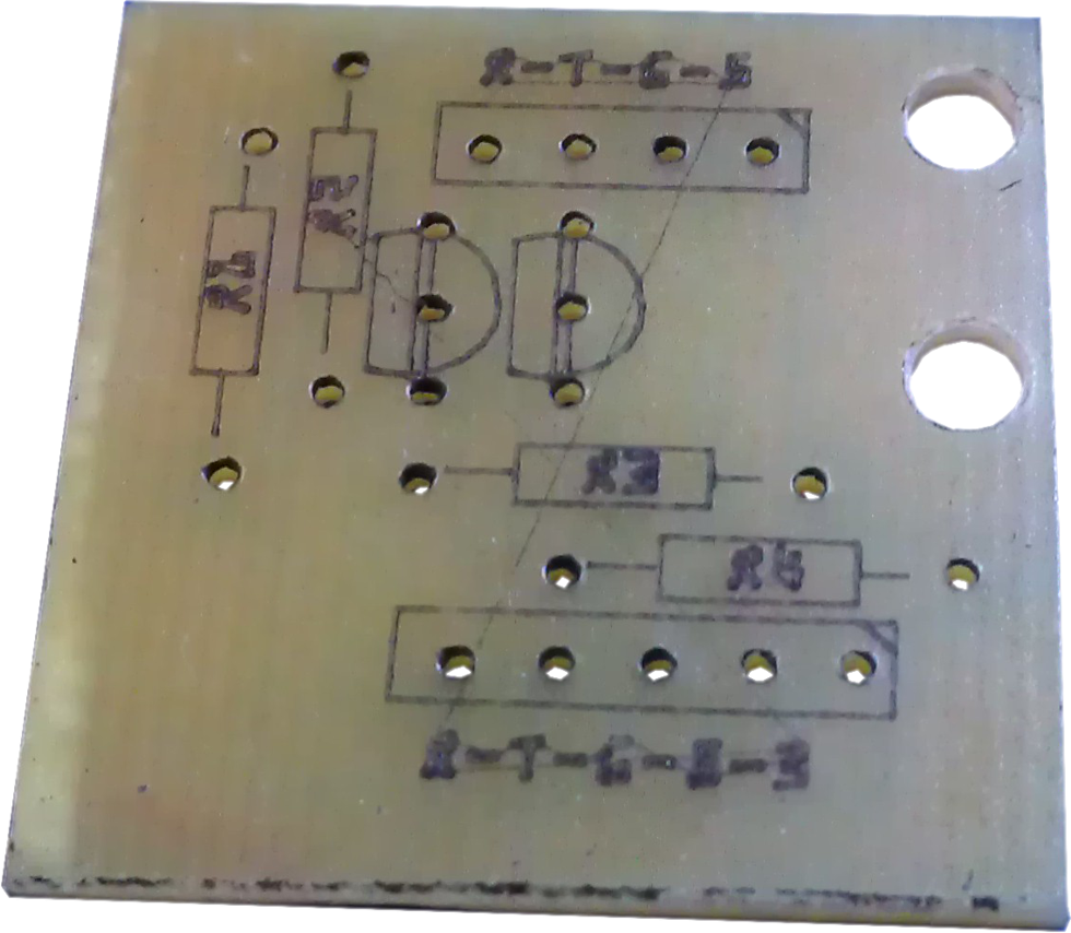
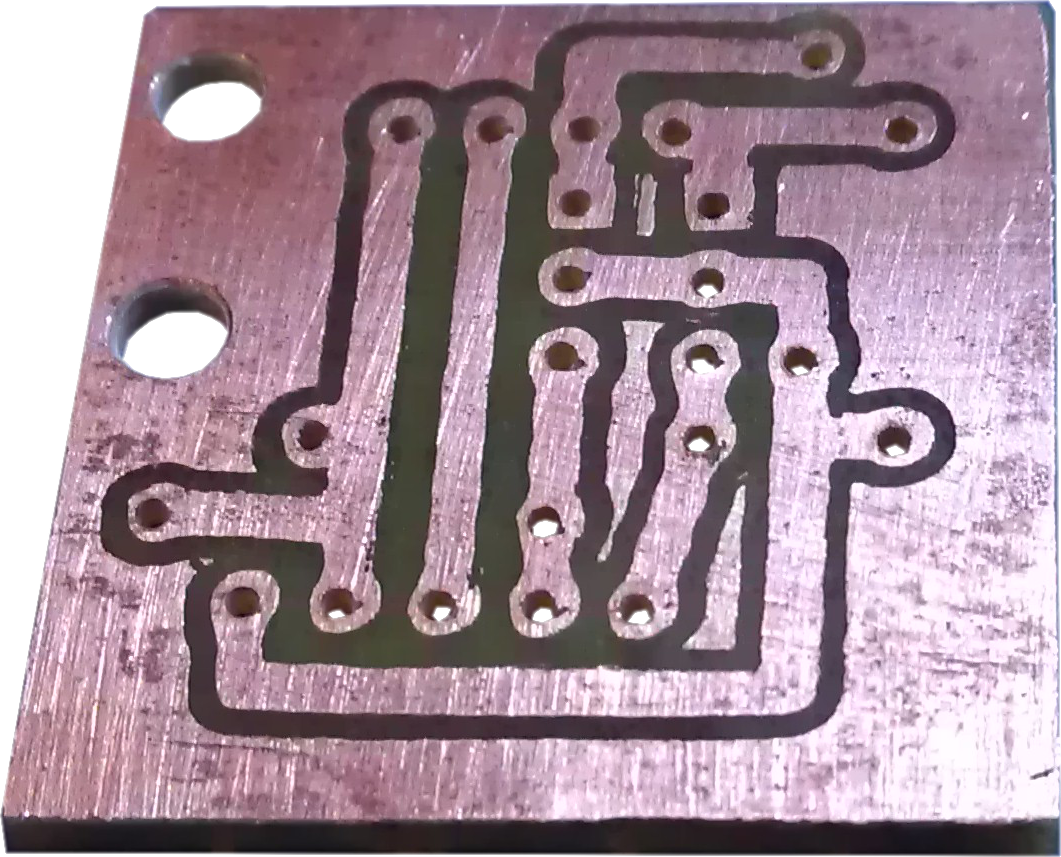
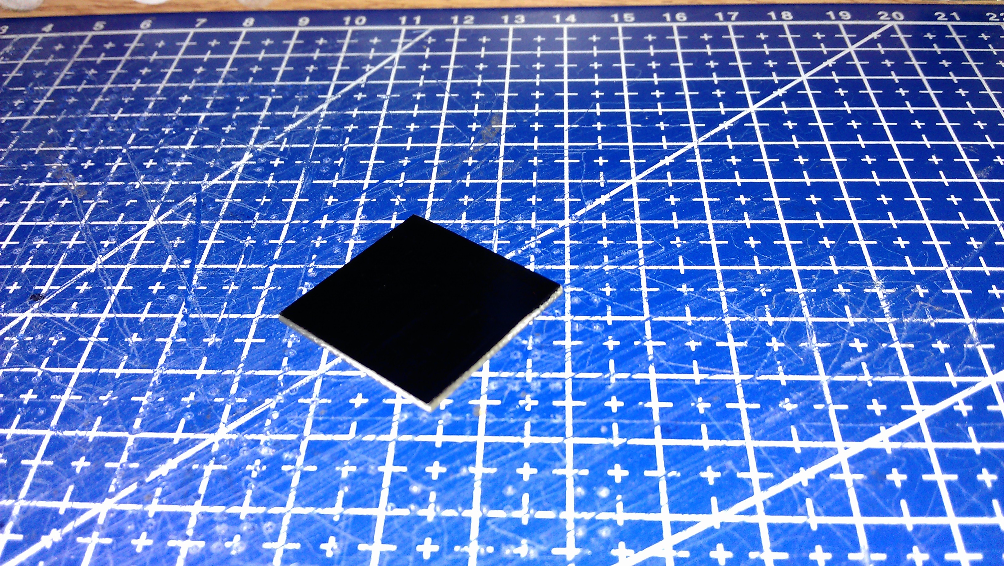
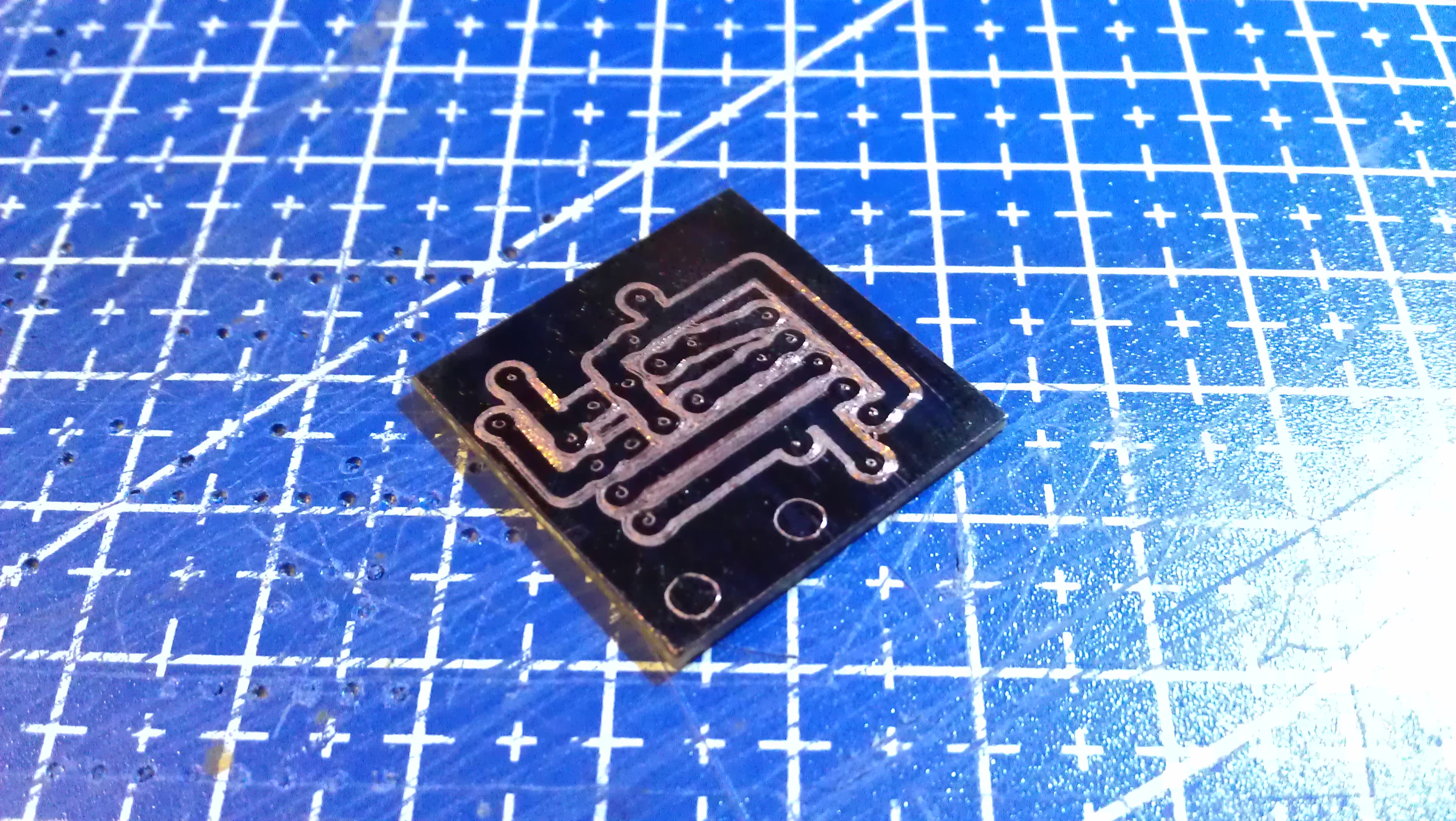
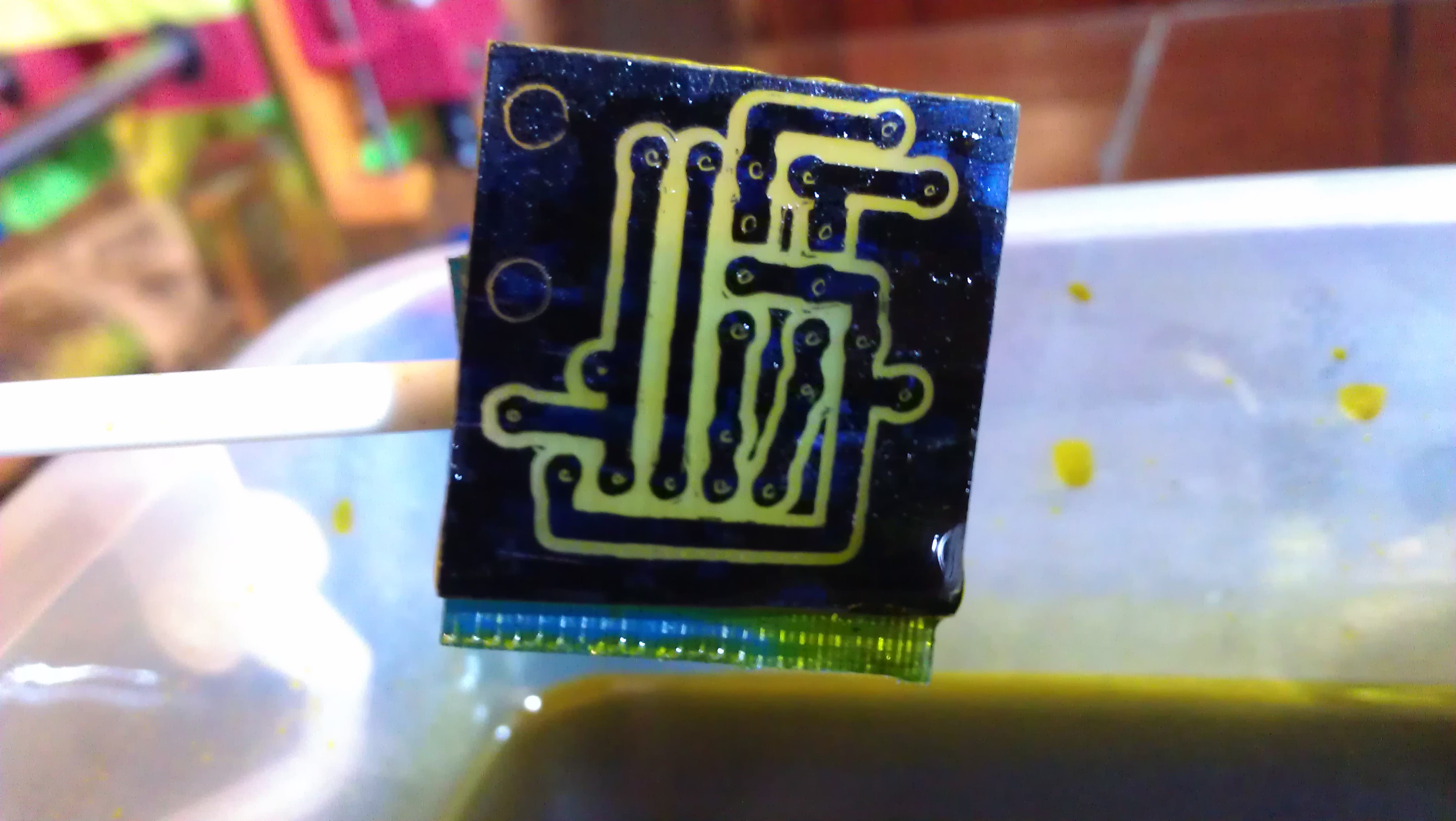
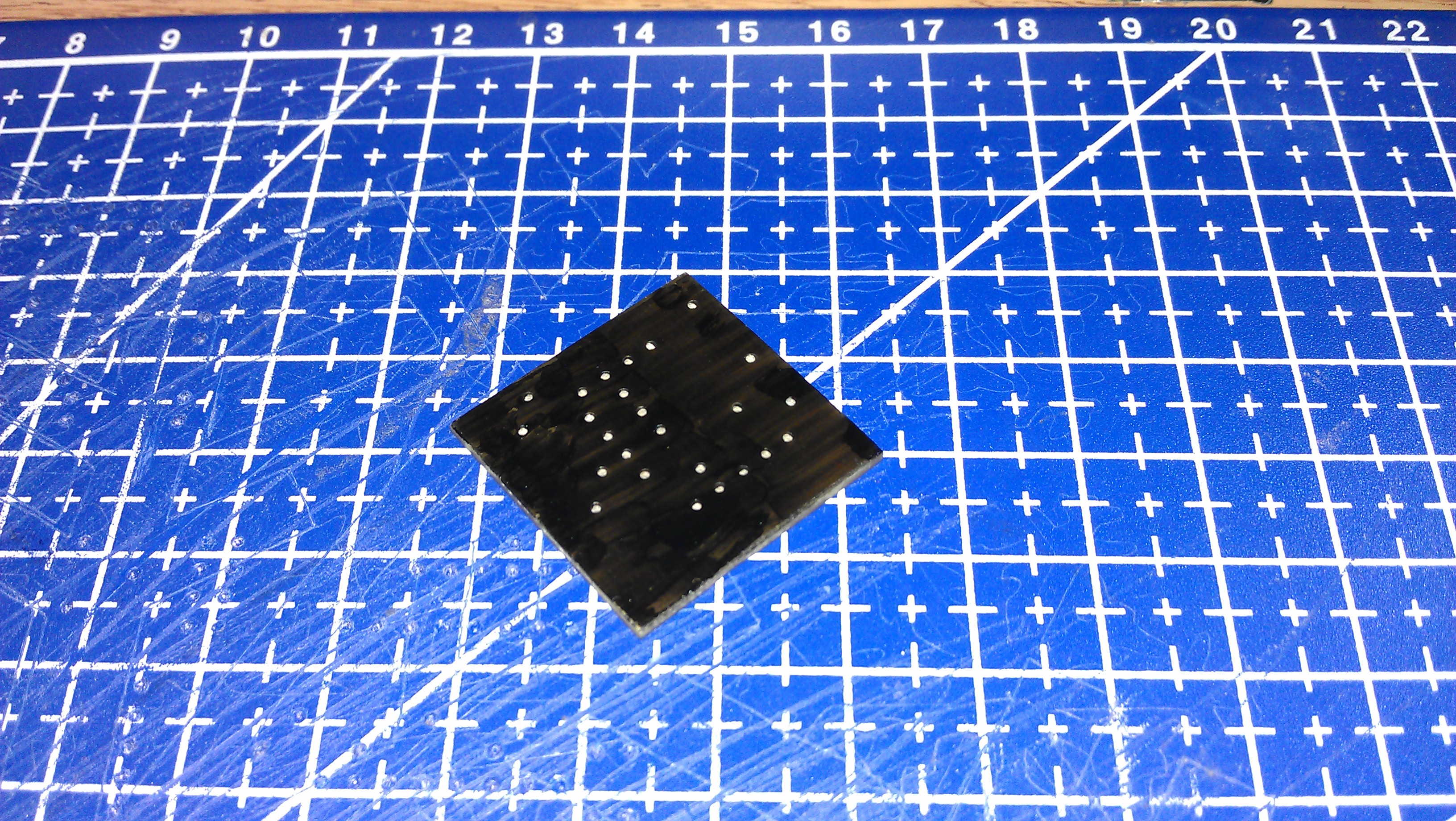
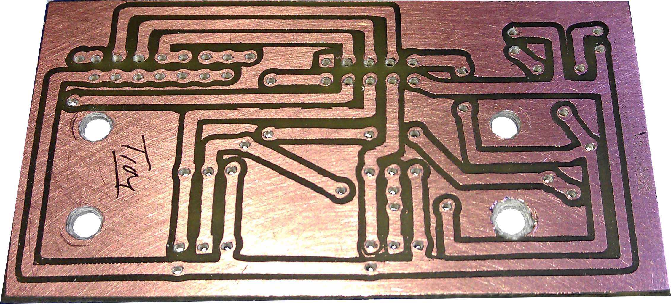
The Finished Board
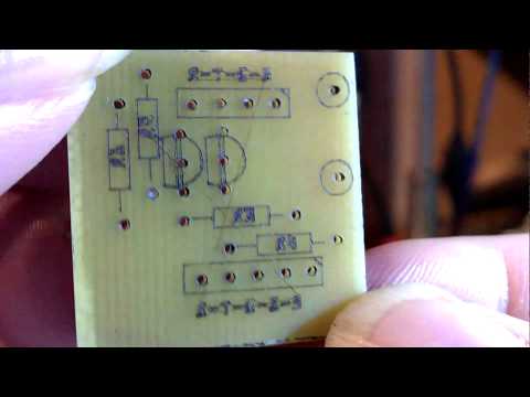
The finished Board:
Hope you find something in the methods I use of help.
The Plotter I use is one I have designed and built my self, and wrote the Firmware and Software also.
I'm currently in the process of writing a blog on how I made the plotter here: Tim's XY Plotter I may convert it to an instructable here when I get around to finish the blog.
Some Other Boards
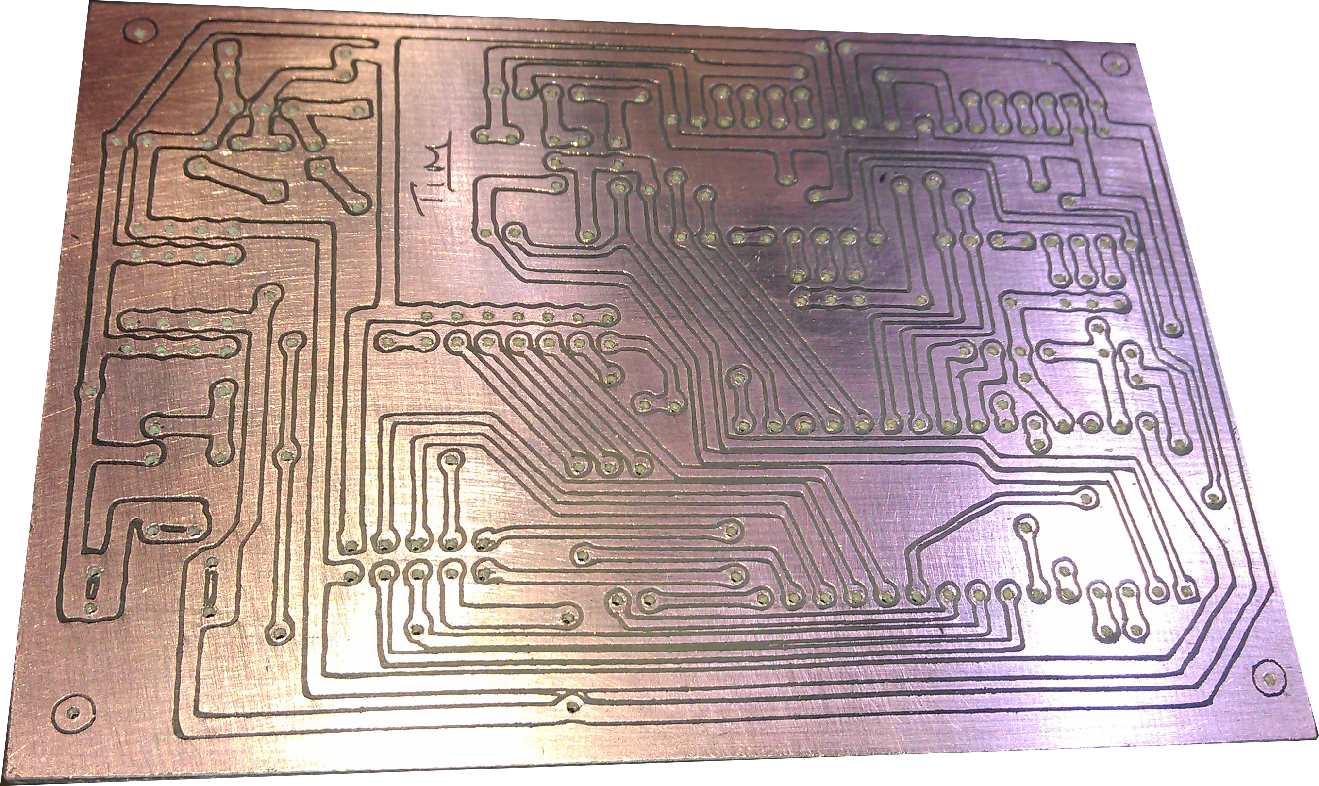 Bottom.png)
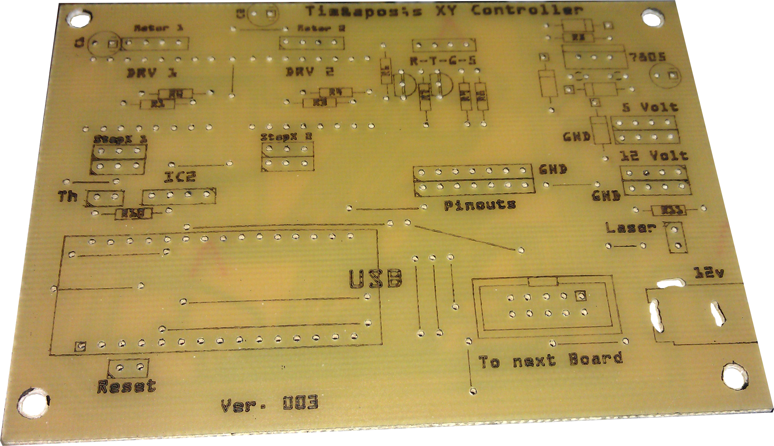 Top.png)
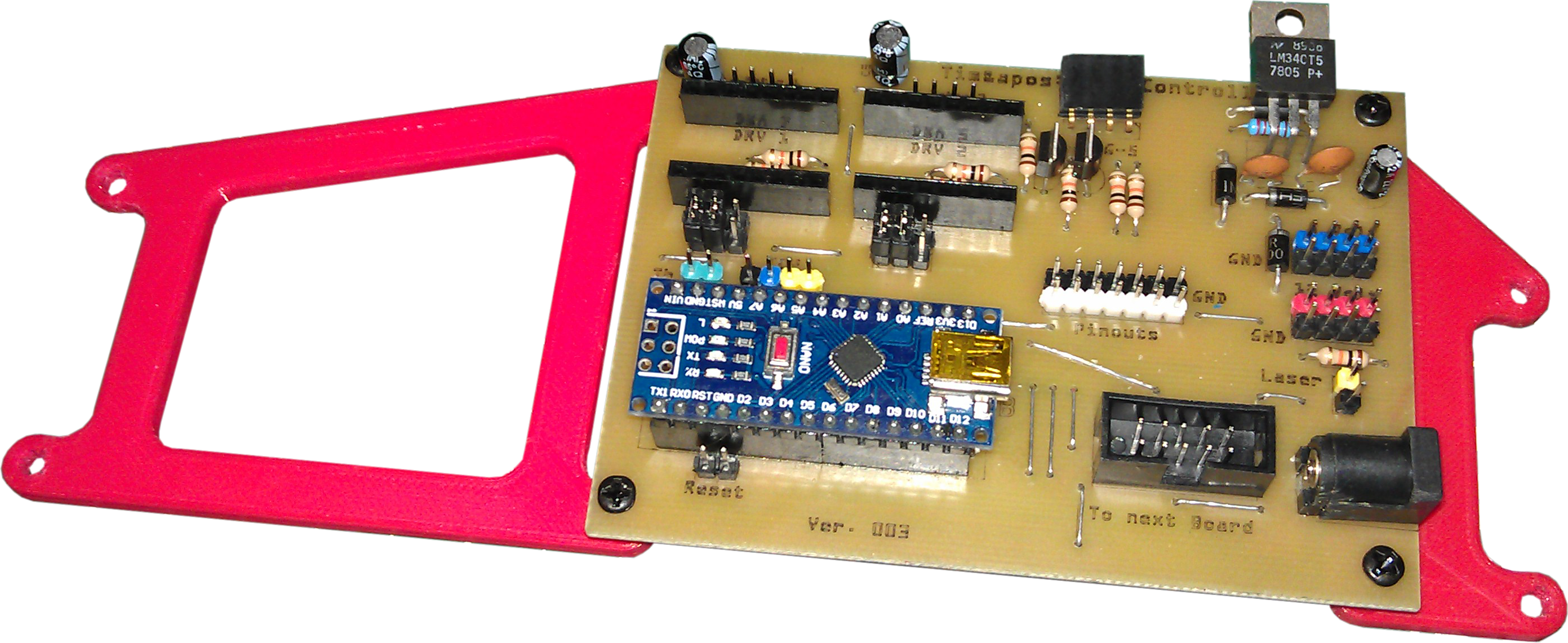 with Components.png)
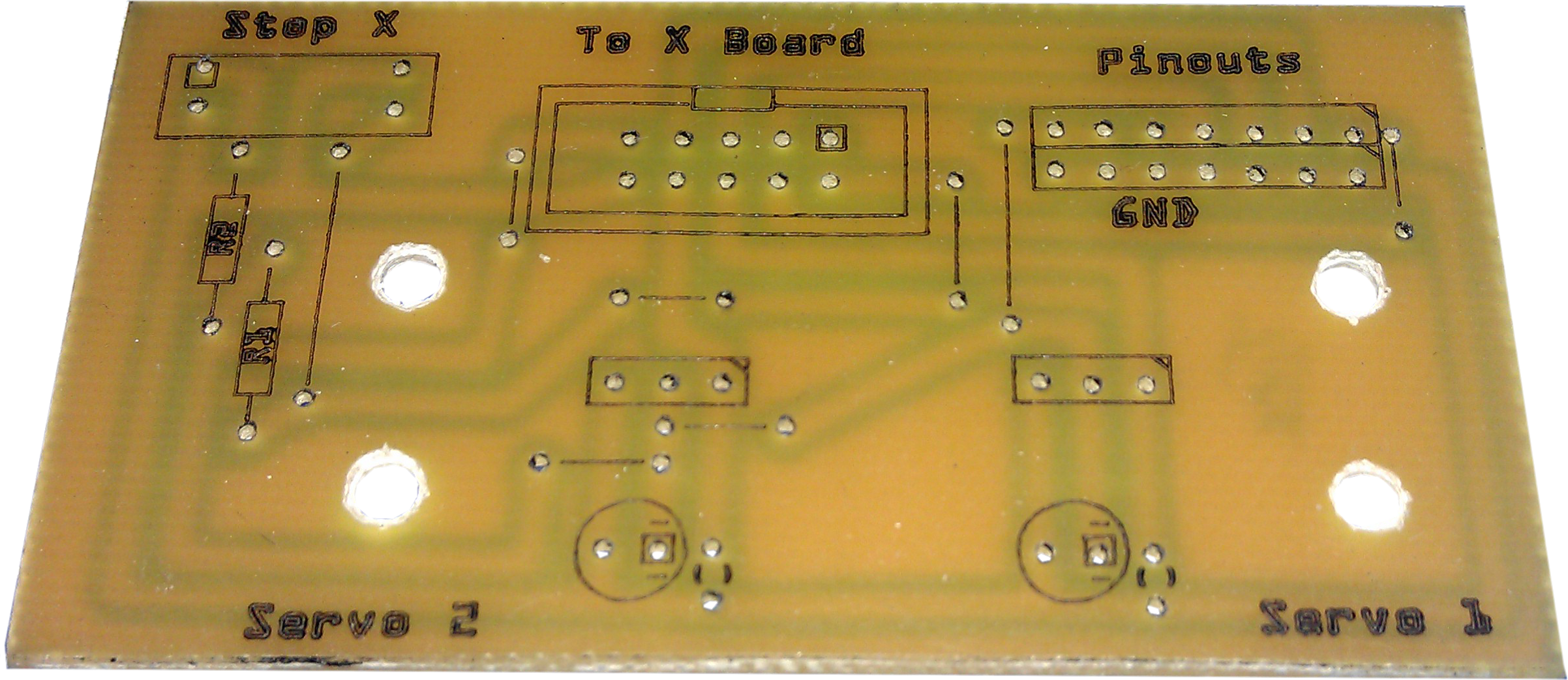
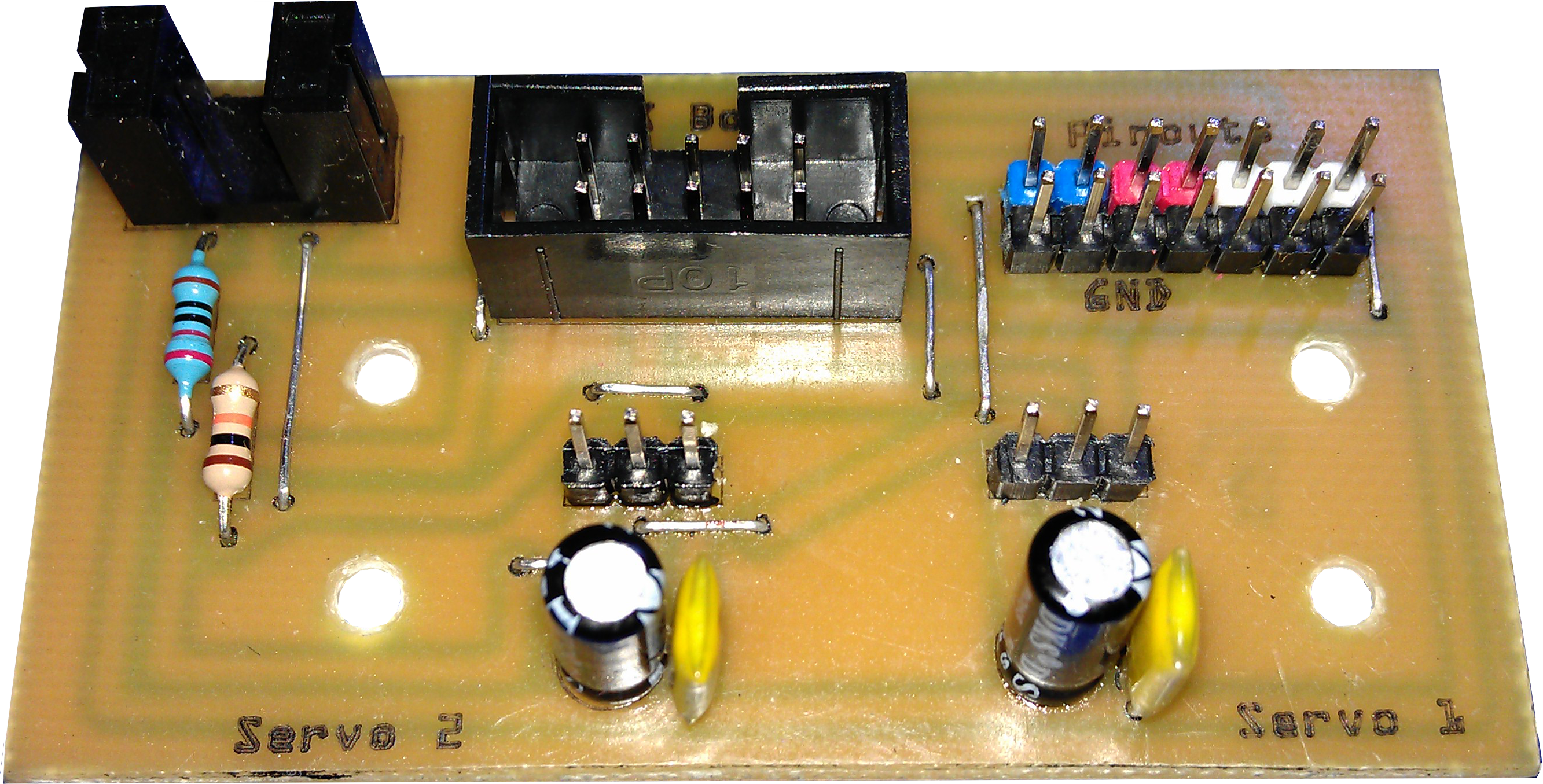
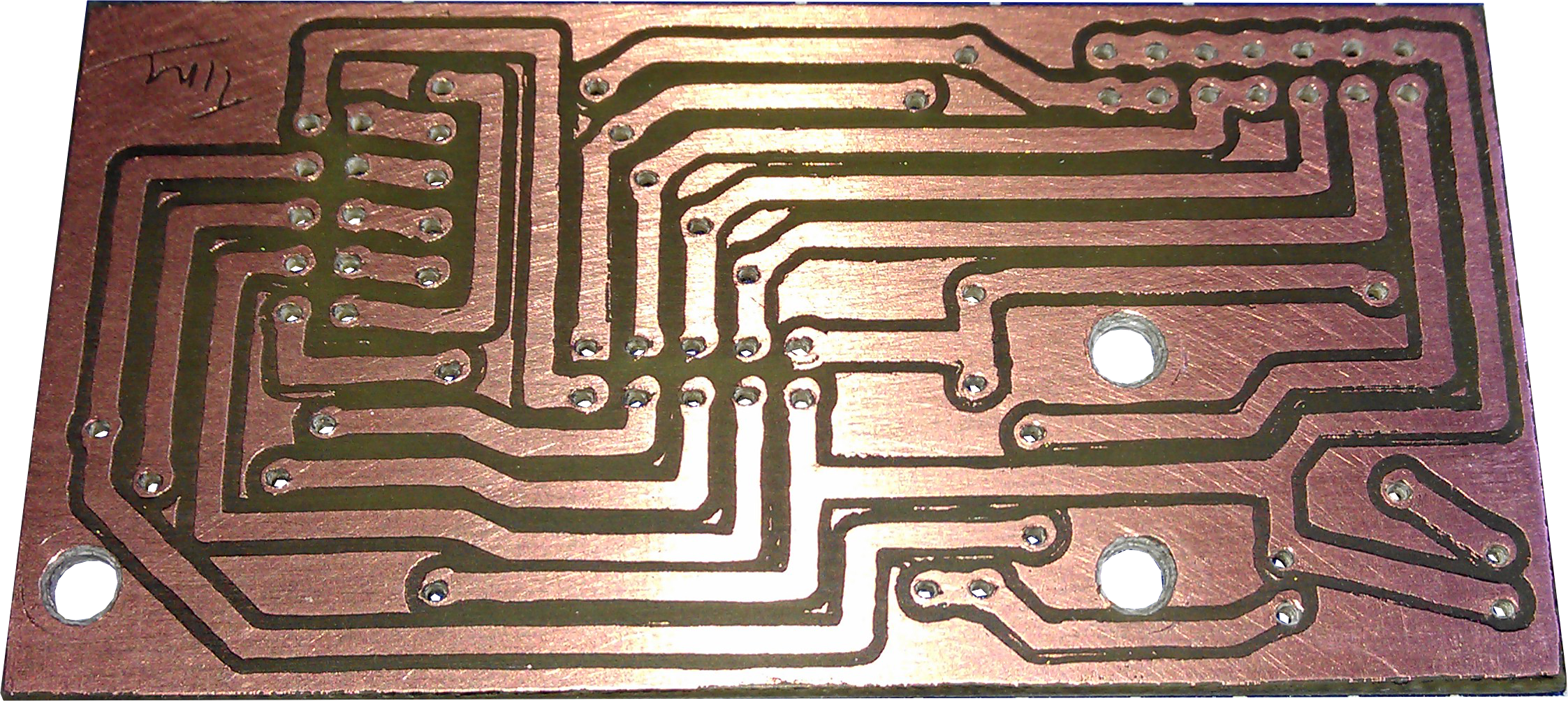
Here are a few other boards I have made using this Process.