Testing Chinese AD/DA Data Acquisition Module
by GandaU in Circuits > Electronics
1514 Views, 7 Favorites, 0 Comments
Testing Chinese AD/DA Data Acquisition Module
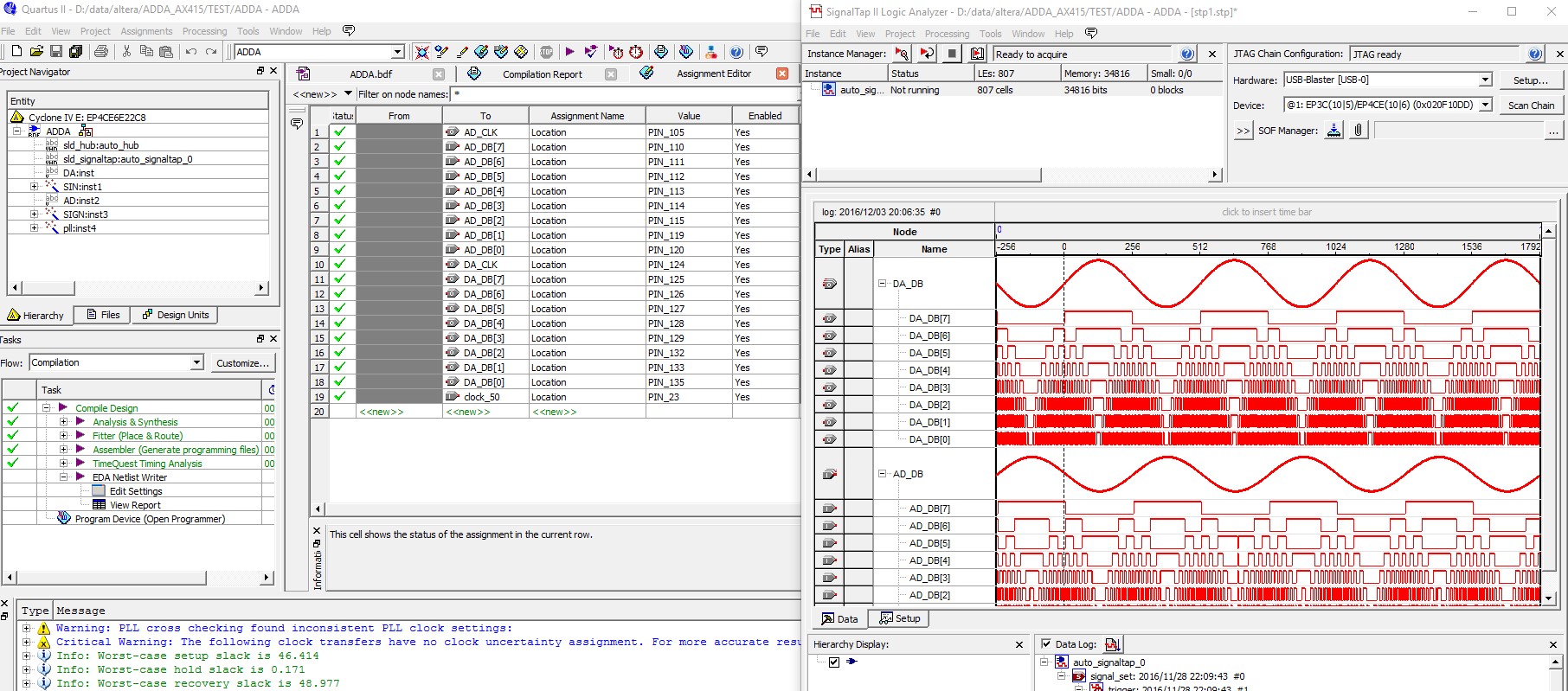
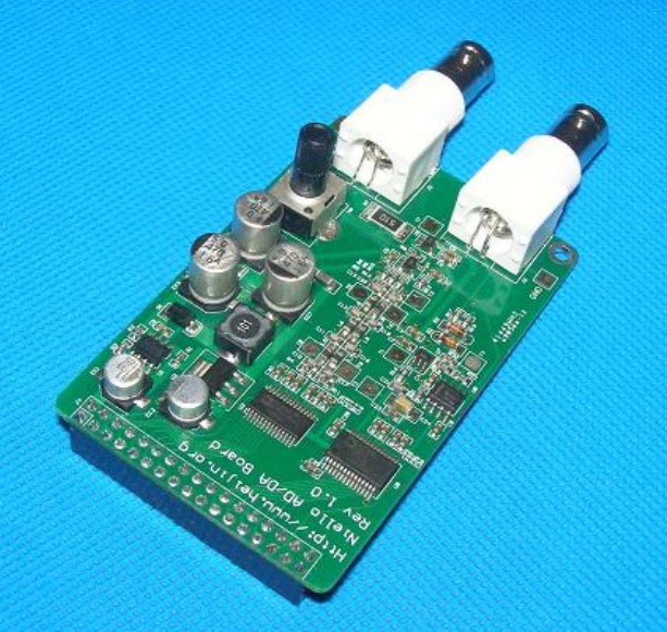
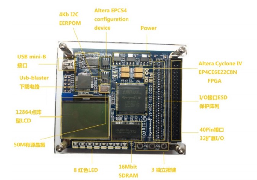
Recently, I bought cheap Altera board and a data acquisition board A/D D/A from Ali express module from two different stores. These boards are cheap yet not pin compatible to each other. They came with samples and manuals. Reading this manual in Chinese caused me headache :). Yet with the help of google translate, I managed to understand and connect them both with jumper manually.
So here I share them how I play them.
Connect Them Using Jumper Cables
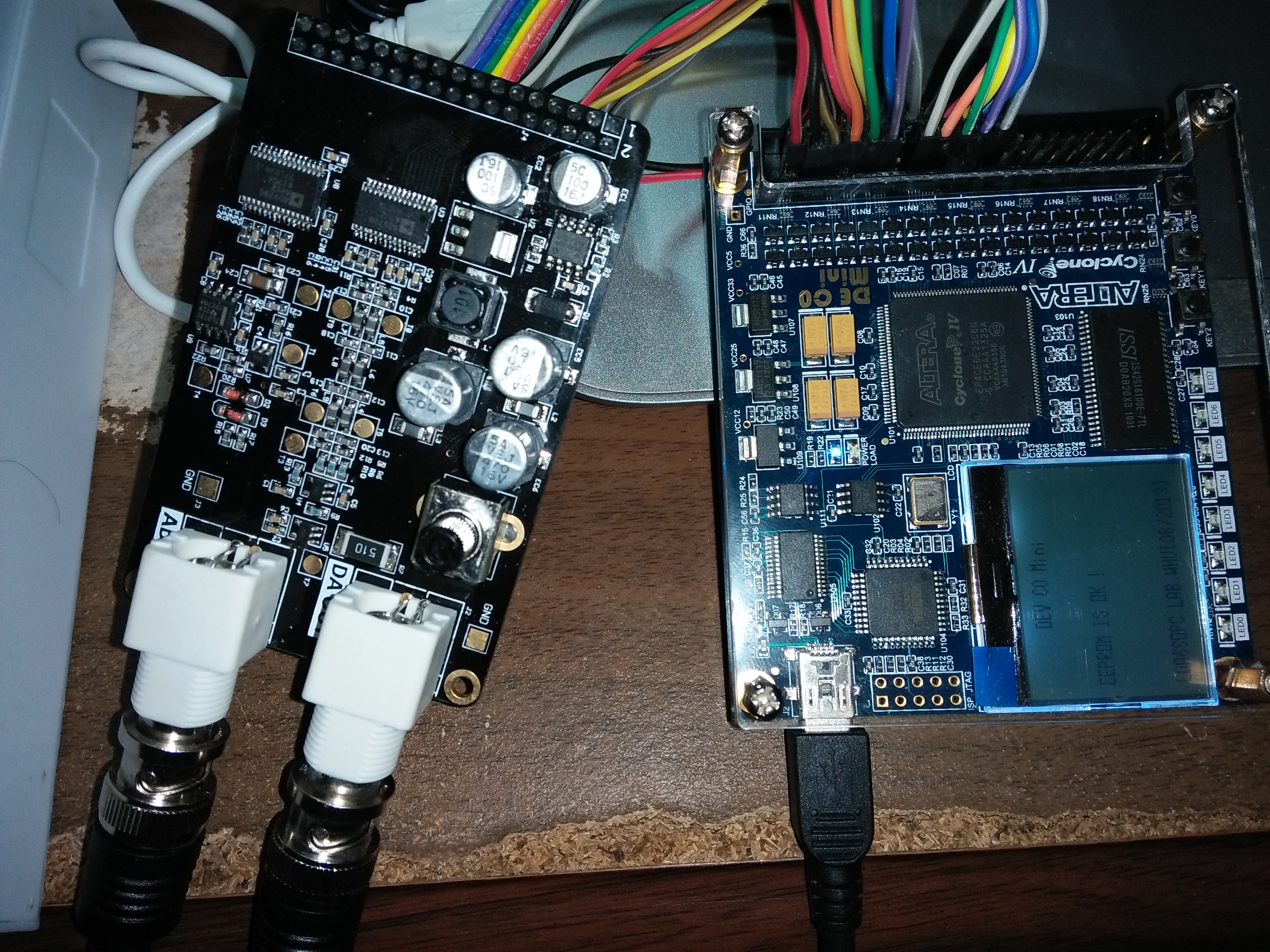
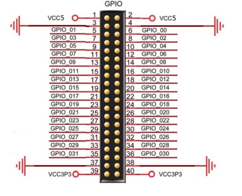
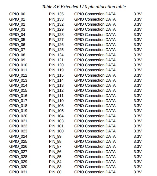
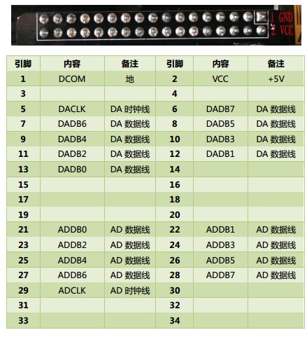
Ideally this data acquisition board can be plugged directly to the FPGA core board if the pins are matched. We can change any data pin assignment using Altera Quartus-II software but unfortunately the power and ground pins requires 5 volts instead of 3 volts, so this forces me to jumper them manually.
Since there are A/D and D/A chips inside the acquisition board module, we can connect D/A output to loop back to A/D input. So it will show output A/D and input D/A later.
Also, there is a potentiometer to adjust the amplification of signal coming to A/D. this can be adjusted so it will show good signal sample in Signal TAP later.
Reconfigure Sample Program Pin Planner
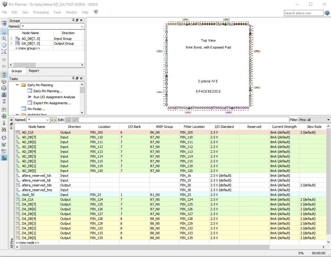
The sample project from the A/D D/A Data acquisition module need to be modified according how we connect them to the main FPGA board. This saves time rather than if we re make them from scratch. I use Quartus II version 14 web edition which can be downloaded from here.
From the Quartus-II software, click assignment -> Pin Planner and change pin you connected them both.
Recompile Code Example
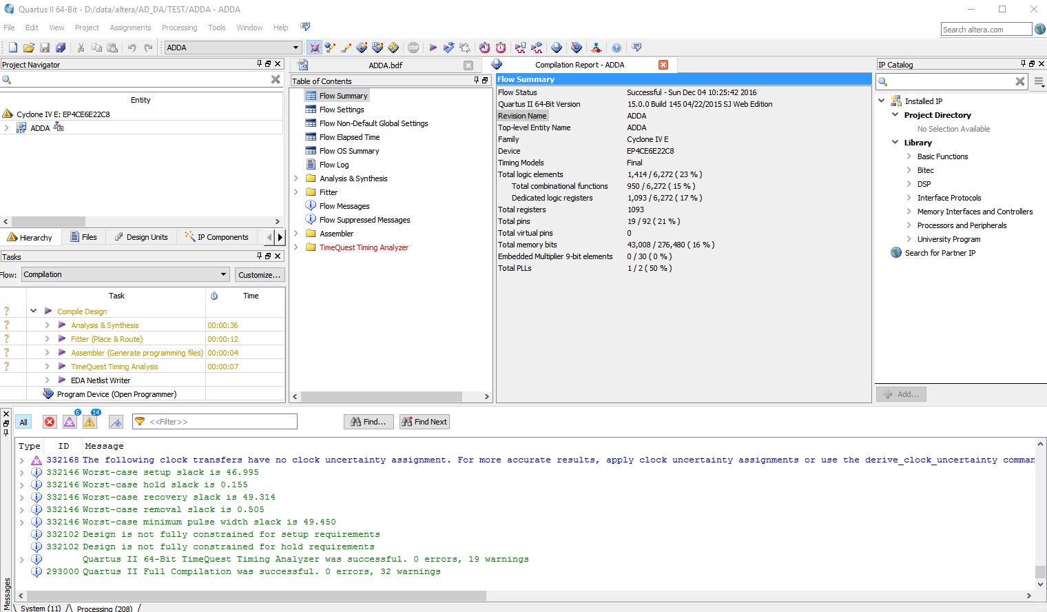
After modifying the pin planner according to your need then you compile the example project.
In case you are interested, you can download Example from here.
Re Run the Signal Tap
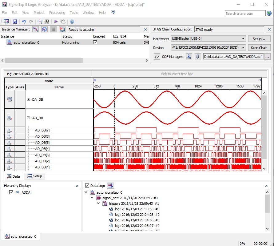
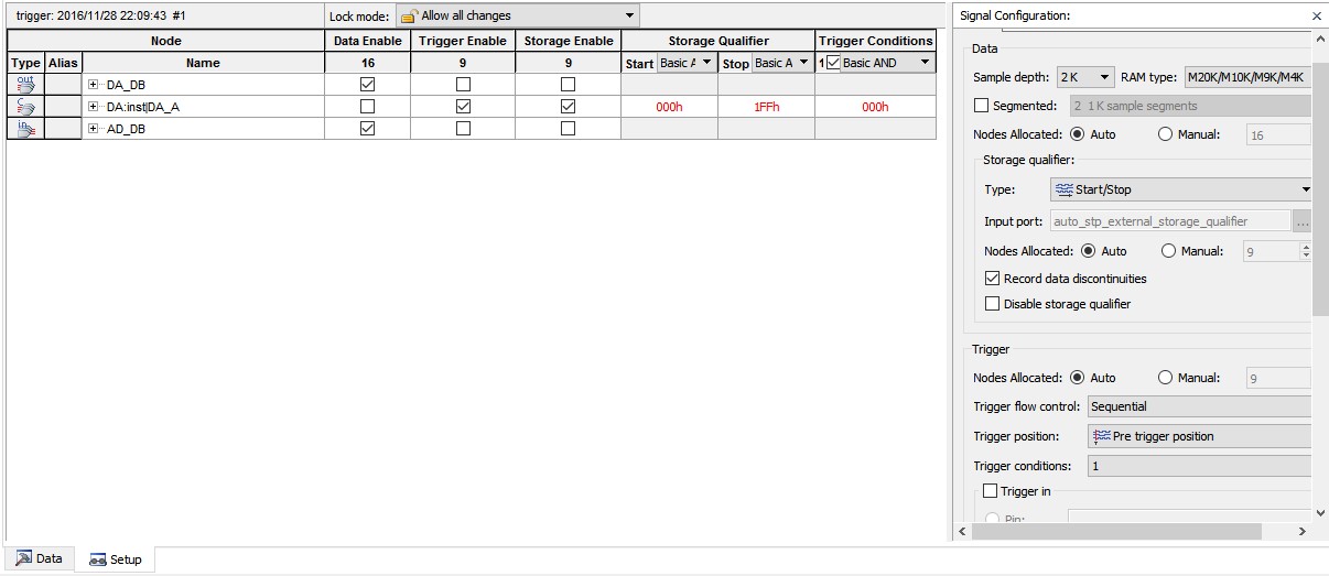
From Altera Quartus II click Tool -> Signal Tap II logic analyzer.
Re program the SOF file using Program Button on the SOF Manager on the right corner. And click run button.
I encountered triggering problem regarding using this toolbox but I managed to setup the trigger using storage qualifier and trigger condition that trigger start data tapping when DA =000h until buffer full (has depth of 1K samples), only valid if data is from 000h to 0x1FF.
That's all, thanks for the reading.