Simple Tips for an Effective PCB Design Check (EAGLE Software)
by JayconSystems in Circuits > Electronics
2746 Views, 16 Favorites, 0 Comments
Simple Tips for an Effective PCB Design Check (EAGLE Software)
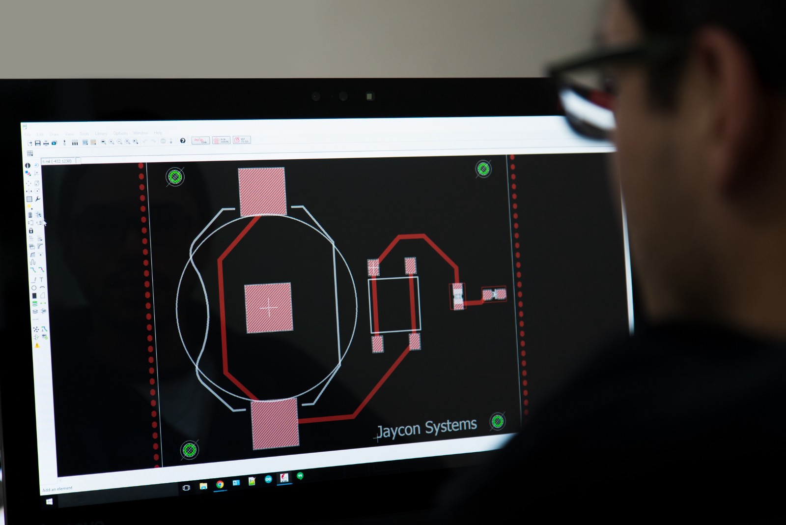
After many hard-working hours, you finally have your PCB design completed and ready to send it to a circuit board manufacturing company (aka Jaycon Systems). But how can you ensure that the PCB you just designed is going to meet your expectations when manufactured?
In this article, we will give you some simple but effective tips on how you can make your PCB look and work just the way you expect when sending it to a manufacturer.
If you are reading this article, you most likely are already familiar with the Eagle CAD software to design PCBs. In case you are not, there are hundreds of tutorials out there that can teach you how to use Eagle. Today we won’t be focusing on how to design PCBs, but rather on what to do once the design is complete.
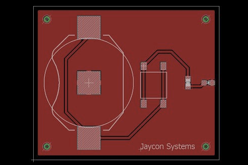
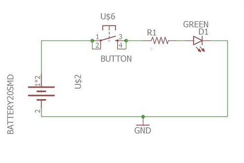
Let’s take the following circuit shown above (Fig.1 — PCB Layout) as an example. This is a very simple circuit that turns a LED on whenever the push button is held down (Fig.2 — PCB Schematic).
Tip 1: Check for Shorts
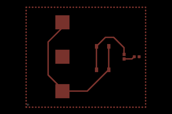
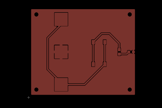
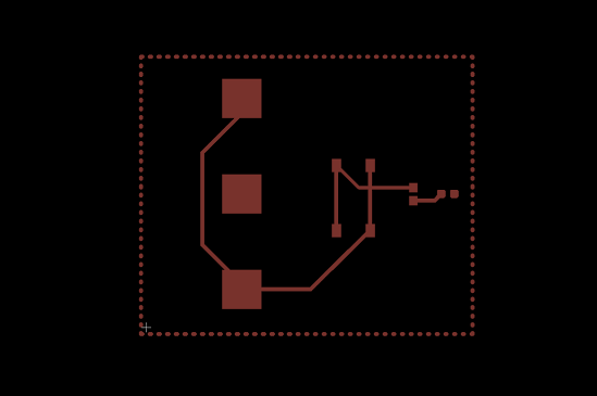
One of the first things you can check for is shorts. These are caused by overlapping two or more traces on the same layer. Simply clear all layers in Layer Settings except for the top layer.
Fig.3 — Top Layer: This is a very easy way to visually inspect the board to make sure the traces are good.
You can even apply Ratsnest to have a better view of your layout.
Fig.4 — Top Layer with Ratsnest
Now let's see how a short would look like:
Fig.5 — PCB with a Short: You can see it is very easy to spot a short with this technique.
Tip 2: Click on All Components to Ensure Nets Are Connected
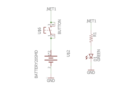
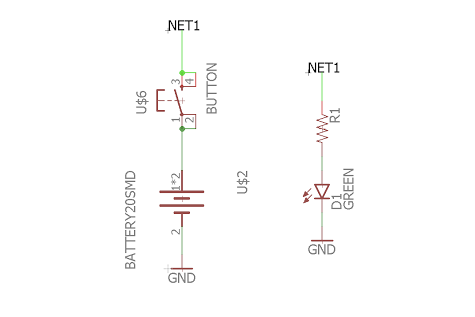
The second recommendation we have is clicking and moving around the components on the schematic to make sure the nets are connected. Sometimes it may look like a net is connecting a component, but this is not always the case. If the nets attached to the component move as you move the component around, then the connection is good. Otherwise, delete the net and draw it again. In some cases the net is not attached to the component but rather connected using the Name feature — like in the example below:
Fig.6 — Virtually Connected Nets
In this case, you can either check that the name of the net (in this example NET1) is the same wherever it is used, or you can use the Show function to highlight the net everywhere in the schematic — as shown below:
Fig.7 — Nets with Same Name Highlighted
Tip 3: Use ViewPlot to View Your Gerber Files
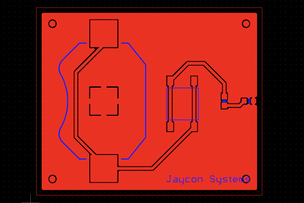
Another way you check your PCB design is by using a software called ViewPlot — it can be downloaded directly from their official website. ViewPlot is a free CAD software viewer that allows to you to see the Gerber files of your design. To use it, simply open ViewPlot and drag and drop the Gerber file you want to view. For example, let’s view the top and silkscreen layers of our circuit:
Fig.8 — ViewPlot
If we compare figures 1 and 8, we can see that everything looks the same except for the text “Jaycon Systems.” In ViewPlot it appears shifted to the right and it interferes with a via. Even though it may look fine in Eagle, in real life the circuit will look the way it shows in ViewPlot. This is mostly because this is the Gerber file — not the Eagle file — which is what PCB manufacturing companies use. In order to fix this, you have to go back to Eagle, move the text away from the via, and generate a new Gerber File.
These are three simple steps you can take to check your PCB design without having to go through Eagle’s DRC, which sometimes can be aggravatingly intricate.
Always review your design before sending it out for manufacturing. Following these simple steps doesn’t take long at all. A simple mistake like a disconnected net may cost a few hundred bucks to thousands of dollars when you are mass producing your boards. And don’t forget — if you need help with PCB design and/or manufacturing, get in touch with Jaycon Systems today.
Originally published on Medium