Sensor Fusion Introduction
by SensorFusion in Circuits > Gadgets
2788 Views, 8 Favorites, 0 Comments
Sensor Fusion Introduction
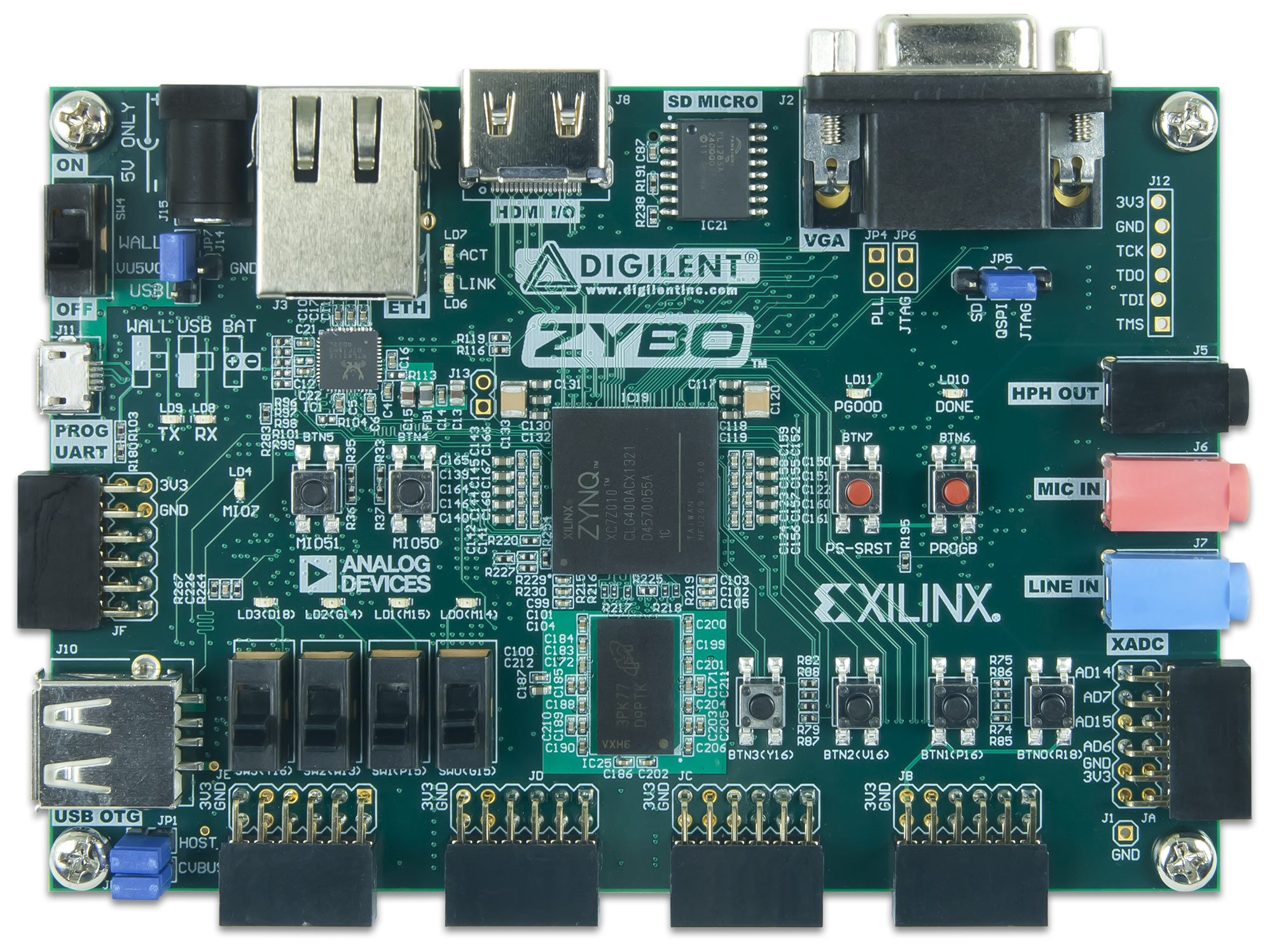
Hello, In this tutorial we will be walking through the process to create a device that uses GPS coordinates and acceleration data to plot a more accurate path than logging pure GPS data points alone can provide. To do this we will work to implement a "Kalman Filter", and apply it to gps data. The more accurate position generated by applying the filter to points gathered by the GPS module can then be written to a csv file on a micro SD card, and then used with external plotting programs to see the course recorded. While we have not reached a final solution due to time constraints, all of the subsystems are operational and require only a few additions to work correctly. The source code for these subsystems, and a main driver, are included towards the end of this report.
Required Items:
Digilent Zybo board
BNO055 IMU
Adafruit breakout board for MTK3339 GPS Transceiver
Bread board & Jumper wires (or any other functional equivalent)
Micro SD card
Required software:
Vivado design suite
Vivado HLS
FreeRTOS kernel - download here.
Hardware Setup: the BNO055 IMU
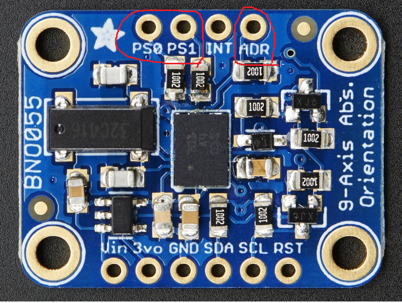
Before delving into the software, we need to ensure that all the physical components are connected properly. There are a number of tricky connections that need to be made, particularly on the IMU, to ensure that it uses I2C correctly.
Pins PS0 and PS1 (pins 5 and 6) need to be held low to use standard I2C communication, and ADR (pin 17) must be held low to use the correct I2C address.
Hardware Setup: the Zybo Board
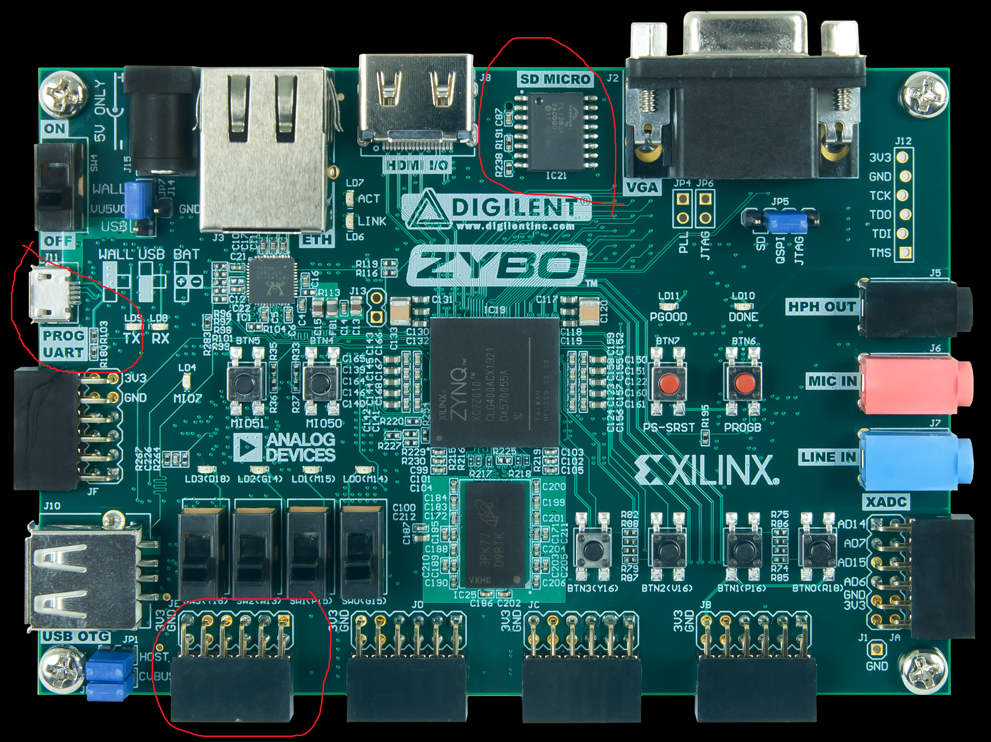

The Zybo board has 5 PMOD blocks, of which we will be using one to establish UART communication with the GPS, and I2C communication with the IMU. Also don't forget to put a micro SD card that is empty or that you don't mind losing everything on into the micro SD card slot (It's on the underside of the board), and of course the USB connection to a computer to program the board.
The first figure shows where on the board each of these connections is. The the second is a more detailed guide for connecting the I2C and GPS to the correct PMOD pins. SCA and SCL are pins on the IMU, RX and TX are pins on the GPS. Don't forget to "cross" the TX and RX pins between the GPS transceiver the Zybo board! The red pins are Vout and the blue are GND.
Creating a Vivado Block Design
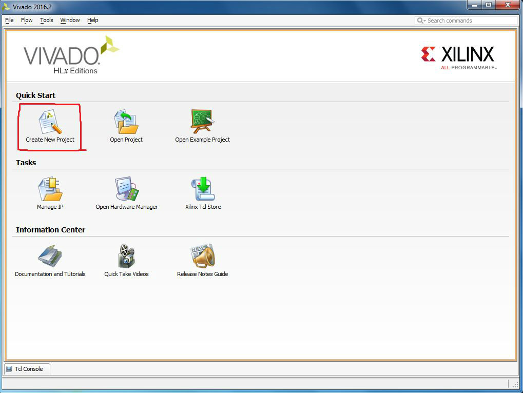
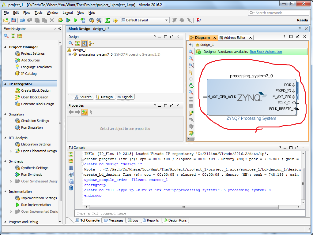
Now that the pieces are assembled, we can move on to software. The Digilent Zybo board that this tutorial uses has both an FPGA and ARM processor on board, and first we will be looking at programming the FPGA. The software used to do this is the "Vivado Design Suite", a Xilinx product, which can be installed from Xilinx's website. Also download the program "Vivado HLS", the HLS meaning "High Level Synthesis", which will be used shortly.
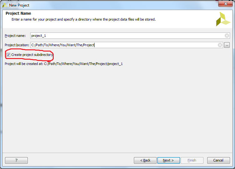
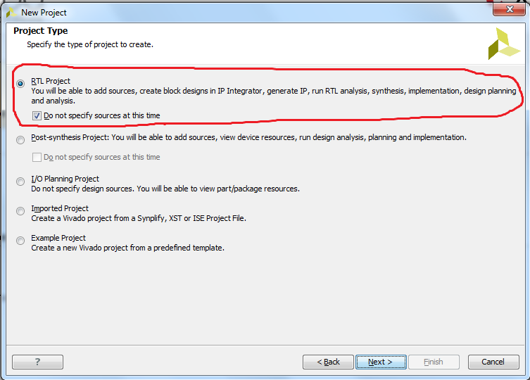
After starting up Vivado, Select Create New Project, and name it what you want (but do not use spaces). Say it will be an RTL (register transfer level) project (the first and default option), and check the do not specify sources box, and hit next.
Now to select the chip you will be working with. Search for the part "xc7z010clg400-1", which should return only 1 result, and choose that one. Then hit next
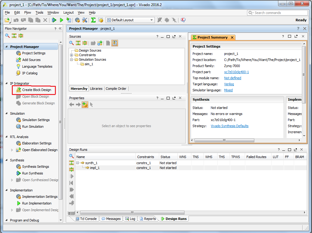
Now Vivado should open the project GUI, which may seem a bit cluttered and confusing at first, but with helpful red circles it will be easy to find the things we care about for this project. The first thing you care about is creating a block design. Click this button to Initialize an empty design.
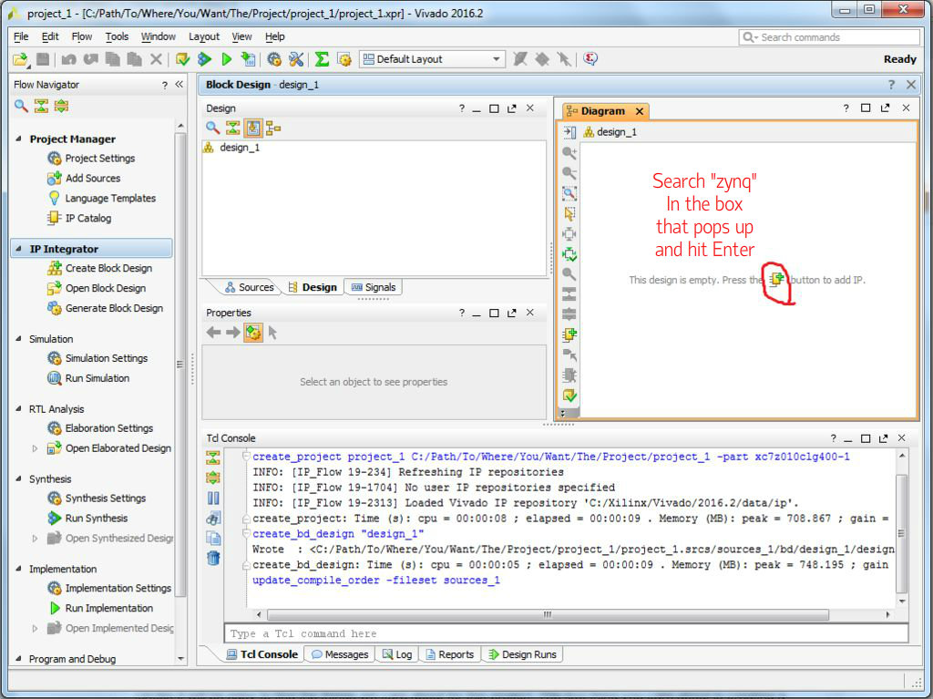
In the box that just opened, there should be a small IC icon with a green +. Click that to insert an IP. This will open a search box, which you can write "zynq" in to to find the correct IP.
Doing this inserts the Zynq processing system interface block, which is the ARM processors and several subsystems on the Zynq chip that cohabit the same die as the FPGA.
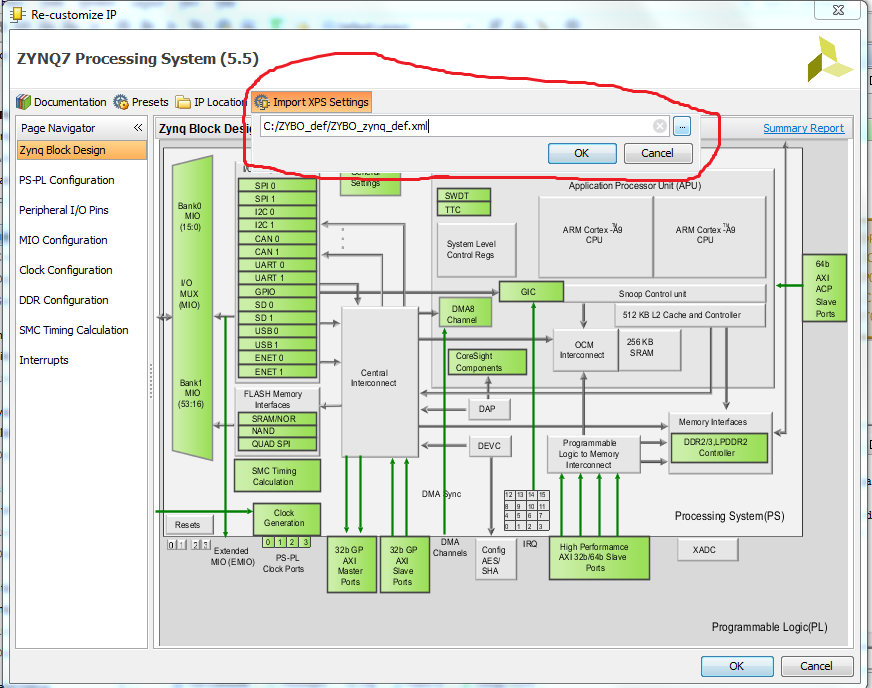
Now we need to customize the Zynq processing system. Do so by double clicking it. There are many options you can change, as you are likely seeing now, but to cover most of them we can import a board definition file, for example the ZYBO_zynq_def.xml file included in this step.
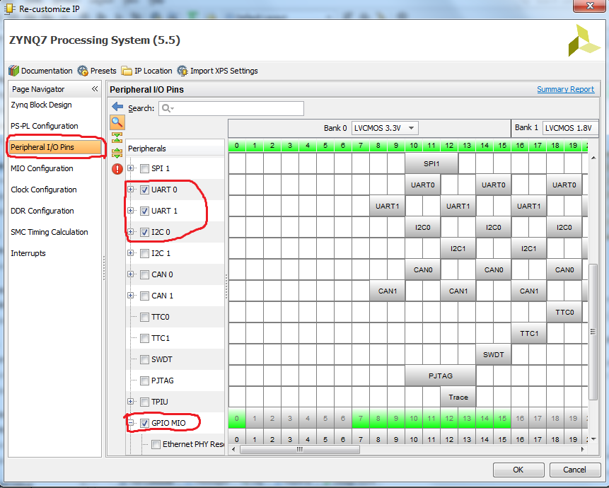
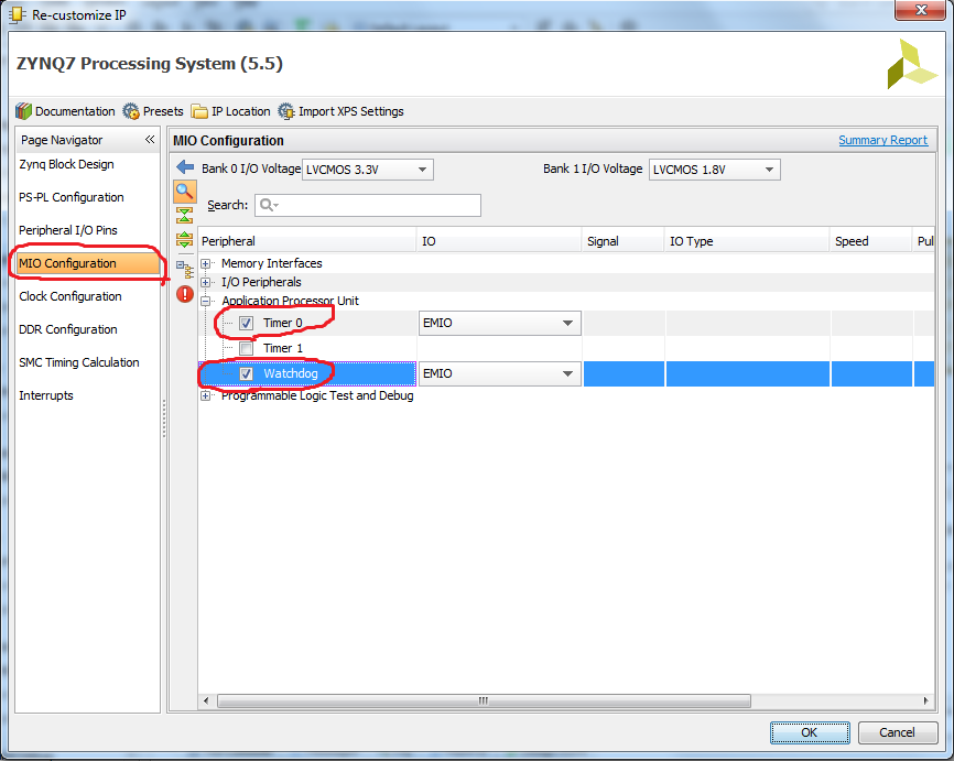
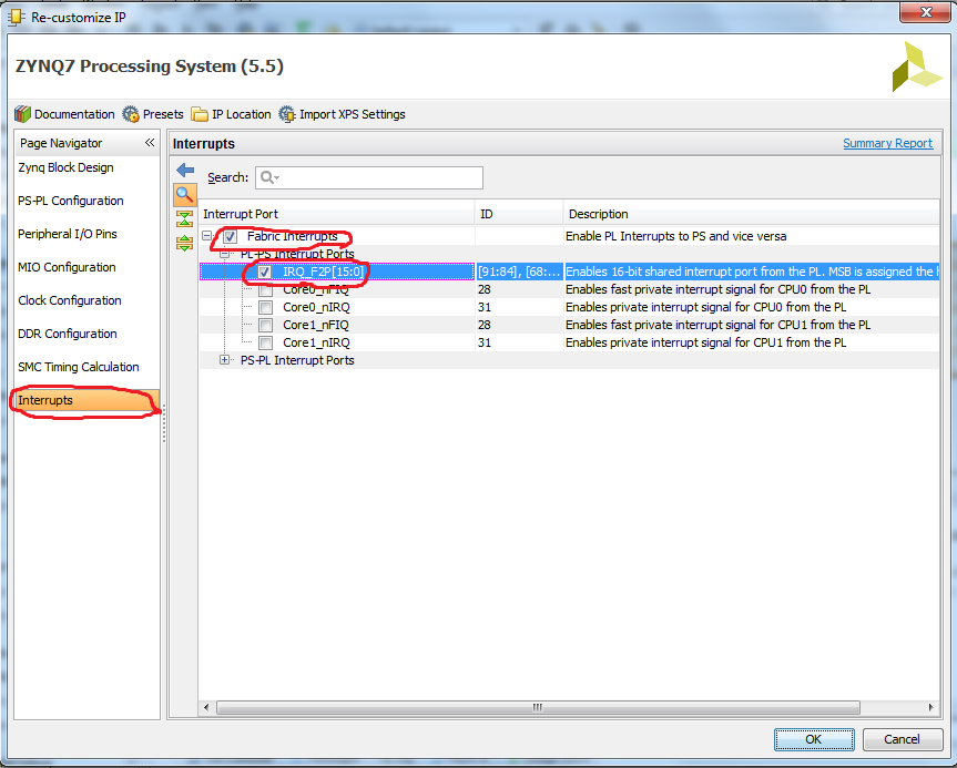
After that there are still a few options that need to be changed. Follow the images and ensure that all outlined items are checked.
In addition, import the ZYBO_Master.xdc file attached to this step. During the implementation of this design on the Zybo board, Vivado will use this file to map the I2C and UART pins to specified pins available externally on the board.
That's all we need to do for this IP, but there are more blocks that we need to add, including a special one we will have to make ourselves, which brings us to the next step
Making a Custom IP in Vivado HLS
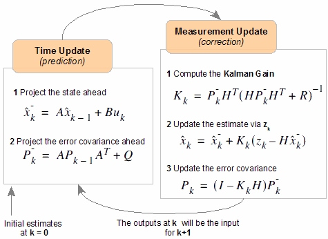

In this step we will go over how to implement a hardware accelerator for the mathematical operations needed to execute a Kalman filter.
A Kalman filter, despite the name, is more appropriately described as a cycle of controlled feedback. On a high level it involves:
1. Taking a measurement from some real data (in our case, with the IMU)
2. Using that measurement to predict some other type of data (GPS position for this project)
3. Actually measuring that second type of data with another sensor (a GPS transceiver)
4. Consolidating the predicted and actual measurements into a more reliable single piece of data (the final GPS position to log)
5. Going back to step 1, utilizing the difference in data from step 4 to better help consolidate the data on the next loop.
This process is illustrated in the included diagram. A quick look will reveal that it involves a great deal of matrix operations on floating point (non-integer) numbers. This is not something we would normally want to give a processor to deal with, especially when it is a real-time application such as this. Floating point values are notorious for taking a lot of time to manipulate, and performing this many for even a single cycle of the Kalman filter would slow down the ARM processor too much. Instead, we will take advantage of the FPGA built on the same chip! It allows us to configure hardware circuits to perform just the math operations we need using HDL (hardware design languages, i.e. Verilog or VHDL).
While we could go about implementing this in HDL by hand, it would take a lot of time. This is especially true because floating point numbers are much harder to pass around and unpack in comparison to straight integers. Instead, we will use high level synthesis of C code with Vivado HLS. High level synthesis allows us to implement the operations we need, like multiplication or division, in C. It then synthesizes the C code into HDL that can be packaged and used in Vivado designs. No need to worry about unpacking floats and routing them through math blocks by hand!
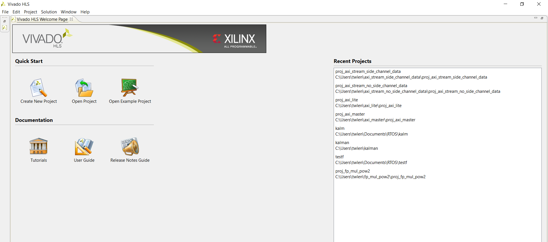
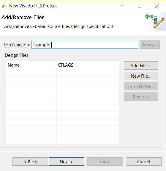
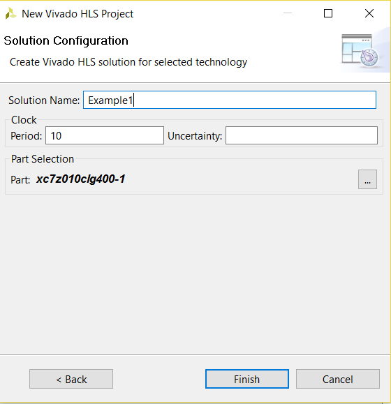
To begin, start Vivado HLS. On the first screen, select "Create New Project". A window will pop up to configure the project. Name it and place it wherever you want. The most important screens in this creation process are selecting the top level function, and selecting the correct part (both windows shown in the step pictures). The top level function acts as your "black box", and it will determine the various inputs and outputs. If you want to change it later, you can in the project settings. The part number is the same as the one used in the Vivado set up and is crucial for correct clocking and resource allocation. It is shown already selected in the image.
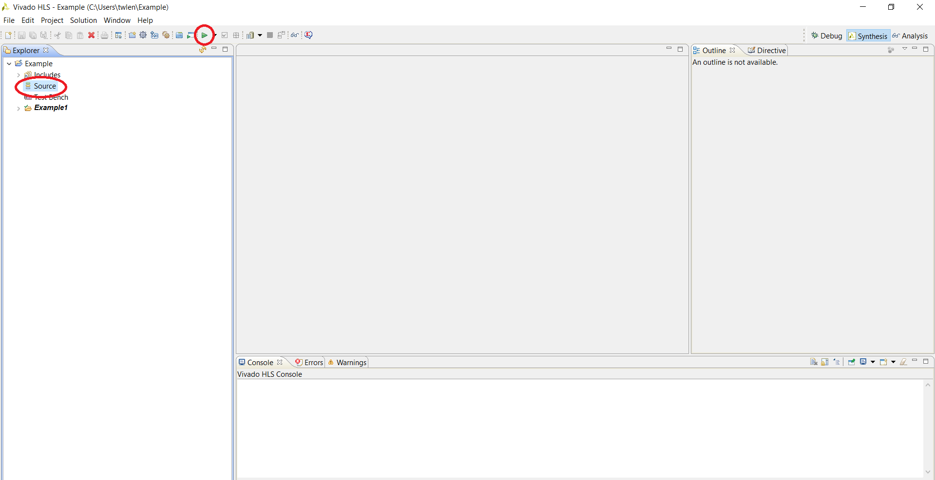
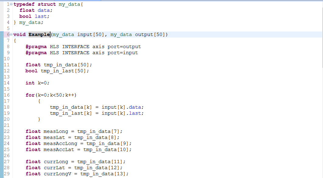
Once you finish setup, it dumps you on to a pretty barren screen. You can add a source file (to write your code and top level function) by right clicking on the "Source" entry in the left pane and selecting to either add a new file or an existing one. Once the file is created or added, you can start writing your C code! The included picture is an example of how you may want to do it. This isn't normal C code, however. There are some pretty picky rules.
First, we want to specify an interface. We will be requiring the AXI Stream interface, and that is what is shown to be implemented in the picture. The "#pragma" lines specify the input and output (the parameters of the top level function!) as requiring that interface. You may be thinking that the input and output aren't very straightforward, and you'd be right! They are arrays of the struct "my_data". This struct is needed in order to add an additional interface signal, represented by the "last" field. The actual data is carried in the "data" field.
What this function is saying is that it will take 50 floats as inputs (from the array of 50 structs, containing 1 float each, plus that additional signal), and output 50 floats in the same way. Some important things to note:
1. You should unload all of the structs at once in a loop, as shown in the picture. This is because once you read all the signals in the input, they're not going to remain, or the synthesizer might think you're attempting something you're not intending. Remember, this represents a hardware interface of streaming data. Once they're read in safely, you can shuffle and manipulate them all you want.
2. If you touch one member of the input struct from reading or writing, touch all of them at once. The reasoning is the same as 1.
3. The "last" field of the last input should go to the "last" field of the last output. This is because it will be used as the "t_last" signal in the AXI Stream interface, which signifies the last transmission.
Once you have manipulated the data and output it to your liking, you can press the green arrow on the top bar (circled in red in the diagram) in order to synthesize it. You will get 2 warnings basically saying the "data" field of the input/output structs are not included as part of the interface signals. That is what we are expecting, so it's fine. If the synthesize is successful, it will automatically pull up a summary screen of the resources it uses in the FPGA. You may browse it, but you probably just want to export the HDL into a nice little IP package to use in Vivado. You can do that by pressing the squarish icon on the top bar (circled in an included picture). For Format Selection, IP catalog is what you want.
The C file we have successfully used to manipulate floating points is attached. While it doesn't implement the covariance aspect of the Kalman Filter (yet), it does successfully demonstrate the prediction equation that uses multiple floating point multiplies and adds. Implementing the covariance part of the filter in code at this point would be just like doing it on the processor, except for all of the HLS extras wrapped around it.
Do note that our implementation drops the first 7 floats of transfer consistently each time. This may be a clocking issue with the interface on the Vivado block diagram side of things, but we have designed around it. It isn't ideal, but it is a reliable occurrence. We work around it by offsetting the start of any buffer reads or writes by 7, and then treating that offset as the real start of the buffer. Now, it's time to hook up this custom hardware to our Zynq Processing System!
Downloads
Vivado Design Suite Cont.
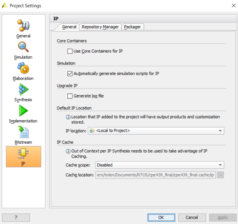
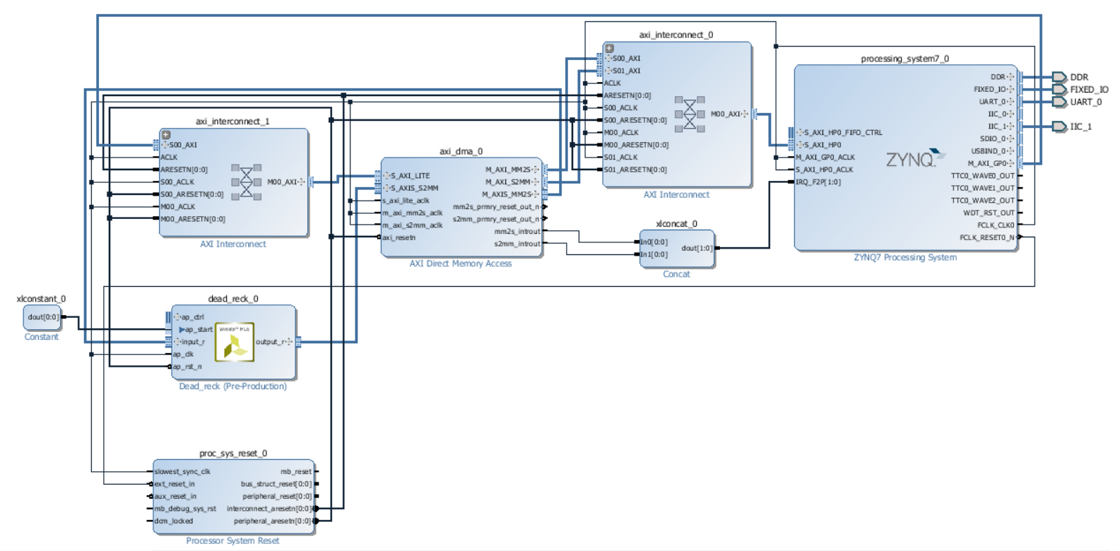
Now that we have the custom IP made, we can add it and the other ones we want to our Vivado block design. In order to have access to it, we need to add it to our IP repository. To do this, click the "Project Settings" Gear Icon on the top bar and navigate to the "IP" options in the bottom left on the window that pops up. Click on the "Repository Manager" tab, and you should be taken to a list of current added user repositories. Press on the green plus icon next to list to specify the path to our new repository. Browse to your Vivado HLS project directory from the last step. You want to seek: "Your Project Directory" >> "Your Solution Name" >> "impl" >> "ip". In this folder you can find the Verilog and HDL files of the floating point hardware accelerator we made. To add it, click on the "IP Catalog" option in the left menu. The user repositories are easy to find at the top of the list. Select the HDL file, which should be named whatever the name of your top level function was. It will now be added to the block diagram with the Zynq processing system. That isn't it, though. We need to add and route a lot of different additional blocks in order to be able to transfer data to and from our accelerator.
First, search for and add an "AXI Direct Memory Access" block like previously with adding the Zynq Processing System. This block is a controller that will write data to and from peripheral devices, placing it in system memory that the processor then accesses. It allows for moving a lot of data through a system without weighing down the expensive processor with the task. Add also an "AXI Interconnect" and a "Concat" block.
Hook the DMA block to the interconnect, and the interconnect to the Zynq block, as shown in the included step diagram. For all of these AXI connections, you will have the option of automatic wire routing. You can do it if you are careful with which blocks are connected at each step, but we preferred to hook things by hand in order to make sure nothing was miswired. Verify that the "M_AXI_MM2S and M_AXI_S2MM ports are correctly connected to the S00_AXI and S01_AXI ports on the interconnect, so that the DMA can reach the Zynq block on the other end of the interconnect. Route the xxx_introut pins of the DMA block into the Concat block as shown, and then that output into the IRQ_F2P port of the Zynq block. This enables interrupts from the DMA block to reach the Zynq processor, signalling the end of a send or receive from the hardware accelerator.
Connect the "M_AXI_GP0 port of the Zynq block either directly to the S_AXI_LITE port on the DMA, or through a second interconnect like we did in our diagram. It's not necessary if you are only using that AXI channel for one device, but it allows for later additions such as a GPIO block. Next, connect the output port of our custom accelerator block to the "S_AXIS_S2MM" port on the left side of the DMA. In addition, connect the input port of that block to the "M_AXIS_MM2S" port of the DMA. Add a "Constant" block, set it to a value of "1", and route it to the "ap_start" pin of the "ap_ctrl" port of our custom block. This should enable it to be always ready to receive streamed data, and is somewhat of a shortcut. We suspect this may the cause of the loss of the first 7 floats on every transfer, as discussed in the previous step.
That should be all of the major connections. You just need to add the Processor System Reset block, shown in the diagram, and connect all of the clocks and reset signals together. These are standard connections and can probably be safely auto-routed. Alright, now it's time to SYNTHESIZE. You can actually save a lot of time by selecting the "Generate Bitstream" option in the top bar. Not only does this implement synthesis if required, it moves straight on to generating a bit stream of hardware specs the we'll be exporting to the Vivado SDK once it finishes! Now sit back, get a coffee maybe... This might take a while. Assuming you didn't run into any errors (and haven't died of waiting), you can now select the Export->Export Hardware option in the drop down File menu. Be sure to check the "Include Bitstream" box and confirm. It should be pretty instantaneous. Now we will launch into the Vivado Software Development Kit. Hooray, we're out of the hardware woods!
Implementing a FreeRTOS Driver
With the hardware from Vivado exported, and the SDK open, we can now begin to work on a driver program to download to the ARM processor. After going to an opening screen for a short while it should automatically open the exported hardware.
Now we need to generate a "board support package". A board support package (or BSP) is a large amount of generated C files based on the hardware you exported. These are generally things like defining device addresses and configuring interrupt options, based on what you selected in the Vivado block design. This includes the information needed to communicate with the DMA controller, and our hardware accelerator in turn.
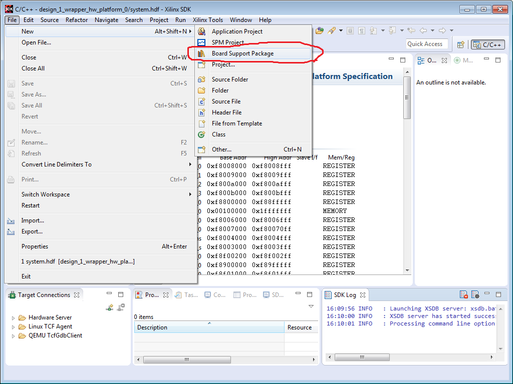
Open the File > New dropdown at the top left and select "new board support package", then hit finish without changing anything in the first dialog to pop up. This will pop up the second dialog which needs to be changed a bit. Check the "lwip" and "xliiffs" options to generate files for those, and then make this BSP.
Now, for reasons that we can only assume are some deep rooted bug, it's always been the case for us that we needed to make two BSPs before we could actually make use of them, so as a work around we recommend making another one in exactly the same way (differs only in name).
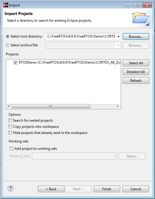
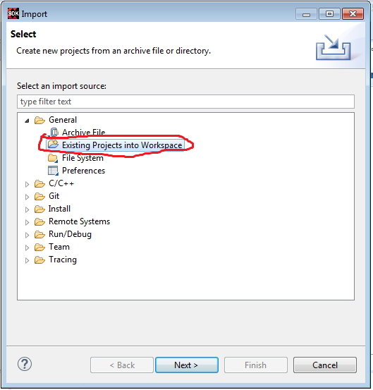
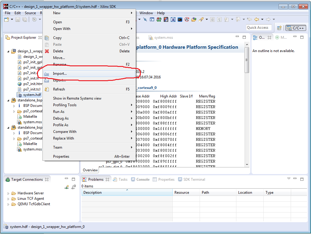
Now right click somewhere in the white space in the box on the left where all the files in the workspace are listed, and select import. Then select general > existing project. Browse to wherever you downloaded the zip file (and decompress it if you haven't already). From the top level folder, navigate: FreeRTOS >> Demo >> CORTEX_A9_Zynq_ZC702 and select it. You will get a list of projects to import. Only import the RTOSDemo. Once you import it, it will start to automatically attempt to build the project. It will fail, and that's okay because that's how we learn.
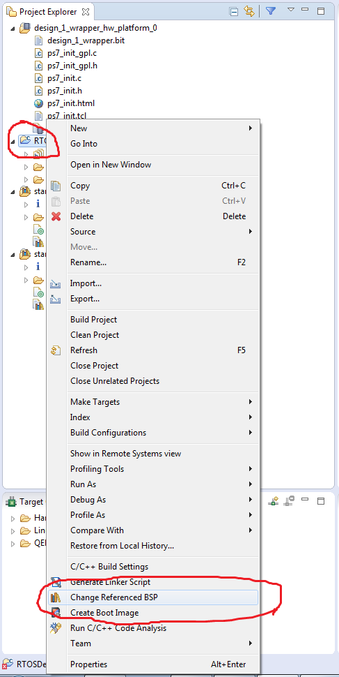
Now right click on the blue RTOSDemo folder icon just added to the list of files, and near the bottom select "change referenced BSP". This should open a pop-up with the existing BSPs. If it's empty and you only made 1 BSP try making another one that is the same. Once you can get an appropriate BSP to show up in this panel, check it and finish. It should now be able to successfully build a project that can run on the Zybo board.
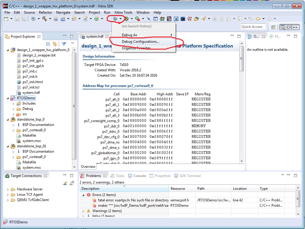
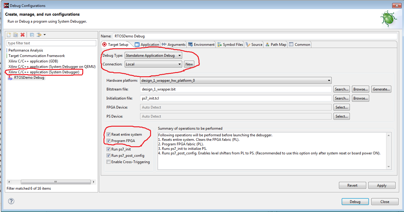
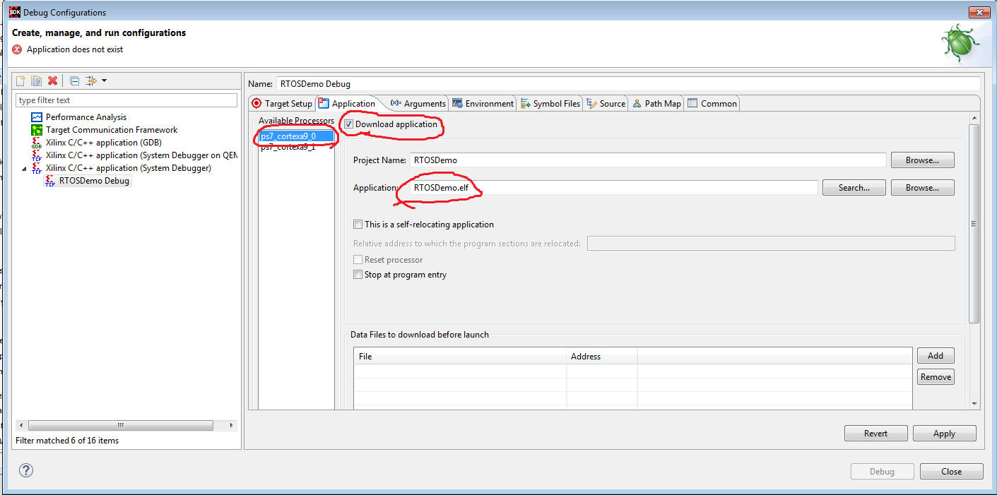
Now that we have code, we need to set the rules for running it on the ARM processor. Find the green bug icon with drop down arrow next to it (the debugger button) at the top of the screen, and open the drop down. From the menu select debug configurations. Then choose "Xilinx C/C++ application (System Debugger)" to create a new configuration. Make sure Debug type is "Standalone Application Debug" and connection is "Local". Check "Reset entire system" and "Program FPGA", then click the "Application" tab at the top. here make sure ps7_cortexa9_0 is selected, and check "Download application".
Gutting a Poor Demo
While it's a nifty demo of FreeRTOS at work, all we need is the kernel functionality. That means burn, baby, burn! Attached to this guide is a zip file of all of our source files used in developing this project. This includes a modified main.c, so we need to remove the existing one first. This might sound like a scary thing to do, but you can always save the old one if it makes you anxious. Once your backup is made, right click the main.c file in the RTOSDemo project and select to delete it. If there is an option to remove it from disk, select it. This is to prevent it interfering with our new main.c we will be importing. Speaking of importing, do just that! The files listed below are all of the utility functions you'll find helpful in coordinating communications with the sensor and our custom hardware. Note that all of them (besides main.c) begin with an "sf_" prefix (short for "sensor fusion") in order to assist in more easily identifying our user files when working in the project. Although each file here has a short description, they are each thoroughly commented and more informative to read than explaining it here. These files are:
sf_main.c: Once the main.c file has finished setting certain parts of the system, it will launch to the beginning of the sf_main.c function. This can be treated like the normal main of this project. This file contains the setup for each FreeRTOS tasks, sensor initializations, and the tasks themselves.
sf_coms.c/h: This file contains the helper functions for initializing, writing to, and reading from UART and I2C. Although there are also specialized reading and writing functions pertaining to each sensor in other files, the IME and GPS sensors can essentially be talked to solely with these.
sf_imu.c/h: Contains functions for initializing and communicating with the IMU sensor over I2C. Additional register addresses of the IMU can be defined in order to add more functionality later if you want.
sf_gps_settings.c/h: Contains the commands to communicate with and configure the GPS transceiver (as opposed to just letting it stream data and listening in).
sf_gps.c/h: Not actually for communicating with the GPS transceiver, but parsing and processing the data that we get from it.
sf_sd_card.c/h: All the functions for initializing, reading, and writing the Zybo board SD card. Includes a test function to verify correct operation.
sf_dma.c/h: The functions for configuring the DMA controller, and reading to and writing from the hardware accelerator using DMA.
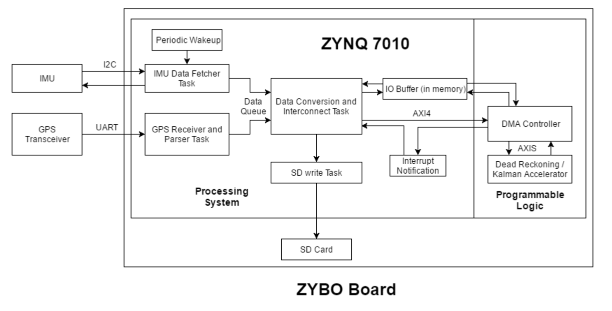
The system diagram included in this step shows each of the system tasks running in sf_main, as well as how they use the above software libraries in relation to the subsystems and hardware. Feel free to browse each task and tweak what they do to fit your needs. The core libraries are there to enable functionality and allow for easy additions to the existing project.
Downloads
Testing the Sensors
Included in the sf_main.c function is a #define TEST statement at the top of the file. If TEST is defined as a non-zero value, then the sensor test version is enabled. If TEST is 0, then the full version is. In the test version, the sensors are calibrated and read out to serial to help you determine if they work. The DMA is also tested. In the full version the entire flow including reading from sensors, doing math in the FPGA, and logging outputs to files on the micro SD card are all set up.
We recommend that you run in test mode first, to make sure you get useful data from the sensors. Connect the USB cable between your computer and the Zybo board, and open a serial terminal (such as putty) connected to the COM port that the Zybo is on. You can check which COM port the Zybo is on by checking your device manager, and looking for "serial communication" in the list of COM ports. The correct baud is 115200. With serial set up you should begin seeing repeated outputs of the IMU for calibration. Once the calibration is to your liking (discussed below), press any key to see looping test output of DMA transfers, GPS sentences and IMU data.
In the source code you can see where raw numbers are put into the DMA TX buffer and received back into the RX buffer. These buffers are then printed to demonstrate the hardware accelerator correctly performing floating point math. Feel free to input your own numbers to try out. The hardware accelerator right now is only implementing the dead reckoning portion of the Kalman filter.
The output GPS sentences are GPRMC, correctly parsed and checked for validity. If the GPS transceiver is not sending valid data, you will not see any output from it. Since it can take sometimes 20 minutes to get a GPS fix, don't be alarmed if it doesn't happen right away. The IMU data is simply a raw compass heading, followed by raw acceleration data from the the IMU for each axis. Interpreting the NMEA standard, you can manually compare the GPS coordinates to your known coordinates (derived from a trustworthy source) to see if the GPS is giving accurate readings. The IMU data is 1 m/s^2 / 100 LSB, so you should see about 980 on whatever axis is receiving the gravity vector. If you wish to test the SD card functionality, you must insert the initialization and test function yourself at the start of sf_main. Anytime before the scheduler startup is actually okay.
Note that compass data is not valid unless the calibration status is reporting anything '3' or greater in the right nibble of the hex value. To calibrate, move it in a figure 8 pattern in the air. Accelerometer calibration is best when the left nibble of the hex value is 'F', achieved by placing it static on several different sides.
Satisfied with these results, you can define TEST to 0 and dive head in. As mentioned at the start of this guide, we ran out of time to fully implement the desired functionality, but we were able to demonstrate each subsystem's correct behavior, which is most of the journey. The system diagram shown in the last step is still implemented; Some conversions/calculations may be incorrect, but the flow of logic should not have to be altered. The hardware accelerator only implements a simple dead reckoning algorithm right now, but the addition of a covariance matrix to adjust the results of the dead reckoning would be straightforward in C code. The parameters for the Kalman filter are well-documented online, and will linked to below. In addition, the IMU and GPS datasheets are linked if you wish to utilize the coms functions to further extend the project. We hope you've found it interesting!
Information Resources: Kalman Filer with GPS, IMU Datasheet, GPS Transceiver Datasheet.