SUPER Nintendo Entertainment System Controller XL
by Arnov Sharma in Circuits > Raspberry Pi
1543 Views, 12 Favorites, 0 Comments
SUPER Nintendo Entertainment System Controller XL

.gif)

.gif)
.gif)

Hello everyone, and now I have something really exciting to share with you all: the SNES XL, an enlarged version of the well-known SNES controller that has functional buttons exactly like a standard SNES controller for playing retro games.
It is arguably the largest SNES controller in the world, judging by its size (I am not sure if that is accurate).
Designed entirely in Fusion360, the controller's enormous size required us to split it into three separate parts, each of which we had to print individually before assembling them into one huge body.
We used 12 mm x 12 mm tactile switches soldered on some specially designed PCBs that were also created from scratch.
The primary MCU, the XIAO M0, imitates a game controller device using the HID standard.
The controller is merely an enlarged version of the same idea used in a previous project of mine.
https://www.instructables.com/Arduino-Game-Controller-for-NES-and-GBA/
This article is about how this project was built, so let's get started.
Supplies
The following were the materials used in this build-
- Custom PCBs Provided by PCBWAY
- 3D-Printed parts
- Super Glue
- Tactile Switches
- Wires
- Threaded Inserts M3
- Soldering Iron
- XIAO M0 MCU
ABOUT THE OG CONTROLLER


The Super Nintendo Entertainment System (SNES) controller is a classic video game controller that was designed and released by Nintendo in 1990.
It was the primary input device for the SNES, a popular 16-bit gaming console that gained widespread popularity during the early 1990s.
The SNES controller features a distinctive design, with a rounded shape and a cross-shaped directional pad (D-pad) on the left side for movement control. On the right side, there are four action buttons arranged in a diamond pattern, typically labeled A, B, X, and Y. These buttons are used for various in-game actions, such as jumping, attacking, and interacting with the game environment.
In addition to the main buttons, the controller includes two shoulder buttons, L and R, located on the top edge. These shoulder buttons added new gameplay possibilities by providing additional input options. The Start and Select buttons, positioned in the middle of the controller, are used for pausing games and accessing in-game menus.
The SNES controller has become an iconic symbol of retro gaming, and its design has influenced subsequent generations of video game controllers.
Many classic games, including Super Mario World, The Legend of Zelda: A Link to the Past, and Super Metroid, were designed to be played with this controller, contributing to its lasting legacy in the world of gaming
DESIGN BREAKDOWN
.gif)
.gif)


This project's 3D design begins with an original SNES controller image that is imported into Fusion360. The controller's width is calculated by calibrating the image and making it 471mm from side to side.
The controller's shape was then created using the enlarged image, and the body was then made hollow using the shell command.
Buttons were then modeled by using the same imported image.
Every button has a PCB attached to the rear that houses a tactile push button. The PCB is positioned so that there is a 1 mm space between the top side of the push switch and the bottom side of the 3D-printed button.
The entire 3D part descends by 1 mm when we press the button, toggling the push button and allowing us to view the button press.
In the same way, the Push Button PCB is present in every button, including the D Pad, ABXY, Start, and Stop buttons.
With the exception of the DPad, each button has a single PCB with a single push button. The DPad has a square PCB with four push buttons.
PCB DESIGN


Following design completion, we export the layout for each board and utilize it to model three distinct PCBs: the XIAO MCU Breakout board, the DPad board, and the single button board.
Three schematics were prepared for each board.
First, we create the DPad schematic, which consists of four Tactile push buttons, pin 2 of which is attached to a CON1 port and pin 3 of each of which is connected to GND.
Next, we export the netlist and create the PCB for the DPad board. The CAD design's exported board layout was used to create the PCB's outline for the DPad.
Switches were placed according to the CAD layout.
Next, we set up the schematic for a single switch board, which had four CON1 ports connected to a single tactile switch.
Pin 3 of the Tactile switch is connected to two CON1 ports, which will be connected to the I/O pin of XIAO, and Pin 2 is connected to two CON1 ports, which will be the ground port.
After that, this schematic was turned into a PCB design, which was created using an outline from a CAD model.
Finally, the XIAO Board is ready. It was constructed in a manner similar to the other two PCBs, starting with the schematic, which was then converted into a PCB design and the board's layout was created using the outline from Cad
PCBWAY SERVICE
.gif)
.gif)

After the PCB design was completed, Gerber data was generated and then sent to PCBWAY for samples.
For this project, we made three different-shaped PCBs so three orders were placed in white solder masks and black silkscreen.
The PCBs were received within a week, and they were excellent, as expected.
I really love the quality of PCBs made by PCBWAY. There are other manufacturers available, but their service is always on another level.
check out PCBWay service for getting great PCB service at a lower cost
BUTTON PCB ASSEMBLY PROCESS
.gif)
.gif)
.gif)
.gif)
.gif)
.gif)
First, we begin the extremely simple PCB assembly process for the XYAB button PCBs.
- The tactile switch is added to the switch pads on the PCB, and the process is repeated for each of the four boards.
- After that, we solder the four pads on each PCB to permanently attach the switch, and we repeat this process for every PCB.
- Following the construction of the XYAB Button PCB, we take the Dpad PCB and solder the switch pads from the bottom side after adding four switches to the switch pads.
Switch PCBs are now ready.
XIAO MCU Breakout Board ASSEMBLY PROCESS
.gif)
.gif)
.gif)
- We utilize two CON7 female header pin connectors for the XIAO MCU Breakout Board, adding them to XIAO Pads.
- The board is then turned over, and the connector pads are soldered to permanently link the connector to the PCB.
- Now that XIAO is finally installed in the female header pin connector, the XIAO MCU Breakout PCB is assembled.
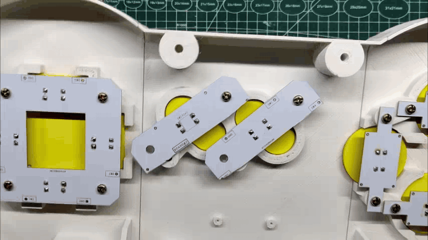
BUTTONS PCB & XIAO BOARD
.gif)
Eight single switch PCBs—for X, Y, A, B, Start, Stop, L button, and R button, respectively—will be used for the assembly.
The D Pad Assembly will use a single square PCB with four buttons on it.
Next, the XIAO MCU Breakout Board is utilized to link each PCB to the XIAO I/O pins.
Every board has pads that are linked to switch pins; all we have to do to complete the wiring is connect GND to every switch PCB and each switch's other pin to the IO pins on the XIAO board.
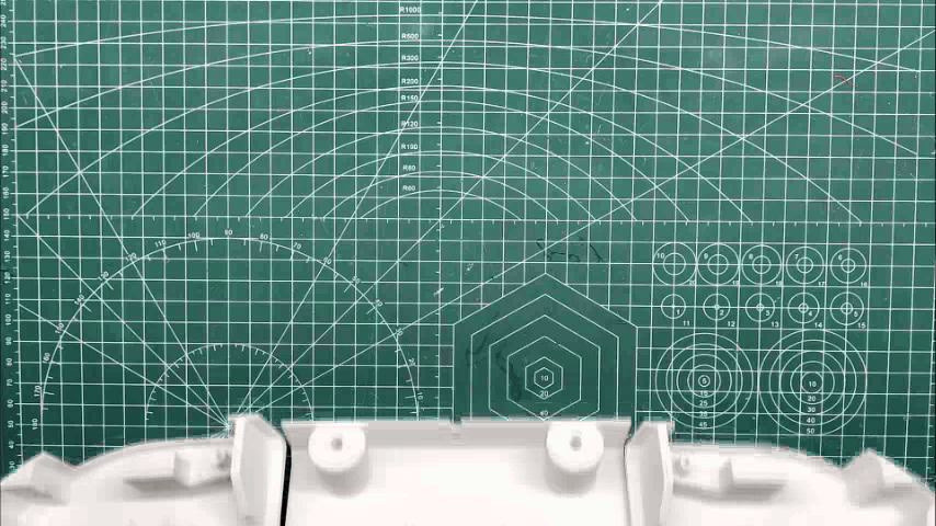
3D-Printed Parts
.gif)
.gif)
Because the controller is 471 mm by 200 mm in size, it cannot be printed with a standard 3D printer. To solve this issue, we split the body into three separate pieces and printed each one separately using an Ender 3 printer and white PLA..
Because the body is only 2 mm thick, we only need to print this part in standard 20% infill. In order to cut down on print time, we switched from a typical 0.4 mm nozzle to a 0.8 mm nozzle. Printing each part took about 13 hours when we used the 0.4 mm nozzle, but only 6 hours when we used the 0.8 mm nozzle.
The D pad button was the first to be printed using yellow PLA and a 20% infill using the same 0.8mm nozzle; the remaining buttons were printed using red PLA.
BODY ASSEMBLY PROCESS
.gif)
.gif)
.gif)
.gif)
.gif)
.gif)
Let us have a look at the super glue we will be using before we get started.
We are using Feviquick 203, which is a cyanoacrylate adhesive with low viscosity and fast setting for rubber and plastic.
Although Feviquick is well-known in India, there are other options that can be utilized.
- Using fiber tape, we first join two parts together from the front side to begin the assembly process.
- Next, we fill the space between the two parts from the inside face with super glue.
- We repeat the process on the other side, allowing the adhesive to dry and solidify for ten to fifteen minutes.
- After the glue solidifies, we remove the fiber tape and the result of this process will be a solid body that is made from three different 3D-printed parts.
This project can also benefit from an extra stage that involves using epoxy to fill the space between the two halves, sanding the epoxy, applying primer to the entire body, and then applying a couple coats of paint.
THREADED INSERTS PROCESS
.gif)
.gif)
.gif)
.gif)
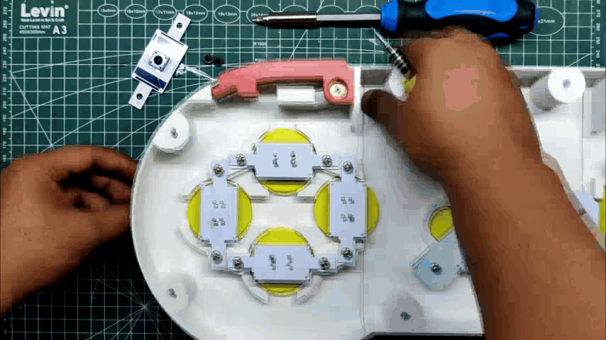
Threaded inserts of the M3 size are used to mount PCBs on the 3D printed body.
These inserts are placed into holes that are added to the 3D part. They serve to facilitate the insertion of bolts or screws and make it easy to remove them for reuse at a later time.
To position the Switch PCBs, we needed to employ a total of twenty threaded inserts; each board will have two inserts mounted on it, and the DPad has four threaded inserts for mounting.
Using a tweezer, we first choose the insert and position it in the 3D body's hole.
Next, we heat the insert with a soldering iron set to a temperature of 150°C. Once heated, the insert fits into the hole when the plastic in front of it melts.
It thus slides into place, and after we take out the soldering iron, it cools down and is fixed there permanently.
D PAD BUTTON ASSEMBLY
.gif)
.gif)
- Prior to assembling the buttons, we mount the DPad button in its designated location and attach the DPad PCB to the rear of the 3D buttons.
- Next, we permanently fasten the PCB in place using four M3 bolts.
- We verify whether or not the button press is smooth.
XYAB BUTTONS ASSEMBLY
.gif)
.gif)
- The round buttons were then placed on the base body in the ABXY position, and the Switch single-board PCB was positioned on the back of the buttons.
- Following the installation of eight M3 bolts to secure every PCB in place, we tested the buttons to see if they were functioning correctly.
START/STOP BUTTONS ASSEMBLY
.gif)
.gif)
- After that, we placed START/STOP Buttons there and attached the switch PCB to the rear.
- Next, we permanently put the PCB in its place using four M3 bolts.
L & R BUTTONS
.gif)
.gif)
.gif)
.gif)
.gif)
.gif)
.gif)
.gif)
.gif)
- The Left button is then positioned in its proper location and fastened there using an M2 screw.
- Next, we put the single switch PCB directly to the 3D body by mounting it vertically with the Left Switch using two M3 Screws.
- Following a check of the switch press, we install the R button in its designated location, repeat the process of attaching the button with an M2 screw, and then add the switch PCB vertically in its designated spot.
Both Left and right button are now finalized.
BUTTONS TESTING
.gif)
We use a multimeter set in continuity mode to test the button connections. We attach one wire of the multimeter to the switch's GND port and another wire to the other pin of the switch.
when we press the tactile button, multimeter beeps which means GND is being connected with the other pin of button which means the button is functioning perfectly.
we checked all buttons with this process.
ADDING XIAO BOARD
.gif)
.gif)
Next, we place XIAO Breakout Board in its place and use two M2 Screws to secure it in its place.
XIAO Breakout board has been placed in its place and now we can move onto the next step which is to wire everything together.
WIRING


When the digital pin is pushed through the switch and the key is pressed, our setup functions.
We are using total of 12 Tactile buttons in this built which are each connected to a Digital Pin of XIAO MCU.
Total Three PCBs are used in this project, the DPad PCB consists of Four Tactile buttons.
Then we have the single button PCB and the XIAO Breakout Board.
All button's PIN 1 are connected together with GND Pin of XIAO, this pin will be the common ground.
L Button is connected with Pin D0 of XIAO, UP is connected with D1, LEFT is connected with D2, RIGHT is connected with D3, D4 of XIAO is connected with DOWN, START is connected with D5, X is connected with D6, Y is connected with D7, A is connected with D8, B is connected with D9 and the R Button connected with D10 of XIAO.
STOP Button is not connected to any PIN as XIAO only have 11 I/O Pins which can be use.
CODE
This code configures digital pins for button inputs, reads their states, and uses the Gamepad library to simulate a game controller based on the button states. It's designed to be part of a project where the Arduino is used to emulate a game controller.
Here's a breakdown of the code:
#include <Gamepad.h>
Includes the Gamepad library, which is likely a custom library or part of a third-party package for handling gamepad input.
Gamepad Initialization
Gamepad gp;
Creates an instance of the Gamepad class named gp. This instance will be used to simulate the game controller.
Pin Configuration
void setup() {
  // Pin configuration for buttons with INPUT_PULLUP
  pinMode(0,  INPUT_PULLUP); //LEFTBUTTON
  pinMode(1,  INPUT_PULLUP); //RIGHTBUTTON
  pinMode(2,  INPUT_PULLUP); //UP
  pinMode(3,  INPUT_PULLUP); //DOWN
  pinMode(4,  INPUT_PULLUP); //LEFT
  pinMode(5,  INPUT_PULLUP); //RIGHT
  pinMode(6,  INPUT_PULLUP); //A
  pinMode(7,  INPUT_PULLUP); //B
  pinMode(8,  INPUT_PULLUP); //START
  pinMode(9,  INPUT_PULLUP); //STOP
}
In the setup() function, the code configures digital pins as inputs with pull-up resistors. These pins are used to read the state of buttons connected to the Arduino board.
Button State Reading and Gamepad Simulation
void loop() {
  // Variables to store button states
  int UPLEFT, UPRIGHT, UP, DOWN, LEFT, RIGHT, RIGHTBUTTON, LEFTBUTTON, A, B, START, STOP;

  // Read button states
  RIGHTBUTTON = digitalRead(0);
  LEFTBUTTON = digitalRead(1);
  UP = digitalRead(2);
  DOWN = digitalRead(3);
  LEFT = digitalRead(4);
  RIGHT = digitalRead(5);
  A = digitalRead(6);
  B = digitalRead(7);
  START = digitalRead(8);
  STOP = digitalRead(9);

  // Simulate gamepad button presses based on button states
  // The Gamepad library is used to set the state of each button
  // based on whether the corresponding Arduino input pin is LOW (button pressed) or HIGH (button not pressed)
  if(UP == LOW)
    gp.setButtonState(2, true);
  else
    gp.setButtonState(2, false);

  // (Similar logic for other buttons)

  // A small delay to avoid rapid button presses
  delay(20);
}
In the loop() function, the code reads the state of buttons from digital input pins and uses the Gamepad instance (gp) to simulate the state of each button. If a button is pressed (its corresponding pin reads LOW), the setButtonState function is called to set the corresponding button state to true; otherwise, it is set to false.
Downloads
TEST
.gif)
Once the sketch has been uploaded, we connect the controller to the PC, launch Device Settings, and the Seeed XIAO M0 MCU will appear as a gaming controller icon.
We right click on the Game Controller Icon and open its settings which will show controller properties.
Any button on the controller that we press causes the button in the properties menu to change color, indicating that the setup is functioning and the button is sensed.
RUNNING RETRO GAMES: POWER Pi (RASPBERRY PI BASED EMULATION STATION)
.gif)

We are using Power Pi, a device we created a few weeks ago, for retro game emulation.
As the name suggests, Power Pi is a lightweight, integrated Raspberry Pi Dock that powers the Pi wirelessly thanks to an internal lithium-ion battery pack.
RecalBox is the emulator OS that is being used, and a Raspberry Pi 4 has been utilized in this Power Pi.
Check out the full article for more details about Power Pi-
DOES IT RUNS DOOM?
.gif)
.gif)
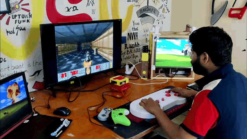
As the project's last test, we used the POWER PI to run Classic DOOM and play the game with the SNES XL Controller.
I had to set the controller down on the table and use the keys to play the game because it was too big for me to control in the air.
We had to map the controller's keys in the Recalbox OS controller settings before we could start playing the game.
CONCLUSION

.gif)
.gif)
Here is the finished product of this GIANT build: the SNES XL Controller, which allows us to play nearly every SNES game ever created, including Doom and Super Mario Bros.
The sheer magnitude of this project makes everything extremely cool, thus even though we had to model the switches from scratch due to its large size, it was well worth it.
Although I do own a standard-sized SNES controller, it is nothing like the SNES XL Controller.
This project uses an XIAO MCU, but any MCU that supports HID can be used in its place. For instance, we could create this project with an Arduino Leonardo, Micro, Pro Micro, or even an RP2040.
That is everything for now, everyone. I appreciate you reading this far, and I will be back soon with a new project.
A special thank to PCBWAY for supporting this project; visit them to get a wide range of services, including CNC and PCB services.
Peace.