Reverse Engineering a Small Amplifier
by Josehf Murchison in Circuits > Electronics
6312 Views, 78 Favorites, 0 Comments
Reverse Engineering a Small Amplifier
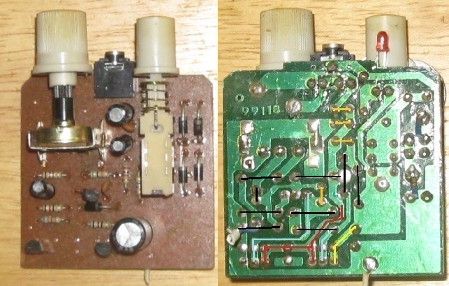
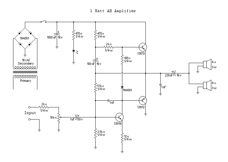
My other Instructables on reverse engineering is on components you cannot get datasheets and pinouts for. I reverse engineer a couple circuit boards a week, small ones like these take me about a day to reverse engineer and strip for their useful parts. Over time I have built up a large number of schematics and components for every kind of household electronics device imaginable.
The first circuit here is a transistorized 1 Watt AB amplifier for an external computer sound system. I skipped the ear phone jack that cut off the speakers because I felt it was not necessary for someone to replicate the circuit. And I skipped the service voltage in the schematic because service voltage changes from place to place. The voltage on the secondary winding is the important voltage for someone that wants to replicate the circuit.
The second amplifier in this Instructable; I will be reverse engineering in steppes, is a two channel 2.5 watt IC stereo amplifier for an external computer sound system.
Tools
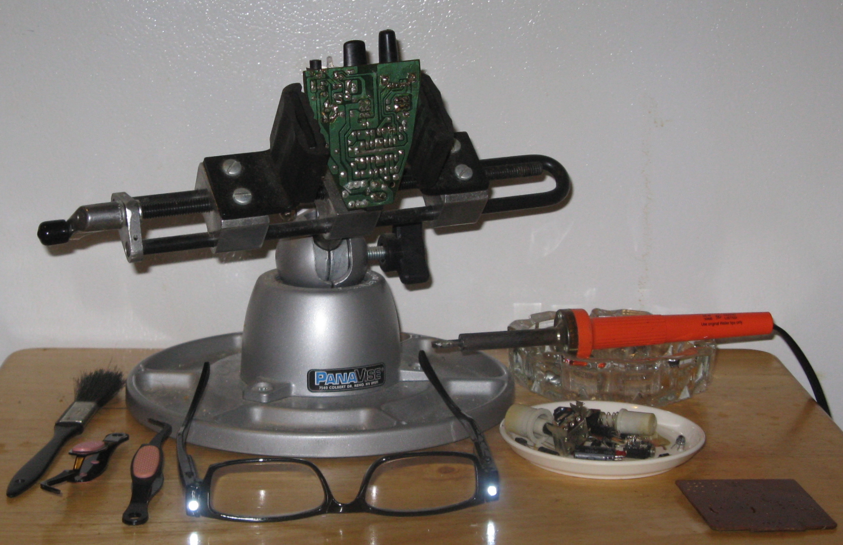
To reverse engineer a simple circuit these are tools you will need:
Camera.
A computer with internet access, the two main programs I use are Paint and Serif PhotoPlus.
Resistor Color Code, see pdf CIPC Color Codes.
Capacitor Codes, see pdf Capacitor Codes.
Datasheets on semiconductors, if you don’t have them already go to these sites to down load datasheets for free.
Diodes can be hard to read the part numbers when the diode is attached to the circuit board, so it may be necessary to remove the diode from the circuit board. The tools needed to dissemble the circuit board for salvaging its components and reading part numbers are:
Safety Glasses mine have LED lights for better viewing.
PanaVise 350 Multi-Purpose Work Center.
Soldering Iron.
Spring loaded tweezers to hold components while you desolder components.
Brush to sweep away solder.
Dish to hold components.
Photographing the Circuit Boards
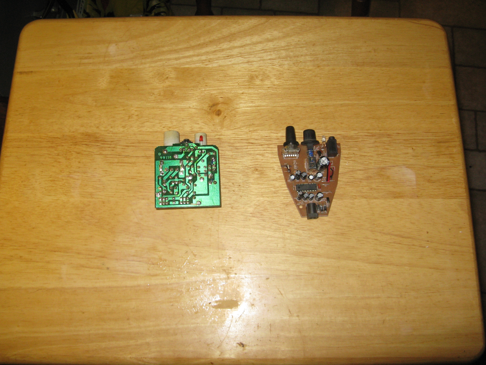
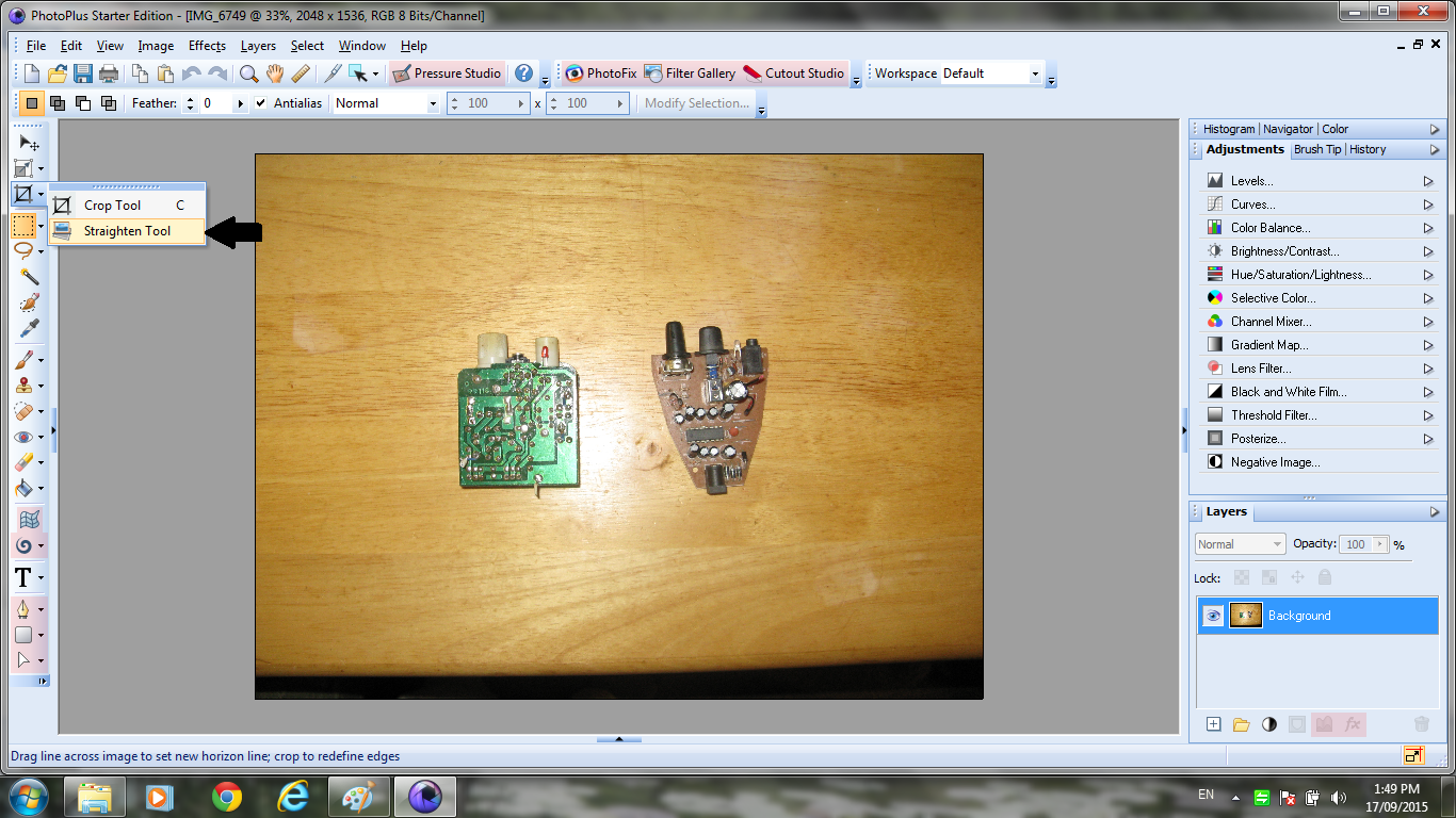
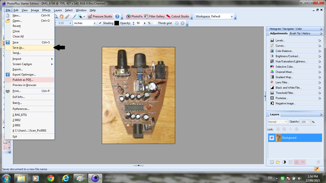
Start by photographing the circuit boards top and bottom; you want good clear photographs of the circuit boards. I like photographs with the same edge of the circuit board to the top, but if it is not the same edge to the top you can rotate and straighten the image in a graphics program. Once you have photographs of the circuit boards, load the photographs into your computer.
Next open a graphics program that allows you to straighten and crop the photo, then open the photo in the program. For this I used Serif PhotoPlus because it allows for adjustments less than 90⁰ rotation.
Find a straight edge on the circuit board and straighten the photo then crop the photo to the circuit board and save.
Do this for both sides of the circuit board.
Paint
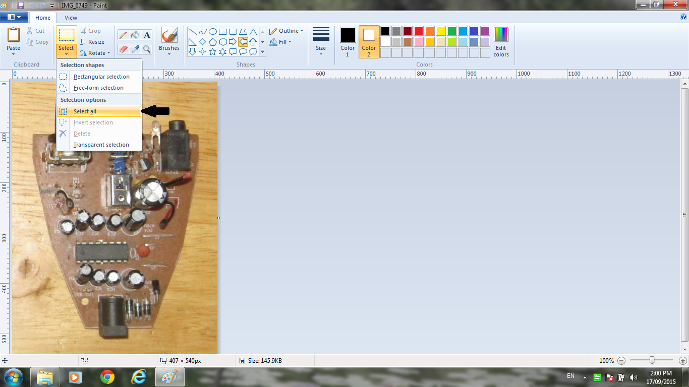
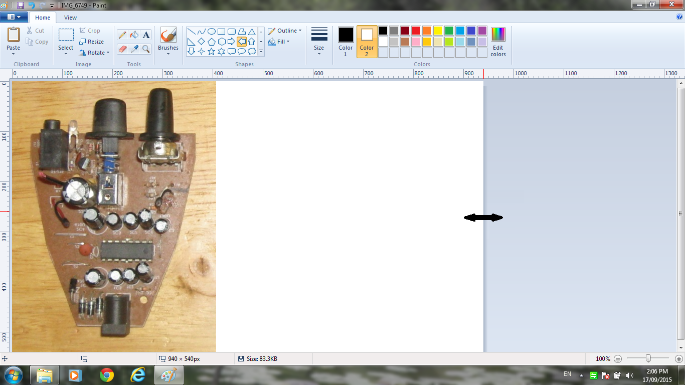
Once you have saved the straightened and cropped images close your graphics program and open the paint program.
Open the Image of the top or the bottom of your circuit board.
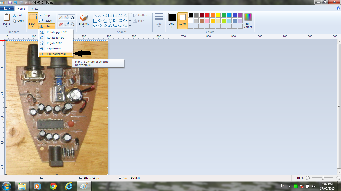
Click on select all or press CTRL + A on your keyboard.
Then click on Flip Horizontal, the reason you do this is so the position of the components on the top will be in the same position as the conductors on the bottom.
Next expand the size of the pallet by left clicking the mouse button and holding the button down with the pointer on the edge of the pallet and moving the edge of the pallet over until you have enough room for the image of the other side of the circuit board and save.
Connecting the Two Photos
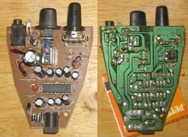
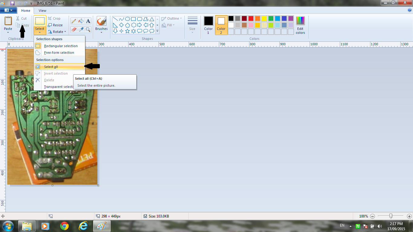
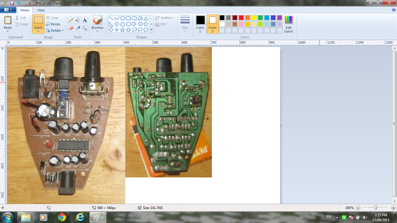
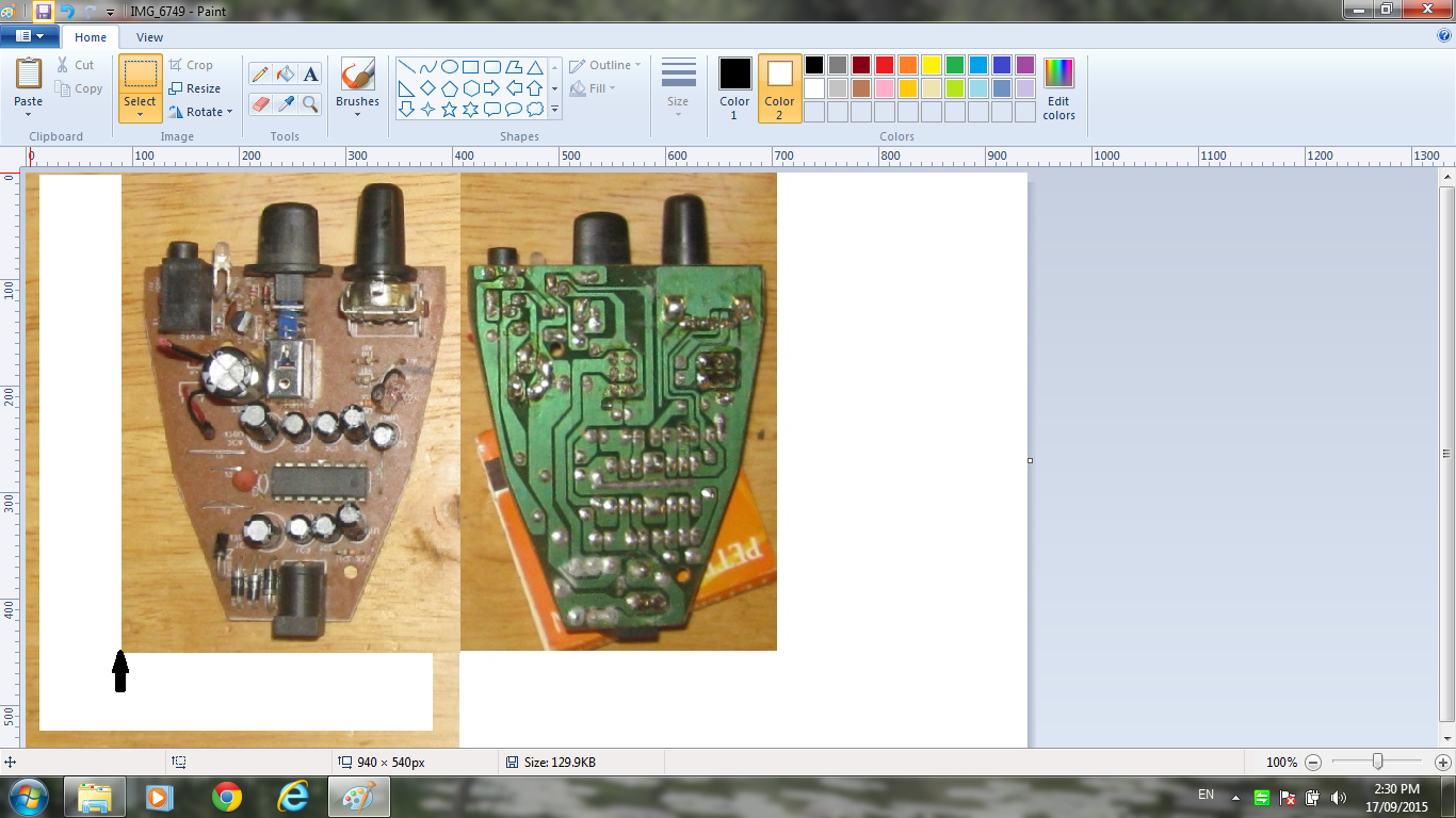
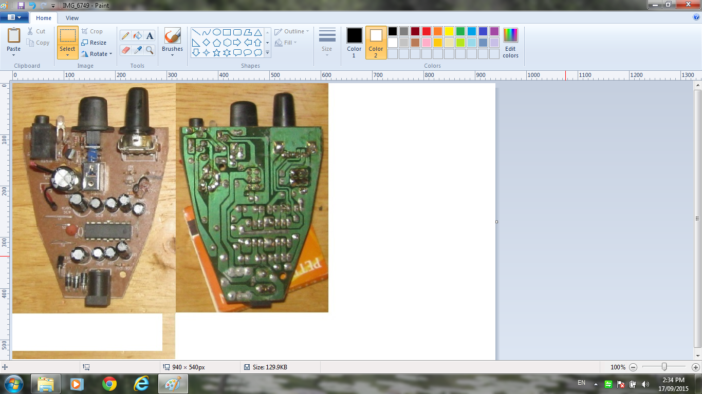
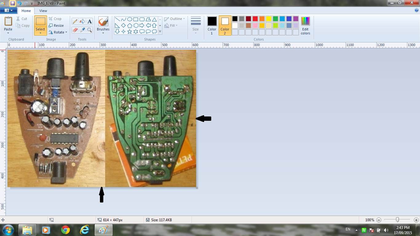
Open the photo of the other side of the circuit board select all and copy.
Switch to the photo with the expanded pallet and paste the photo into the blank space of the pallet.
By mow you have discovered one photo is larger than the other photo, this happens almost every time I do this. To fix this I adjust the size of the larger photo to match the smaller photo. I resize the larger photo so I do not loose detail. If you resize the smaller photo to the size of the larger photo it can blur the details.
Select the aria of the larger photo you want to match to the smaller photo.
Left click on the mouse button with the pointer in the center of the selected aria, and holding down the mouse button move the selected aria next to the smaller photo.
Move your mouse pointer to the corner of the selected aria, in this case the bottom left. Click on the left button and holding it down move the corner of the selected image in to resize the selected image to the size of the smaller image. When you move the corner both sides of the corner move in equally.
Next select all and move the two images to the top left corner of the pallet.
Then just as you did when you expanded the pallet move the bottom and the right side of the pallet in until all you have is the images of the top and bottom of the circuit board and save.
Now you have an image you can compare the conductors to the components on the circuit board as you trace and make a schematic.
Tracing the Circuit Board
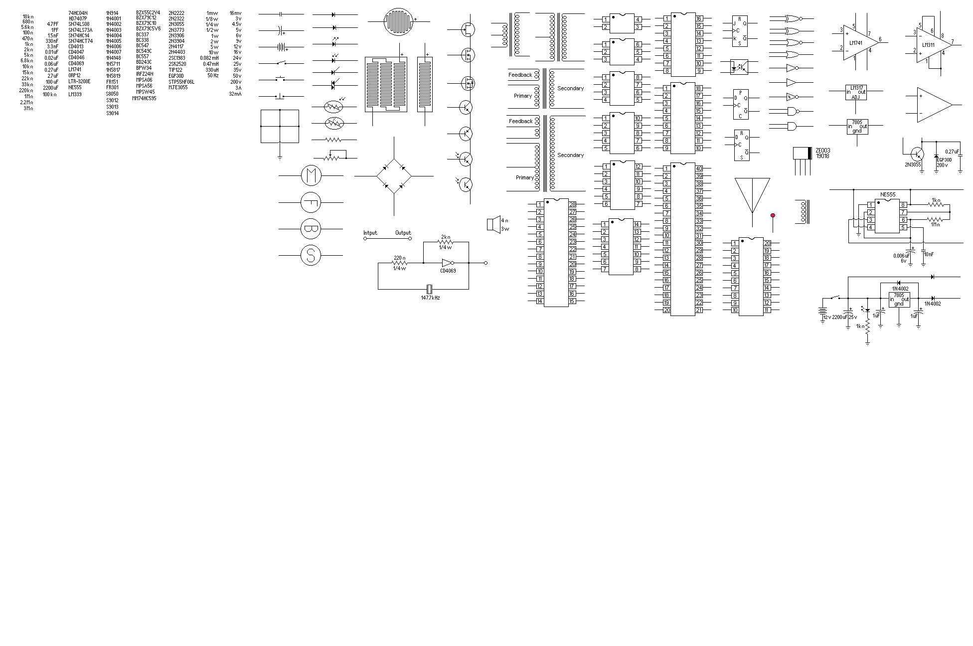
Once I have a working photo of the circuit board I open a paint schematic template I use to build my schematics in. It has the components I use the most, even a couple small basic circuits I use the most. All I have to do is copy and paste the components to my heart’s content.
Right after opening the template I Save As under the name of the new circuit name, “2.5 Watt AB Amplifier.” I do this so I don’t mess up the template for future use.
First Trace

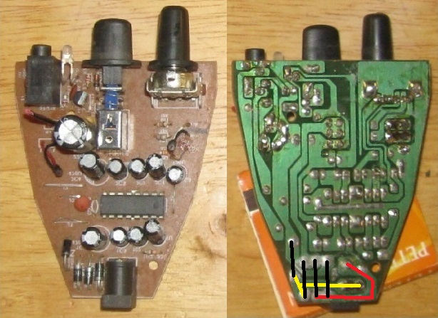
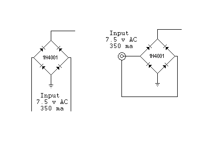
With this circuit I started at the power in and traced in paint the rectifier. Do not try to trace too much of the circuit board at one time or you can get lost in your tracings.
Remember rule number one, “A device is not one circuit, a device is a number of circuits put together to make a working device.”, so analyze the device one micro circuit at a time.
I Save As under a new name to keep my original, this way I have one image to go back and see what I have done in the past. And I have the original for making new tracings.
Then I open my amplifier template to make the rectifier schematic. At this point I decide if I want to include the female input jack or just the input voltage.
Then I save my work.
I don’t concentrate on using the same colors every time I trace, I just make sure I use different colors for different components and different conductors.
Downloads
Second Trace

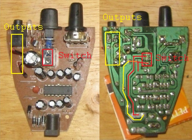
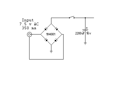
For the second trace I opened the original photo of the circuit board and traced to the switch and the power capacitor as well as made notes on the circuit board.
I saved this under a new file name and opened my amplifier template adding the two new components to my schematic.
Third Trace

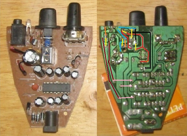
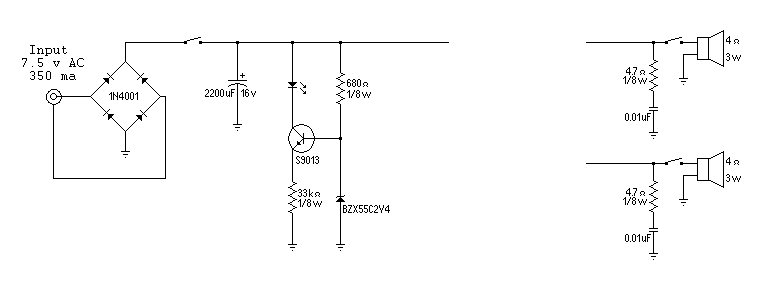
In the third tracing I opened the original circuit board pic and traced the output circuit, and the power on LED circuit. Then like in the other steps I saved under a new file name.
To make sure I used the right symbol for the power on LED’s transistor in the schematic, I looked up the transistors part number and retrieved its datasheet.
For the Zener diode I had to desolder it and remove it from the circuit board to read the part number and retrieve the datasheet.
Once I had the datasheets I added the new components to the schematic.
Fourth Tracing


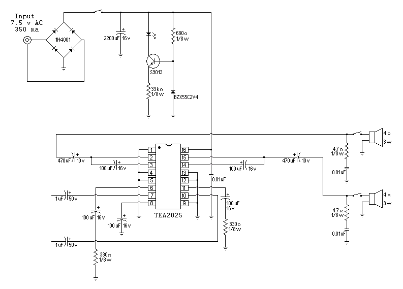
In the fourth tracing I looked up the datasheet for the IC first and compared the tracing to the datasheet as I traced to make sure I had the pins correct, and then I saved the pic under a new name.
This time I went from the pic, to the datasheet, to the schematic, bouncing between the three to make sure all the connections were correct in the schematic.
Downloads
Fifth Tracing

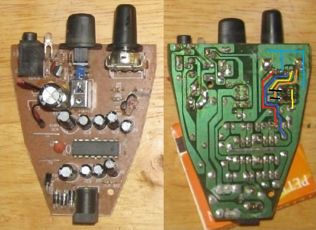
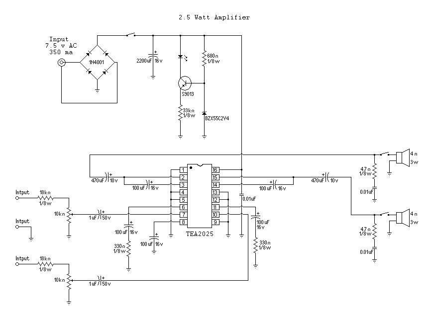
In the fifth tracing I traced the input of the amplifier and added the new components to the schematic.
And in just an hour and a bit I had a schematic of a 2 input 2.5 Watt Stereo Amplifier.
Unknown Component
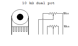
Although I was able to get the datasheets or read the codes on almost all the components there was one component that could have been a problem if I didn’t reverse engineer the circuit board. The volume control is marked 103 with 6 pins in a row telling me it is a 10 kΩ dual pot but not the pinouts.
Knowing audio in is at one side of the pot, ground is at the other side of the pot, and audio out is on the adjust I came up with this schematic for the pot.