Project 6: a Simple Communication System
by NAEastland in Circuits > Electronics
4505 Views, 7 Favorites, 0 Comments
Project 6: a Simple Communication System

In this project, you will design a 4-to-1 mux and a decoder with an enable signal as a “de-mux” to implement a simple serial data transmitter. Both mux and de-mux will be implemented in two Verilog files for future re-use. Another Verilog file will be used to wrap up the mux and de-mux to form a communication system. This hierarchical design methodology will help manage design complexity, promote design reuse, and allow parallel development.
What you need:
-Have the Xilinx® Vivado WebPACK™ installed.
-Have your FPGA board set up.
-Know how to write behavioral Verilog HDL code and write XDC files.
While all the basic theory will not be covered here, these links can provide you with the relevant background you will need:
Time Multipleximg Data Transmission
The word multiplexer has its origins in telecommunications, defining a system where one signal is used to transmit many different messages, either simultaneously or at different times. “Time-multiplexing” describes a system where different messages use the same physical signal, with different messages being sent at different times. A multiplexer can be used as a simple time multiplexer if the select inputs are used to define the time window and the data inputs are used as the data sources. A decoder with an enable can be used as a de-multiplexer.
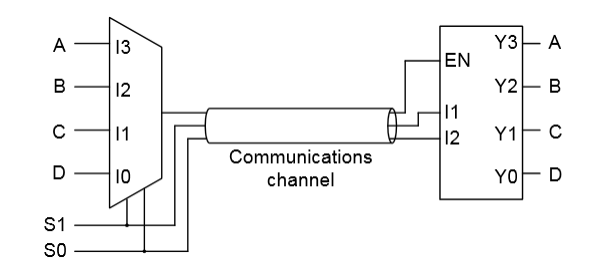
In the system diagram at the top, a 4-to-1 multiplexer selects one of four inputs to pass through to the output, and a de-multiplexer (decoder with enable signal) takes a single input and routes it to one of four outputs.
Implement a 4-to-1 Multiplexer
Create a project for your board, and new a Verilog Module named mux, with four data inputs (I0, I1, I2, I3), two select inputs (S1, S0), and a single output (Y).
1 module mux (
2 I0, I1, I2, I3, S0, S1, Y
3 );
4
5 input I0, I1, I2, I3, S0, S1;
6 output reg Y;
7
8 // Your behavioral description of Y
9 // using if-else or case statements
10
11 endmodule
Code the functionality of the mux behaviorally, as we discussed in the previous project.
Create a test bench to simulate the multiplexer and make sure it is working properly.
Implement a De-Multiplexer

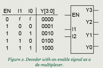
A de-multiplexer can be built using a binary decoder with an enable signal. The functional definition of a binary decoder with an enable signal is shown in Fig. 2 above.
In the same project, create a new Verilog Module named demux, with 3 inputs (En, I0, I1), and four outputs (Y0, Y1, Y2, Y3).
1 module demux (
2 En, I0, I1, Y0, Y1, Y2, Y3
3 );
4
5 input En, I0, I1;
6 output reg Y0, Y1, Y2, Y3;
7
8 // Your behavioral description of Y
9 // using if-else or case statements
10
11 endmodule
Code the functionality of the mux behaviorally, as we discussed in the previous project.
Create a test bench to simulate the de-multiplexer and make sure it is working properly.
Create a Wrapper As the Top Level Module

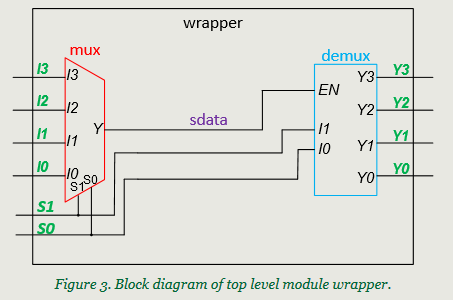
In this step we are going to create the top level module, in which a mux and a de-mux will be instantiated and connected properly to form a simple time multiplexing communication system. The system diagram is shown in Fig. 3 above.
In the block diagram, the input/output ports of the module wrapper is in green; the input/output ports of module mux and demux is displayed in black italic; and the internal wire of wrapper module is in purple.
In the project, create a new Verilog module file named wrapper with 4 data inputs (I3, I2, I1, I0), 2 select inputs (S1, S0), and four outputs (Y3, Y2, Y1, Y0).
1 module wrapper (
2 I0, I1, I2, I3, S0, S1, Y0, Y1, Y2, Y3
3 );
4
5 input I3, I2, I1, I0, S1, S0;
6 output Y0, Y1, Y2, Y3;
7
8 // Structural Description of wrapper
9
10 endmodule
Declare internal wire sdata after input and output declaration.
1 wire sdata;
Instantiate the de-mux (named output_demux) and connecting wires in wrapper to the I/O ports of the de-mux.
1 demux output_demux (
2 .En(sdata),
3 .I1(S1),
4 .I0(S0),
5 .Y0(Y0),
6 .Y1(Y1),
7 .Y2(Y2),
8 .Y3(Y3)
9 );
Put everything together. The top level Verilog module will be as follows:
1 module wrapper (
2 I0, I1, I2, I3, S0, S1, Y0, Y1, Y2, Y3
3 );
4
5 input I3, I2, I1, I0, S1, S0;
6 output Y0, Y1, Y2, Y3;
7
8 // Structural Description of wrapper
9 wire sdata;
10
11 mux input_mux (
12 .I3(I3),
13 .I2(I2),
14 .I1(I1),
15 .I0(I0),
16 .S1(S1),
17 .S0(S0),
18 .Y(sdata)
19 );
20
21 demux output_demux (
22 .En(sdata),
23 .I1(S1),
24 .I0(S0),
25 .Y0(Y0),
26 .Y1(Y1),
27 .Y2(Y2),
28 .Y3(Y3)
29 );
30
31 endmodule
Create a XDC file as follows:
-I3 to SW3; I2 to SW2, I1 to SW1, I0 to SW0
-Y3 to LED3; Y2 to LED2, Y1 to LED1, Y0 to LED0
-S1 to BTN1, S0 to BTN0