Project 1.2: Use Switches to Control LEDs
by Commanderfranz in Circuits > Electronics
23391 Views, 22 Favorites, 0 Comments
Project 1.2: Use Switches to Control LEDs

This project demonstrates how to use Verilog HDL with an FPGA board. In this project you will use a switch on your FPGA board to turn on an LED. In doing this, you will learn the first steps of writing Verilog code and observe how a switch can control LEDs on an FPGA board. You won't need to have a really thorough understanding of digital engineering to make this project work; however, if you would like to know the inner workings of the digital circuit, more information is available in Project 1.1.
What you need:
- Have already completed Project 1.1.
I will not cover all the basic theory necessary in this tutorial, but If you are interested, you can follow these links:
Background Knowledge

A digital circuit contains a power supply, devices, and conduction nets. Some nets provide the circuit with inputs from the “outside world,” while others, conversely, provide information from the circuit to the outside world. The nets that provide an interface between the circuit and the outside world are called ports.
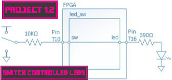
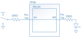
Circuits need input devices to generate input signals. Input devices can take many forms, among them keyboards (such as on a PC), buttons, and switches. Circuits also need output devices to communicate their state to the user. In this project, a switch is used as the input device and an LED is used as the output device. The digital circuit we will build is called the “led_sw,” as shown in Fig. 1 below. The circuit created in this project will be implemented inside the FPGA board. The board has an input port called “sw,” which receives an input signal from the external switch in the circuit and an output port called “led,” which drives the external LED in the circuit. The “led_sw” is a simple circuit that bypasses the signal on the input port and directly sends information to the output port. You can view this as a direct wired connection between the net “sw” and the net “led.” The circuit will be implemented using Verilog HDL. On different FPGA boards, switches and LEDs are connected to different pins on an FPGA chip. Thus, a user constraint file (XDC) is needed to map the input and output net of the circuit to the physical pin location on the FPGA chip. Take Nexys3 as an example, the Slide Switch 0 (SW0) is connected to FPGA pin T10, and FPGA pin U16 drives LED 0 (LD0). When you slide the switch to the ON position, a high voltage will be placed on FPGA pin T10, which is mapped to the input port of the circuit “led_sw.” The digital circuit then transmits the signal onto the output port LED, which is connected to FPGA pin U16. The high voltage on the output port “led” will cause a voltage drop between node A and node B. This voltage drop will drive current through the LED, which will light the LED and inform the user that the switch is on.
Create a New Project

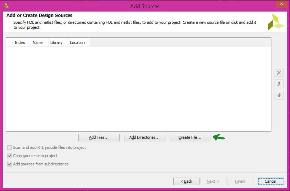
Create a Verilog module (.v) as explained in the previous project and name it “led_sw”. Follow the same steps as adding the existing .v file, except instead of pressing add file press create file. Add sources-> add or create design sources -> create file. Then hit finish.
Create Inputs and Outputs
Once you have created the module, an inputs and outputs setting page will appear.Add “sw” as an input; ignore the “bus,” “MSB,” and “LSB.” Then add “led” as an output; ignore the “bus,” “MSB,” and “LSB.”
Template
In step 1, a template has been generated by the Xilinx tools as follows:
1 module led_sw(
2 output led,
3 input sw
4 );
In this code, you have demonstrated that the net “led” is the output and the “sw” is an input.
Assign Statement
Now it is time to implement the circuit. At this time we will use an “assign” statement in Verilog to connect the output port “led” to the input port “sw”. The “assign” statement is used so that whenever a signal is placed on the input net it will be transmitted directly to the output port.
1 assign led = sw;
2
Final Module
Lastly, you must always make sure to end the module with the “endmodule” code. When you have completed this project file, it should look like this:
1 'timescale 1ns/1ps
2 module led_sw(
3 output led,
4 input sw
5 );
6
7 assign led = sw;
8
9 endmodule
10
Create XDC File
The circuit has been implemented but the Xilinx tools still need to know what physical pins on the FPGA the input and output ports are mapped to. The XDC file will give the tools for this information. Please choose your board in the drop-down menu to see the XDC file corresponding to your board, as pin locations of LD0 and SW0 vary from board to board.
1 set_property PACKAGE_PIN U9 [get_ports {sw}]
2 set_property IOSTANDARD LVCMOS33 [get_ports {sw}]
3 set_property PACKAGE_PIN T8 [get_ports {led}]
4 set_property IOSTANDARD LVCMOS33 [get_ports {led}]
You can find the location you need from the schematic of your FPGA board, or you can download the master XDC for your board from the Digilent website and copy the corresponding lines for this step.
Remember that the XDC file connects the signal you described in your .v file to the physical pin on the board. If the signal is named sw in the .v file, then the physical pin must be named sw in the .xdc file.
Generate Bitstream and Program
Click on “Generate Bitstream" to generate the bit file and download it to your FPGA board. After you program your board, you can slide on the SW0 on your board to turn on LD0.
Test Your Knowledge
Now that you've completed this project, try these modifications:
In this project, we used only one switch to control one LED. You can modify the code a little bit and use all 16 switches on your board to control the 16 LEDs. To do so, you would assign SW0 to control LD0, SW1 to control LD1, and so on. Try doing this with and without using busses. Bus notation is similar to that of array notation in C.
Now think of a way to modify your project a little bit to change which switch controls which LED. For example, make SW0 control LD6.