Portable Function Generator on WiFi and Android
by Faransky in Circuits > Tools
1818 Views, 4 Favorites, 0 Comments
Portable Function Generator on WiFi and Android


Near the end of 20th century, various technological innovations popped up, especially in the field of communications; but not only. For us, users, consumers and engineers came to light rapid developing of electronic devices, that can make our lives a lot easier: Smart watches, smart homes, smartphones etc.
Since everything can be "smart" nowadays, I've decided to design a super-useful device to be the part of essential electronic lab equipment - Portable Function Generator, controllable by Android OS based smartphone via WiFi direct or WiFi Local Area Network (WLAN).
Why should we build this device?
A vast majority of testing equipment is pretty much expensive nowadays. And sometimes, these devices aren't portable. As a solution for high prices, lack of portability and lack of device network access, device provides dual channel waveform generator, that is indeed portable and has an unrestricted access to the network - either internet or local one.
And of course, device should be built because of enthusiasm, obeying the DIY principles - Sometimes we just have to do things ourselves in order to feel right :)
Key Features
Power Supply
- USB Type-A connector, for both power supply systems and programming
- Complete Li-Ion battery management system - Charging and stable modes
- Smart Switch implementation - no need for power toggling switch
- Dual power supply: +3.3V and -3.3V for symmetrical voltage waveform generation
Waveform Generation
- Implementation of DC level at the output cascade - biased waveform between the voltage boundaries
- DDS based 4-type waveform generation - Sine, triangle, square and DC
- Up to 10MHz frequency support
- Output current up to 80mA with 500mW maximum power availability
- Separated channels for waveform generation - split AD9834 based circuits
Communication
- Implementation of ESP32 - Applicable WiFi capabilities
- Complete TCP/IP support by generator device and Android smartphone
- Ability to store user parameters for every device cycle
- State monitoring - both systems are aware of each other state: FuncGen (let's call it this way from now on) and smartphone.
User Interface
- 20 x 4 Character LCD with simple 4-bit data interface
- Android application - complete user control over the FuncGen device
- Buzzer circuit - sound feedback to user
Block Diagram - Hardware


Microcontroller Unit - ATMEGA32L
Microcontroller is a programmable chip that consists of all the computer functionality that resides in a single electronic chip. In our case, it is the "brain" and a central component of the system. The purpose of the MCU is to manage all the peripheral systems, handle communication between these systems, controlling hardware operation and providing complete support for user interface and its interaction with an actual user. This project based on ATMEGA32L MCU, that may operate on 3.3V and a frequency of 8MHz.
Communication SoC - ESP32
This SoC (System on Chip) provides complete communication support for FuncGen - Access to WiFi capabilities including direct, local or internet communication. Purposes of device are:
- Handling data transmission between Android app and FuncGen device
- Management of control/data messages
- Support of continuous TCP/IP Client-Server configuration
In our project the SoC is espressif ESP32, that is too popular to expand on it even further :)
Li-Ion Battery Management System
In order to transform our device into portable one, device contains designed Li-Ion battery charging circuit. Circuit is based on MC73831 IC, with controllable charging current via adjusting the value of a single programming resistor (We'll cover this topic in Schematics step). Device power supply input is USB Type-A connector.
Smart Switch Circuit
Smart switch device power control circuit provides complete software control over device shutdown sequence and lack of need for external toggle switch for device battery voltage cutoff. All the power operations are done by pressing push button and MCU's software. In some cases, there would be need to shut the system down: Low battery voltage, high input voltage, communication error and so on. Smart switch is based upon STM6601 smart switch IC, that is cheap and very friendly to play around with.
Main Power Supply Unit
This unit consists of two battery-driven power supply circuits - +3.3V for all the digital / analog supply circuits and -3.3V for FunGen symmetrical output relative to 0V potential (i.e generated waveform can be set in [-3.3V:3.3V] region.
- Main supply circuit is based on LP3875-3.3 LDO (low dropout) 1A linear voltage regulator.
- Secondary supply circuit is based on LM2262MX IC, that performs DC-DC negative voltage conversion via capacitor-charge-pump - system that IC is based on.
Waveform Generators System
System was designed with emphasis on separate DDS (direct digital synthesis) integrated circuits, that allow complete waveform generation control by MCU's SPI (serial peripheral interface). The circuits that were used in design are Analog Devices AD9834 that may provide different types of waveforms. The challenges we need to face while working with AD9834 are:
- Fixed waveform amplitude: Waveform amplitude is controlled by external DAC module
- No regard for offset DC level: Implementation of summing circuits with desired DC offset values
- Separate outputs for square wave and triangle/sine wave: Implementation of high frequency switching circuit thus each channel single output can provide all of the desired waveforma: sine, triangle, square and DC.
Liquid Crystal Display
LCD is a part of UI (user interface), and its purpose is to allow user to understand what device does in real time mode. It interacts with user at every device state.
Buzzer
Simple tone generator circuit for additional feedback from device to user.
Integrated ISP Programmer
There is a persisting problem for every engineer when it comes to programming process: There is always that worst need to disassemble the product in order to reprogram it with a new firmware. To overcome this inconvenience, AVR ISP programmer was attached to device from the inside, whereas USB data and power lines are tied to device' USB Type-A connector. In this configuration, we just need to plug our FuncGen via USB cable for either programming or charging!
Block Diagram - Networking

Dual Channel Function Generator
Main device. The one we've reviewed in the previous step
ESP-WROOM-32
Integrated System-on-Chip with WiFi and BLE capabilities. SoC is attached to the main board (We'll cover this in schematics step) via UART module and acts as a message transciever between main device and Android smartphone.
WiFi Local Network
Smartphone and device will communicate via WiFi direct or local area network, based on TCP server/client configuration. When devices recognize each other on the WiFi, main device creates TCP server with appropriate parameters and is able to send/receive messages. Device acts as a secondary to the smartphone. Android device on the other hand, connects to TCP server as a client network device, but is regarded as primary message transmitter - smartphone is the one who initiates complete communication cycle: Sending message - receiving reply.
Android Smartphone
Android OS based smartphone device that runs on FuncGen application
Parts, Tools, IDE and Bill of Materials


Bill Of Materials (See attached XLS table)
UI And System Connections
- 1 x 2004A Char-LCD 20x4 Blue
- 1 x USB Type B Connector
- 1 x 10 Set Mini Micro JST XH 2.54mm 4 Pin
- 1 x 6pcs Momentary SW
PCB Ordering (According to Seeed Studio)
Base Material FR-4
No. of Layers 2 layers
PCB Quantity 10
No. of Different Designs 1
PCB Thickness 1.6mm
PCB Color Blue
Surface Finish HASL
Minimum Solder Mask Dam 0.4mm↑
Copper Weight 1oz
Minimum Drill Hole Size 0.3mm
Trace Width / Spacing 6/6 mil
Plated Half-holes / Castellated Holes No
Impedance Control No
Tools
- Hot glue gun
- Tweezers
- Cutter
- ~22AWG wire for the malfunction handling purposes
- Soldering iron/station
- Soldering tin
- SMD rework station (optional)
- 3D printer (Optional)
- Extruding file
- AVR ISP Programmer
- USB to Serial Converter (Optional, for debugging purposes)
Integrated Development Environment (IDE) and Software
- Autodesk EAGLE or Cadence Schematic Editor / Allegro PCB Editor
- OpenSCAD (Optional)
- Ultimaker Cura (Optional)
- Saleae Logic (For troubleshooting)
- Atmel Studio 6.3 or above
- Android Studio or Eclipse IDE
- Docklight Serial Monitor / Other COM port monitoring software
- ProgISP for AVR ATMEGA32L flash programming
Downloads
Hardware Design - Main Board


Battery Management Circuit
Battery charging circuit is based on MCP7383 IC, that allows us to select a desired charging current for Li-Ion battery - 3.7V with capacity of 850mAh. Charging current is set by programming resistor value (R1) in our case
R1 = 3KOhm, I(charge) = 400mA
USB voltage VBUS is filtered by π-filter (C1, L3, C3) and acts as a power source for charging circuit.
Voltage divider circuit (R2, R3) allows MCU to indicate whether external USB power supply is connected or not, by providing following voltage to MCU A/D channel:
V(indication) ~ (2/3)V(BUS)
Since our A/D of ATMEGA32L is 12-bit, we can calculate the digital range:
A/D(range) = 4095V(indication) / V(REF).
A/D ∈ [14AH : FFFH]
Smart Switch Power Unit
Circuit allows system to control power supply to every designed block both from push-button and software on MCU and is based on STM6601 Smart-Switch with POWER option instead of RESET. The terminals that we want to consider are these:
- PSHOLD - Input line, that defines device state: if is pulled LOW, device disables all the secondary power supply units (+3.3V and -3.3V). If held HIGH - device maintains ON state.
- nSR and nPB - Input lines. Push button terminals. When falling edge is detected on these pins, device tries to enter power up / down mode
- nINT - Output line. Pulled LOW every time when push button is pressed
- EN - Output line, is used as power enable for the secondary power supply units. While is held LOW, both secondary power supplies are disabled
There are some important notes before we proceed to the final design:
- PSHOLD should be pulled-up to 3.3V, because there are cases when MCUs are forcing all the I/Os to be in HIGH-Z state. In this case, state of PSHOLD from the MCU is unknown and may dramatically affect device programming process.
- STM6601 should be ordered with an EN adjusting option on long press, instead of RESET option (I've fallen in that one).
Power Supply Unit: +3.3V
Main power supply for all the systems in our project. When the +3.3V line is held at GND level (i.e. No voltage presents), all the IC except smart switch are disabled. The circuit is based upon LDO LP-3875-3.3 IC, with a capability of being controlled via EN terminal and provide current up to 1A.
The power source for this circuit is the battery voltage, with attached A/D indicator for sensing VBAT in configuration, similar to VBUS sensing circuit. In this case, the calculations slightly differ;
V(Battery-to-A/D) = 0.59V(Battery); A/D(range) ∈ [000H : C03H]
Power Supply Unit: -3.3V
Negative voltage supply circuit allows us to generate symmetrical waveforms with a DC factor of 0V (i.e. The waveform average value is able to be 0V). This circuit is based on LM2662MX IC - DC/DC converter that operates on a "charge pump" method. Maximum output current of the circuit is 200mA which is sufficient for our design requirements - we are limited with 80mA output current from each device' channel.
IC performs all the needed work, so only parts we need to attach are two electrolytic capacitors: C33 for switching and C34 for -3.3V line bypass (noise reduction considerations). The frequency of the switching is negligible in design if we are placing the circuit far enough from waveform generation parts (We'll discuss it at PCB Layout step).
Microcontroller Unit - MCU
This is the manager and the CEO of our system - control, network handling, message transmission and UI support - everything is by MCU.
The MCU that was chosen is Atmel ATMEGA32L, where L stands for supported voltage operation ∈ [2.7V : 5.5V]. In our case, the operating voltage is +3.3V.
Let's consider the main operation blocks, that are necessary to understand, working with MCU in our design:
- External Oscillator - Is an optional component, since we are interested in 8MHz operating frequency
- Peripheral Control, SPI Network - All the peripheral devices (excluding ESP32) are communicating with MCU via SPI. There are three shared lines for all devices (SCK, MOSI, MISO) and every peripheral circuit has its dedicated CS (Chip Select) line. The SPI devices that are a part of device:
- D/A for amplitude control - Channel A
- D/A for amplitude control - Channel B
- AD9834 device - Channel A
- AD9834 device - Channel B
- D/A for bias voltage control - Channel A
- D/A for bias voltage control - Channel B
- Digital Potentiometer for LCD brightness/contrast settings
- LCD Support - Since LCD is a generic 20 x 4 character display, we are using 4-bit interface (Lines D7:D4), control pins (Lines RS, E) and brightness/contrast control (Lines V0 and Anode)
- RGB LED support - This module is optional, but there is common cathode RGB LED connector with appropriate resistors, connected to the MCU.
- Power Control - MCU performs power system monitoring in the real time mode, and handles all the needed power events:
- VBAT_ADC - Battery voltage monitoring and determining its state (ADC0 Channel)
- PWR_IND - Indication of external power supply connection (ADC1 Channel)
- PS_HOLD - Primary power enable line for all of the defined systems. When is pulled low by the MCU, device is powered down
- Interrupt terminal of smart switch - Push button state monitoring
- WiFi Network Management - ESP32: MCU communicates with ESP32 via UART interface. Since 8MHz allows us to implement baud rate of 115200 with a relatively small error, we can use ESP32 in the circuit without pre-definitions of baud rate changes.
AVR ISP Programmer
Our MCU is programmed via SPI with resetting line (/RST) has to be pulled HIGH for a proper operation (if not - MCU will find himself in a reset state forever).
In order to allow device to be both programmed and charged via USB, I've attached AVR ISP programmer (Small-sized product, bought from eBay). In order to maintain device complete USB support, there is need to tie USB Type-A (D+,D-,VBUS and GND) terminals with AVR ISP device.
Waveform Generation Circuit
The core of device is these circuits. AD9834 is a low-power DDS device that provides us all of the waveforms we would like to retrieve from the system. Circuits contain two independent AD9834 ICs with separated external 50MHz oscillators (as it can be seen in the schematics). The reason for separated oscillator is a digital circuits noise reduction considerations, so the decision was to handle proper 50MHz lines with oscillators placed adjacent to AD9834.
Now let's look at some math:
Since DDS device operates on Phase Wheel technology with output value held in a 28-bit register, we can describe waveform generation mathematically:
dP(phase) = ωdt; ω = P' = 2πf; f(AD9834) = ΔP * f(clk) / 2^28; ΔP ∈ [0: 2^28 - 1]
And according to AD9834 datasheet, taking in account maximum frequency, output frequency resolution may be obtained:
Δf = k * f(oscillator) / f(maximum) = 0.28 * 50M / 28M = 0.187[Hz]
AD9834 ICs provide an analog current output for triangle/sine wave (IOUT terminal) and digital output for square wave (SIGN_OUT terminal). The usage of sign bit is a little bit tricky but we are able to handle it - Each time DDS passes the threshold of comparison value, SIGN_OUT behaves accordingly. A 200Ohm resistor is attached to each channel's output, so the output voltage would have a meaningful values:
I(single channel) = V(output) / R(voltage selection); V(output) = R(VS)*I(SS) = 200I(SS) [A]
Amplitude Control (D/A) Circuits
According to datasheet of AD9834, its amplitude may be adjusted by providing current to the DDS full scale system, so with the help of dual D/A IC, we can control the output signal amplitude by adjusting that current. Once again, some math:
I(full scale) = 18 * (V_REF - V_DAC) / R_SET [A]
According to schematics and putting some numbers to equation:
I(full scale) = 3.86 - 1.17 * V_DAC [A]
D/A module used in design is 12-bit MCP4922, when the current is in the range of [0mA : 3.86mA] and linear amplitude function is:
V(amplitude select) = 1 - [V(D/A) / (2^12 - 1)]
Waveform Multiplexing Circuit
Square wave and sine/triangle wave generation outputs are separated at AD9834 hence we have to use a high speed multiplexing circuit for both outputs in order to allow retrieving all desired waveforms from a single separated channel. The multiplexer IC is an ADG836L analog switch with a very low on-resistance (~0.5Ohm).
The selection table that MCU is using for the outputs as it is:
Mode Selection [D2:D1] | Output Channel A | Output Channel B
   	00             |  Sine/Triangle	  |  Sine/Triangle
	01             |  Sine/Triangle	  |     Square
	10             |     Square	  |  Sine/Triangle
	11             |     Square	  |     Square
Bias Voltage Control (D/A) circuits
One of waveform generator's main features is to control its DC value. In this design it is done by setting desired D/A voltage per each channel, and these bias voltages are summed with multiplexed outputs that we have discussed a little bit earlier.
Voltage retrieved from D/A lies in the range [0V : +3.3V] so there is an op-amp based circuit that maps the D/A range to [-3.3V : +3.3V], allowing device to provide full range of desired DC component. We will skip the annoying analytical math, and just focus on the final results:
V_OUT(channel B) = V_BIAS_B(+) - V_BIAS_B(-); V_OUT(channel A) = V_BIAS_A(+) - V_BIAS_A(-)
Now, the DC component range located in range [-3.3V : +3.3V].
Summing Circuits - DC Components and Waveform Outputs
At this point we have everything we need for the proper device output - Bias Voltage (DC component) in the full voltage range, and multiplexed AD9834 outputs. We'll make that happen by using the summing amplifier - op-amp configuration
Let's skip math once again (We've covered a lot of mathematical approach already) and write down the final result of the summing amplifier's output:
V(device output) = V(positive bias) - V(negative bias) - V(multiplexed output) [V]
Hence:
V_OUT = ΔV_BIAS - V_AD9834 [V]
Output connectors of BNC type are connected with a selection resistors (R54,R55; R56, R57). The reason for that is that in the case that design may be dysfunctional, we still can select if we would like to use summing amplifier.
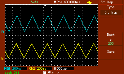
Important Note: The resistor networks of the final summing amplifiers can be adjusted by a designer, in order to change maximum amplitude that can be retrieved from device. In my case, all the amps share the same gain = 1, thus the maximum buffered amplitude is 0.7Vpp for triangle/sine wave and 3.3Vpp for square wave. The specific mathematical approach can be found among step's attached images.
ESP32 As External Module
MCU communicates with ESP32 via UART interface. Since I wanted my own PCB for the ESP32, there are 4 terminals available to connect: VCC, RX, TX, GND. J7 is a interface connector between PCBs, and ESP32 will be allocated as external module inside the device.
User Interface - LCD and Speaker
LCD that was used is a generic 20 x 4 character display with a 4-bit interface, As it can be seen from the design there is a SPI digital potentiometer attached to LCD terminals "A" and "V0" - its purpose is to adjust brightness and contrast of LCD module programmatically.
Speaker provides sound output for the user by simple square wave generation from the MCU. The BJT T1 controls the current through the speaker that can be just in two states - ON / OFF.
Downloads
Hardware Design - ESP32 Module
.bmp)
ESP32 is used as an external module for main PCB. Device communication is based on AT commands, that are available on a generic device' firmware.
There is not much to expand on this design, but there are some notes for design:
- For the failure handling of using proper UART module of ESP32, I've attached three selection resistors for both TX and RX lines. (0Ohm for each). For standard configuration, UART2 module is used for AT commands (R4, R7 must be soldered)
- Device has 4-line output - VCC, GND, TX, RX.
- IO0 and EN pins evaluate device operation and should be designed as it is provided in the schematics
All the PCB features we'll cover in the following step.
PCB Layout


The goals of designing a PCB
- Create embedded system for all the integrated circuits on the same board
- Improve device performance via designing a single main PCB
- Cost reduction - if you would like to look up the prices, low-cost designs are REALLY low cost
- Minimize the electronic board size
- Easy to troubleshoot - We can use TPs (Test points) for each possible malfunctioning line.
Technical Parameters
Both PCBs: main and ESP32 board share the same characteristics for the manufacturing process - low cost and operable for our purposes. Let's see them:
A - Main Board
- Size: 10cm x 5.8cm
- Number of Layers: 2
- PCB thickness : 1.6mm
- Minimum trace space/width: 6/6mil
- Minimum via hole diameter: 0.3mm
- Copper to the edge of PCB minimum distance: 20mil
- Surface finishing: HASL (Pretty good looking silver color cheap type)
B - Main Board
- Size: 3cm x 4cm
- Number of Layers: 2
- PCB thickness : 1.6mm
- Minimum trace space/width: 6/6mil
- Minimum via hole diameter: 0.3mm
- Copper to the edge of PCB minimum distance: 20mil
- Surface finishing: HASL
3D Enclosure

I didn't design it by myself, because at the time I was persuading this device to work, so I wasn't aware of all the 3D printing basics at all. Thus I've used a SCAD project from Thingiverse, and attached different apertures to the boundaries, according to my device' specifications.
- Printing Device: Creality Ender-3
- Bed Type: Glass, 5mm thickness
- Filament Diameter: 1.75mm
- Filament type: PLA+
- Nozzle Diameter: 0.4mm
- Initial Speed: 20mm/Sec
- Average Speed: 65mm/Sec
- Support: N/A
- Infill: 25%
- Temperature:
- Bed: 60(oC)
- Nozzle: 215(oC)
- Filament Color: Black
- Total Number of Apertures: 5
- Number of Enclosure Panels: 4
- TOP Shell
- Bottom Shell
- Front Panel
- Back Panel
Software Implementation - MCU


GitHub Link to Android and Atmega32 Code
Software Algorithm
All the operations that are performed by the MCU, are described in attached flowcharts. In addition to that, there is an attached code for the project. Let's cover software specifications:
Power-up
At this stage, MCU performs all the initialization sequences along with determination of stored communication type with Android device: Direct WiFi or WLAN network communication - this data is stored in EEPROM. User can redefine Android device pairing type at this stage.
Direct Android Device Pairing
This type of pairing is based on WiFi network creation by the FuncGen device. It will create AP (Access Point) and a TCP server on a local device IP with a specific SSID (WiFi network name) and a specific port number. Device should hold the state - open for connections.
When Android device is connected to FuncGen, MCU enters ACTIVE mode, and responds according to user instructions from the Android device.
WLAN Pairing
In order to communicate on a local WiFi network, MCU should provide commands for the ESP32 to create AP, communicate with Android device and exchange the crucial network data:
- Android device receives from FuncGen its MAC address, stores it in memory.
- FuncGen device receives form Android device selected WLAN parameters: SSID, type of security and Password and stores it in EEPROM.
When devices are indeed connected to the same WLAN, Android device will search for the FuncGen by scanning all the MAC addresses of devices, connected to the WLAN. When Android device determines MAC match, it tries to communicate.
Connection and State Handling - MCU
When devices communicate with each other, the protocol (See pre-final step) stays the same, and the flowchart is the same.
Device State Monitoring
Timed interrupt provides to MCU necessary details for state handling. Each cycle of timer interrupt, the following list of parameters are updated:
- External power supply - On/Off
- Battery voltage state
- UI update for each customization
- Push-Button: Pressed/Not Pressed
Software Implementation - Android App


Android app is written in Java-Android style. I will try to explain it in the same manner as the previous steps - by dividing the algorithm into separate code blocks.
Power Up Sequence
First sequence of the device. Here app logo is presented along with enabling GPS and WiFi modules of Android device (Don't worry, the GPS is needed for WiFi proper networks scan only).
Main Menu
After the app is booted, four buttons will appear on the screen. Buttons action:
- DIRECT CONNECTION: Initializing connection to FuncGen's AP by the SSID of IOT_FUNCGEN. If the connection is successful, device enters in main UI mode.
- WIFI CONNECTION: Device checks if there are stored data parameters in memory: wifi.txt, mac.txt. If there is no data stored, device will reject user request and provide pop-up message that WLAN pairing has to be done first.
- PAIRING: Communicating with FuncGen in the same way as DIRECT CONNECTION, but instead of continuous message exchange, there is a single handshake. Android device checks if it is already connected to the WiFi network, and request for user to enter password. If reconnection is successful, Android device stores SSID and passkey in wifi.txt file. After successful communication with FuncGen, it stores received MAC address in mac.txt file.
- Exit: Enough said :)
WiFi Scanning Manager
I wanted the application to be all-operational and without off-app adjustments to be made. So, I've designed WiFi Scanner, that performs all the needed operations to connect to the WiFi network with a known passkey and SSID.
Data Transmission and TCP Communication
This is the main code block in the app. For all the UI units there is a defined message in a specific format (Pre-final step), that force FuncGen to provide desired output for the channels. There are three types of UI fields in activity:
- Seek Bars: Here we define real-range of FuncGen output parameters
- Amplitude
- DC Offset
- LCD Brightness
- LCD Contrast
- Text Edit: In order to keep integer values well-defined and precise, frequency input is done via numbers only text boxes
- Buttons: Selection of parameters from the available lists:
- Waveform Type
- Sine
- Triangle
- DC
- Square
- OFF
- Get Info
- Battery Status (Percentage)
- AC Status (External Power Supply)
- Boot Option (For FuncGen MCU)
- Factory Setting
- Restart
- Shutdown
- Direct - Restart with direct pairing mode
- WLAN - Restart with WLAN pairing mode
- Exit to Main Menu: Enough Said :)
- Waveform Type
Testing
.BMP)