Panelizing PCBs for Seeed Using Eagle Free / Light
by spaceagerobotics in Circuits > Electronics
66666 Views, 42 Favorites, 0 Comments
Panelizing PCBs for Seeed Using Eagle Free / Light
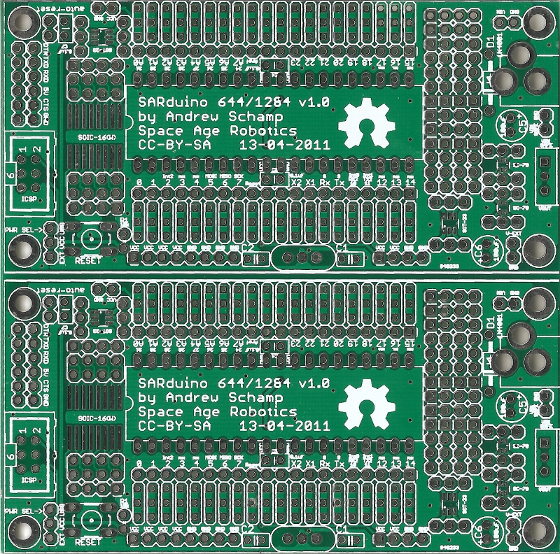

Some PCB fab houses (like SeeedStudio, with their Fusion PCB service) will allow you to panelize smaller PCBs. For example, if you have a 2.5cm x 5cm board, you could panelize two of them on to a single 5mm x 5mm PCB. Or, put a 7cm x 7cm board and a bunch of 3cm x 3cm boards onto a 10cm x 10cm panel. Seeed will allow up to 5 sub-boards on a panel.
The freeware and light versions of Cadsoft Eagle limit the design area of the PCB to 10cm x 8cm. This is enough to do many projects, but when you want to try and panelize to fill a 10cm x 10 cm board, it won't work. Plus, maintaining separate projects and updating them on the panel, and maintaining consistency of labels and reference designators can be a pain.
In this Instructable, I will show you an easy way to merge Gerber files generated from Eagle (or any other EDA tool) in a way that Seeed Studio will accept them for panelizing with their Fusion PCB service. I will be using the SARduino644 v1.0 board shown below as an example.
Design Board and Render Gerbers
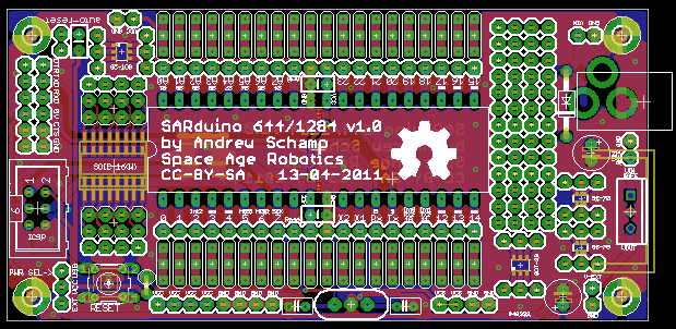
This has been covered elsewhere. Sparkfun has a set of particularly good tutorials. Note that Seeed requests that you put your order number on the silkscreen layer somewhere, so you might want to consider placing your order before going through the render/check cycle.
When you're happy with your board, and it passes Seeed's design rules, use the Seeed CAM processor to generate the Gerbers for your PCB.
When you're done, you should end up with the following files:
<board>.GTO - top silkscreen
<board>.GTS - top soldermask
<board>.GTL - top copper
<board>.GBO - bottom silkscreen
<board>.GBS - bottom soldermask
<board>.GBL - bottom copper
<board>.TXT - Excellon drill file.
Before you proceed, you should check the Gerbers carefully to make sure everything looks right *before* combining them into a panel, this will save time later if you find a problem. I like to use the online gerber viewer provided by CircuitPeople. You can make a zip of all the files and upload them in one go, and they will all be rendered to image files.
Install Gerbmerge and Patch for Seeed
Rugged Circuits has created an excellent program for merging gerber files, called, not unexpectedly, gerbmerge. This program will merge gerber files onto a panel with a layout you can specify.
Go download the latest version (currently 1.8) and install it.
In order to accept panelized PCBs, Seeed requires an outline for the entire panel to be present on all layers, otherwise, they will offer to change your order for multiple, separate boards, which defeats the entire purpose. Out of the box, v1.8 of gerbmerge does not support rendering the outline of the entire panel to all layers. However, I have successfully patched it to include this support. I have submitted this patch to the folks at Rugged Circuits, and they are considering including it in the next release. Until then, you'll have to apply it manually. But it isn't hard...
The latest patched version is in this gerberge-patched github repo. To patch your installation, find the installed files (for example, look for a gerbmerge folder in C:\Python<version>\Lib\site-packages\ on Windows, or in /usr/lib/python<version>/site-packages on Linux). Then apply these patches: https://github.com/space-age-robotics/gerbmerge-patched/commit/5078c7b33439912c465fb33fc0082b82cfac3687#diff-0 to the config.py and gerbmerge.py files.
If you're worried about messing up your installation, feel free to make a backup copy of the gerbmerge folder before you proceed. You might also consider setting up your merge configuration and layout first, and then adding the patch once you have it producing the output you want, so you have more confidence in the output.
Define Your Panel Configuration

The panel configuration file defines the source gerber files for each PCB, and specifies the details of the merged gerber output. Here is an explanation of some values you may want, from the SARduino644 panel configuration, which you can find in full here: https://github.com/space-age-robotics/SARduino/blob/master/panel.cfg
# I always use the local directory to contain all input gerbers, config files, and output files
projdir = .
# MergeOut is the prefix of the output files.
MergeOut = merge2
# CutlineLayers will determine where the subboard markings are, which will help in separating them. These are the accentuated lines between the two instances of the board in the image below.
CutLineLayers = *topsilkscreen,*bottomsilkscreen
# OutlineLayers is used by the patched gerbmerge, it defines which layers the entire panel outline will be drawn on. Seeed requires this on all layers.
OutlineLayers = *toplayer,*bottomlayer,*topsilkscreen,*bottomsilkscreen,*topsoldermask,*bottomsoldermask
# here you can specify the maximum dimensions allowed by the Seeed PCB service you ordered (in inches).
# gerbmerge will warn you if your final panel (based on your layout) exceeds these dimensions.
PanelWidth = 3.93
PanelHeight = 3.93
# comment out the margins or set them to zero if you want the maximum amount of useable area on your panel.
#LeftMargin = 0.1
#RightMargin = 0.1
#TopMargin = 0.1
#BottomMargin = 0.1
# spacing determines how much space between the panels. I found 0.0625 to be plenty of space for a band-saw blade, I may reduce it a hair in the next run.
XSpacing = 0.0625
YSpacing = 0.0625
# if you define the merge output files to be in the filename scheme that Seeed requires, you won't have to rename them by hand later.
[MergeOutputFiles]
Prefix = %(mergeout)s
*TopLayer=%(prefix)s.GTL
*BottomLayer=%(prefix)s.GBL
*TopSilkscreen=%(prefix)s.GTO
*BottomSilkscreen=%(prefix)s.GBO
*TopSoldermask=%(prefix)s.GTS
*BottomSoldermask=%(prefix)s.GBS
Drills=%(prefix)s.TXT
BoardOutline=%(prefix)s.bor
ToolList = toollist.%(prefix)s.drl
Placement = placement.%(prefix)s.txt
# Job configuration - for each different sub-board, define a section like follows with the subboard name (used in the layout file) and the gerbers comprising that job.
[SARduino_644]
Prefix=%(projdir)s/SARduino_644
# List all the layers that participate in this job. Required layers are Drills
# and BoardOutline and have no '*' at the beginning. Optional layers have
# names chosen by you and begin with '*'. You should choose consistent layer
# names across all jobs.
*TopLayer=%(prefix)s.GTL
*BottomLayer=%(prefix)s.GBL
*TopSilkscreen=%(prefix)s.GTO
*BottomSilkscreen=%(prefix)s.GBO
*TopSoldermask=%(prefix)s.GTS
*BottomSoldermask=%(prefix)s.GBS
Drills=%(prefix)s.TXT
BoardOutline=%(prefix)s.BOR
Define Your Panel Layout

This is a layout file that defines a panel of one row, one column, with two SARduino_644 jobs (matching the job name in the config file). The result is that there are two instances of the board in the panel, one above the other.
Here is the file in the repo: https://github.com/space-age-robotics/SARduino/blob/master/panel.layout
Row {
Col {
SARduino_644
SARduino_644
}
}
Defining layouts is very simple, and the instructions are excellent. Gerbmerge also has basic auto-layout capability, see the fine documentation for more details.
Downloads
Generate Panel Gerbers and Check
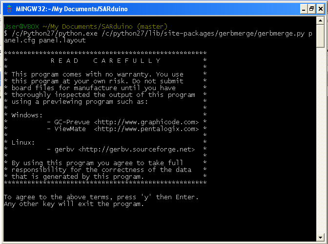
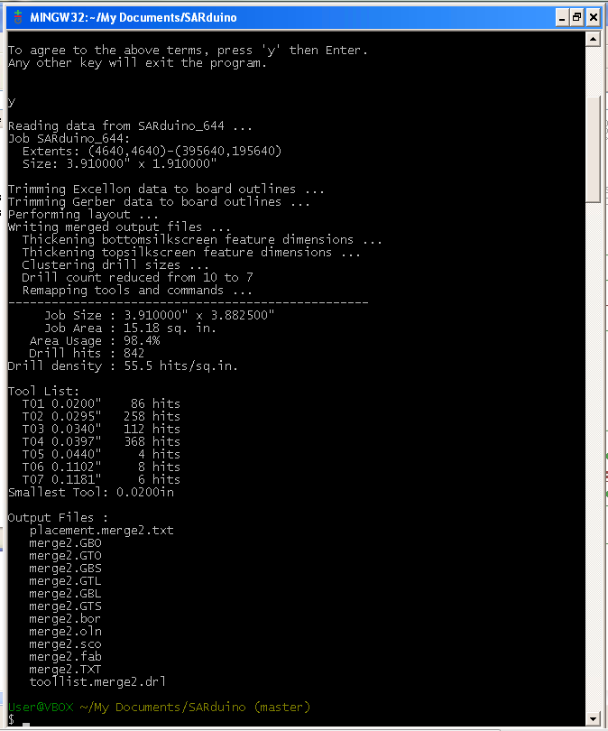
To generate the panel, invoke gerbmerge as follows, with the panel configuration file first, and the layout file second, for example:
path/to/python path/to/gerbmerge.py panel.cfg panel.layout
You will first be presented with a warning about the lack of warranty, as in the first image below. Enter 'Y' to continue.
You should then shortly see output like in the second image below.
Have a look at the output in your favorite gerber viewer, to make sure the results are as you expected.
Repeat from step 1 until you are happy with the results.
Order PCBs
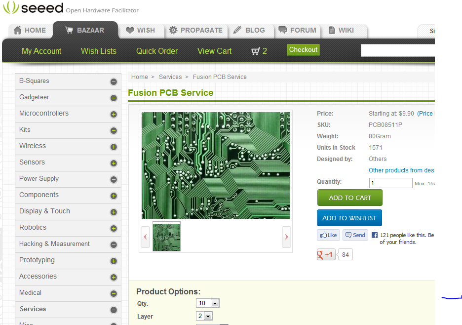
Follow all of Seeed's instructions for faster processing. As mentioned earlier, you may want to place your order before you go through the panelizing process, so that you can add your order number to the silk layer as required.
Separate PCBs From Panel
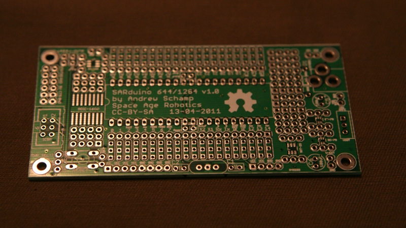
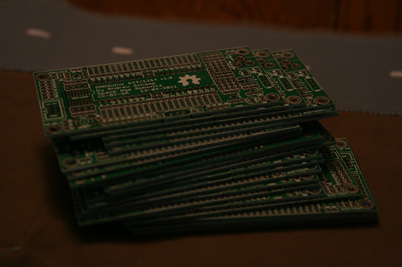
Once you have your boards, you need to cut them apart. I found that a bandsaw worked well, there was plenty of room for the blade between the boards, and I had a good guide that made a perfect edge. After cutting them, I cleaned up the cut edges by running them by hand over a (powered off!) belt sander.
I didn't catch any photos of using the band saw, but this hackaday post has some good ones.
You can see the cut and finished boards in the images below.
I didn't catch any photos of using the band saw, but this hackaday post has some good ones.
You can see the cut and finished boards in the images below.