PCB Designing and Isolation Milling Using Only Free Software
by ähöüokul in Circuits > Electronics
185609 Views, 1089 Favorites, 0 Comments
PCB Designing and Isolation Milling Using Only Free Software
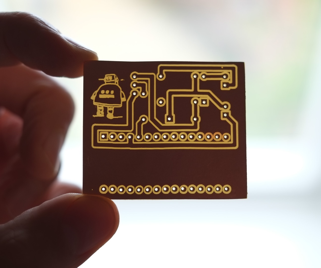
In this Instructable I will show you how to design and fabricate your own PCBs, exclusively using free software that runs on Windows as well as on a Mac.
Things you need:
- computer with internet connection
- cnc mill/router, the more accurate the better
- 45°/20° V-Bit
- 0.8mm drill bit
- 3mm endmill
- copper clad board
- double-sided adhesive tape
Get the Software
Designing in Fritzing
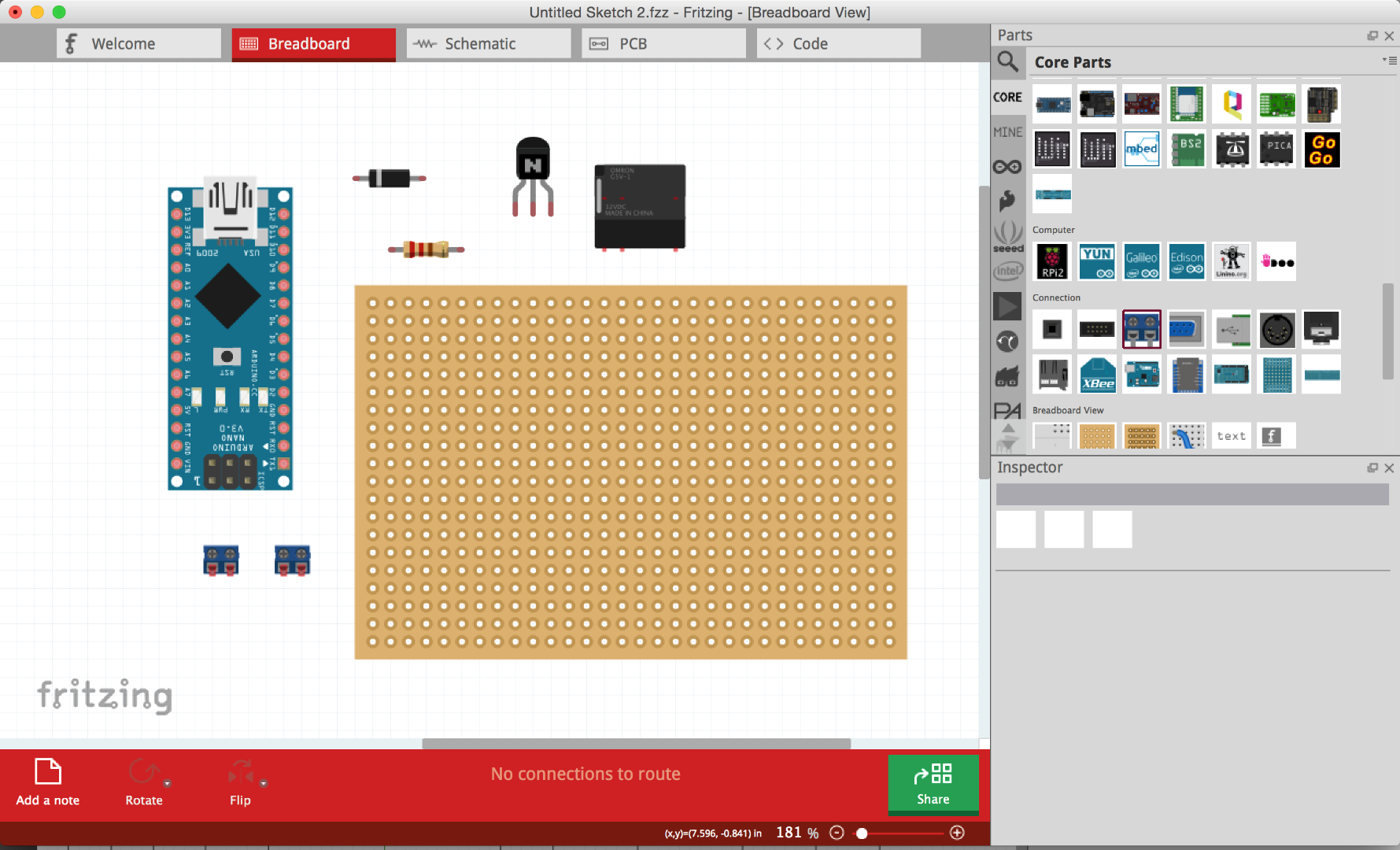
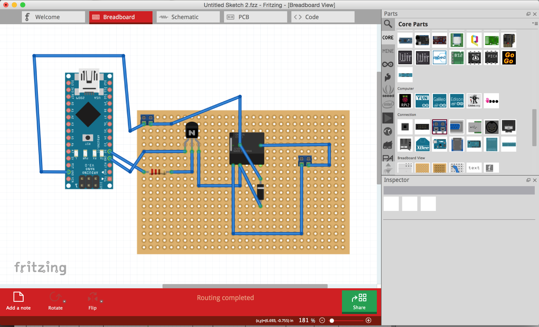
Start Fritzing and start a new sketch.
Go to breadboard view by clicking on the breadboard tab on the top of the window.
On the right side is your part-library, select the components you want in your circuit and drag&drop them into the breadboard window. Make sure the parts have the desired specs such as pinout, value and size. You can change these variables of the selected component in the Inspector to the lower right of your screen.
In this example I'm making a circuit that uses an Arduino Nano for switching a 12V relay. For this i need a transistor with a resistor to the base as well as a catch diode in parallel to the relay coil and two screw terminals.
The connections/wires between the components are made by clicking and dragging on a leg/pin of the component. Bendpoints in the wires can be made by clicking and dragging inside a wire.
Make all the connections you need and would do on a real breadboard for the circuit to work.
Schematic View
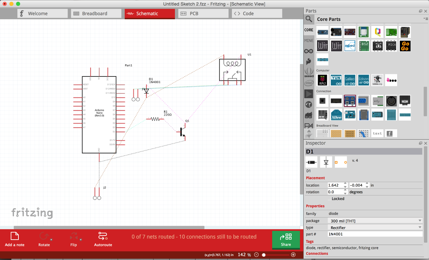
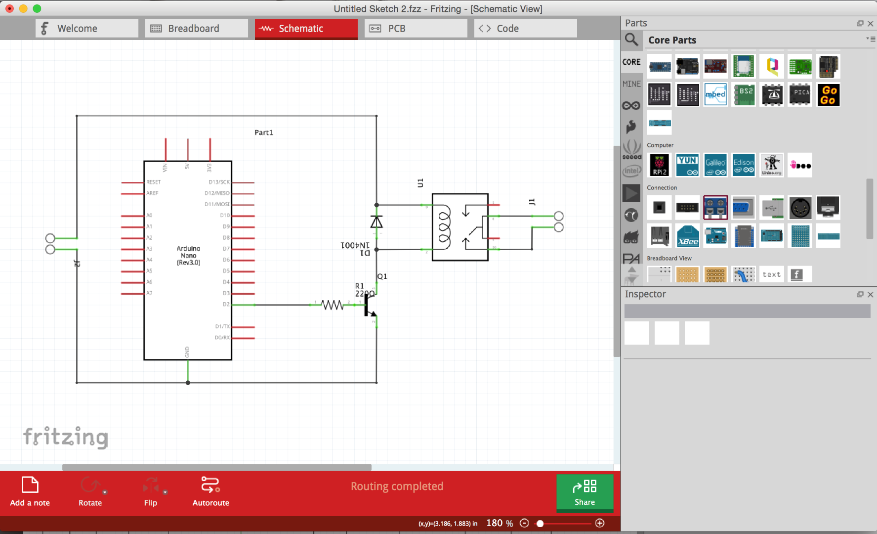
Now navigate to the Schematic View.
You will see a wiring diagram with all your components and their connections. Tidy things up by dragging the components in a reasonable order and clicking and dragging the dashed connection lines so they're not intersecting themselves.
PCB View
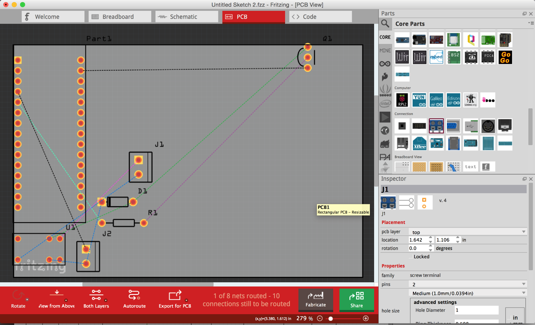
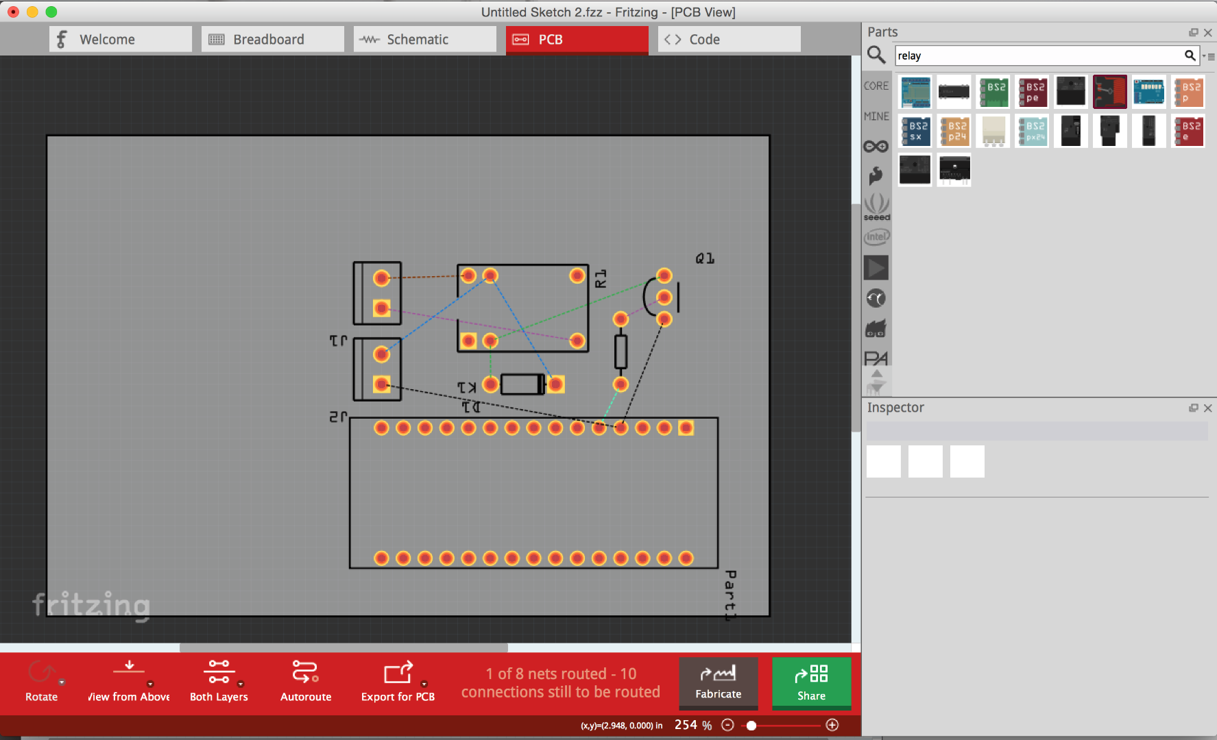
Go to PCB View.
Drag your components in a reasonable order. A good rule of thumb is to place the components with the most pins to the center and the other components around. Try to get a compact distribution.
The parts lock automatically to the grid you see in the background. For changing the grid size go to View -> Set grid size.
Autoroute
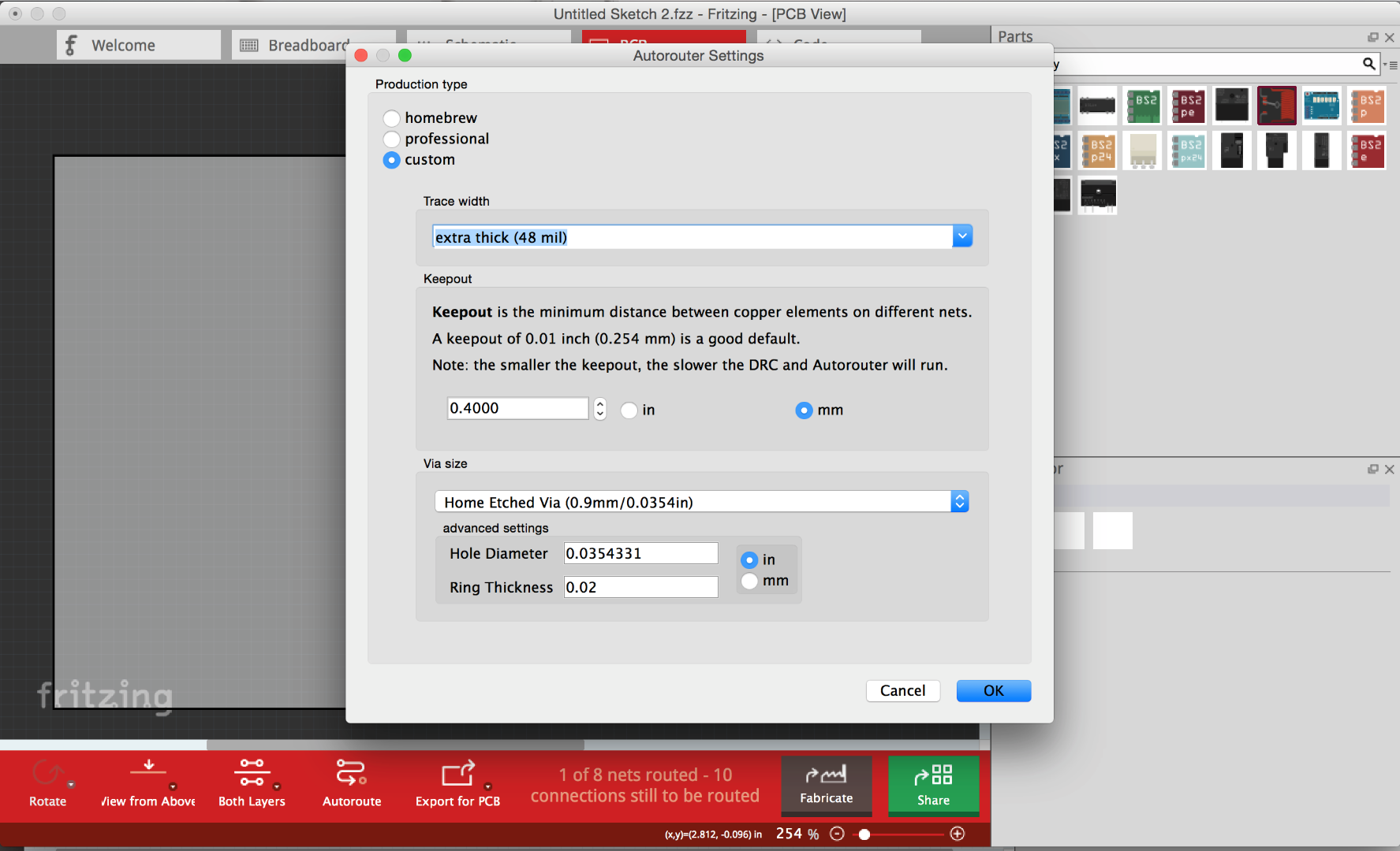
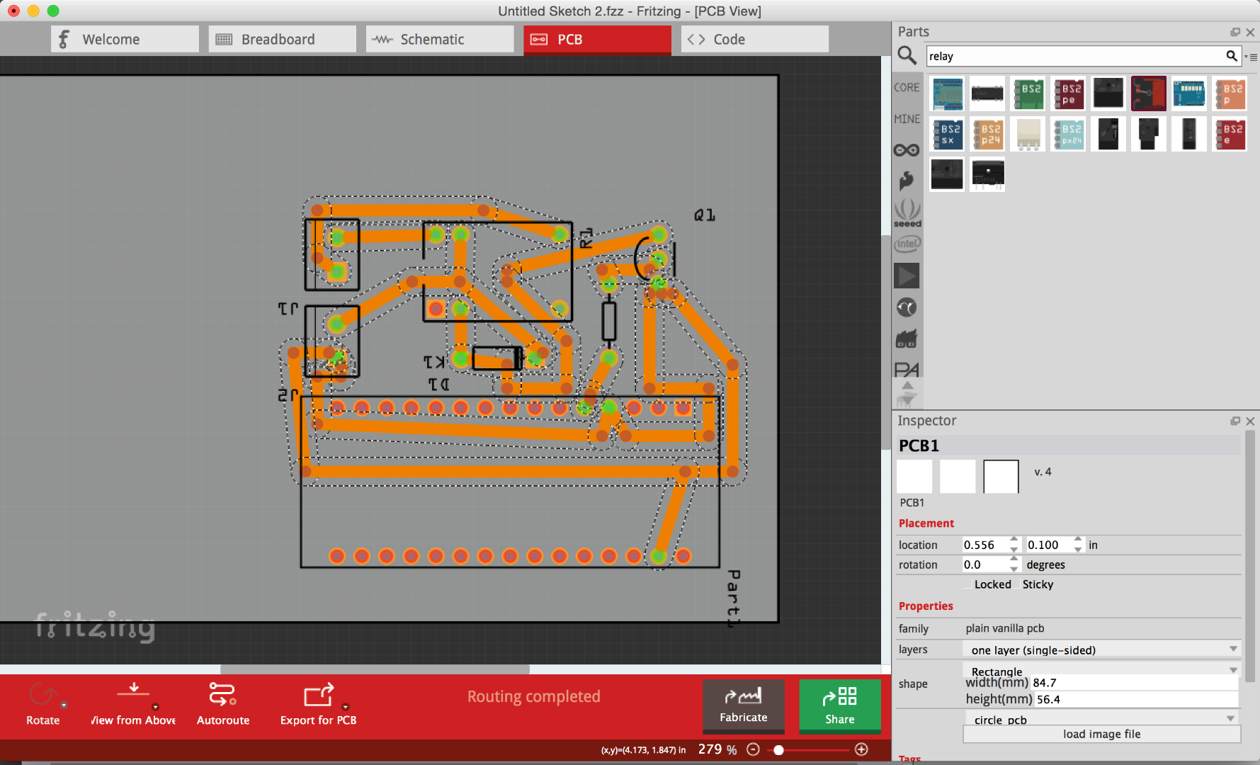
Click on Routing -> Autorouter/DRC settings and select custom production type. Now you can set the trace width to the desired thickness depending on your machine/endmill/circuit. I used 48mil. Click "OK".
Select the grey rectangle (the PCB Board) and in the Inspector change the layers-dropdown to "one layer (single sided)".
Now hit the Autoroute-button in the bottom of the window and let the computer do the routing work!
Some More Routing
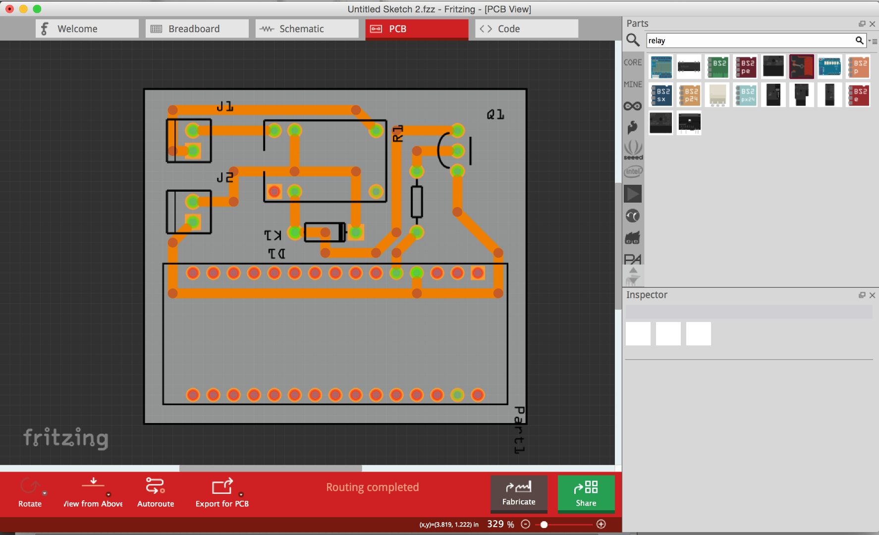
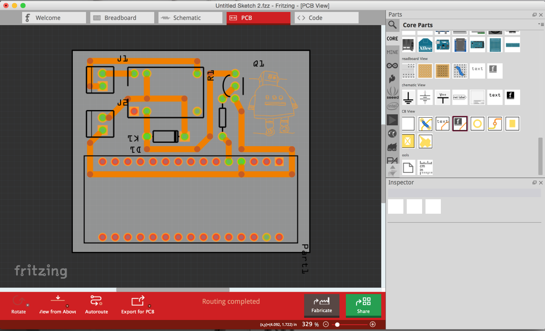
When the Autorouting is complete, tidy up the traces by clicking and dragging their bendpoints. Right click on the bendpoint and select remove bendpoint for removing it.
Sometimes there are connections the Autorouter cannot route. You have to route them by hand by clicking and dragging the dashed connection lines. Use Jumpers from the parts library for jumping over traces you otherwise would intersect.
You can also add text/logos that will show up in the copper mask by dragging "Silkscreen Image" or "Silkscreen Text" from the library to your board. Select your logo and in the Inspector under Placement - pcb layer dropdown menu select "copper bottom". you can load your own .svg files too by clicking on "load image file" in the inspector.
Check Your Circuit
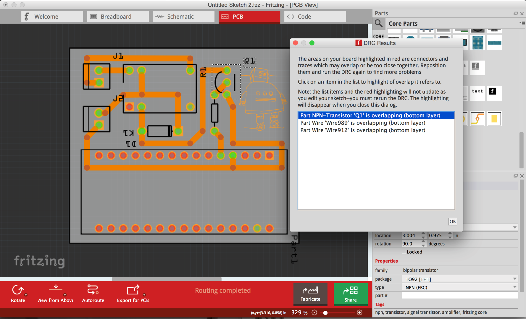
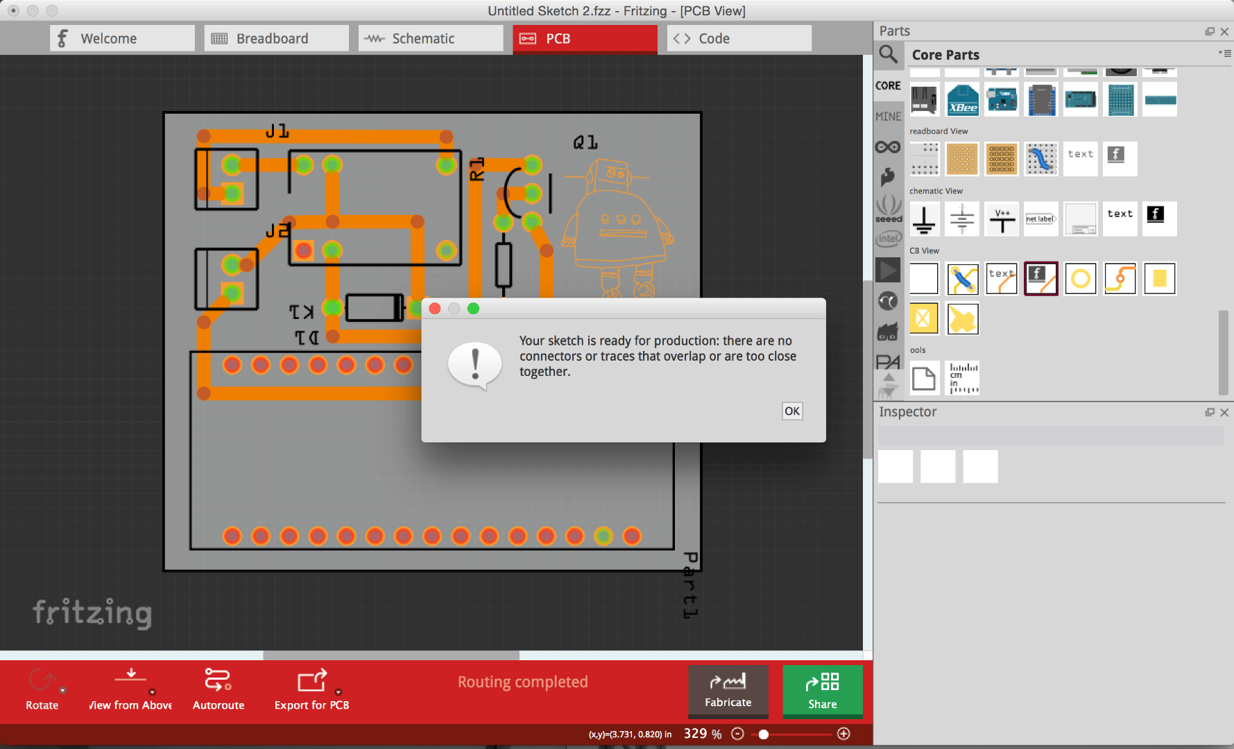
If you think you are ready with the routing click on Routing -> Design Rules Check for automatically checking your creation for missed connections / overlapping or intersecting traces.
Try to eliminate all errors and repeat the DRC until there are no more problems. Design is finished!
Export your PCB as .svg files by clicking on "Export for PCB" on the bottom. Click on the small arrow on the Export button and select "Etchable (SVG)".
You will get a bunch of svg's exported in your selected directory but we will only use two of them:
- *yourfilename*_etch_copper_bottom_mirror.svg
- *yourfilename*_etch_mask_bottom_mirror.svg
All other files can be deleted.
Inkscape
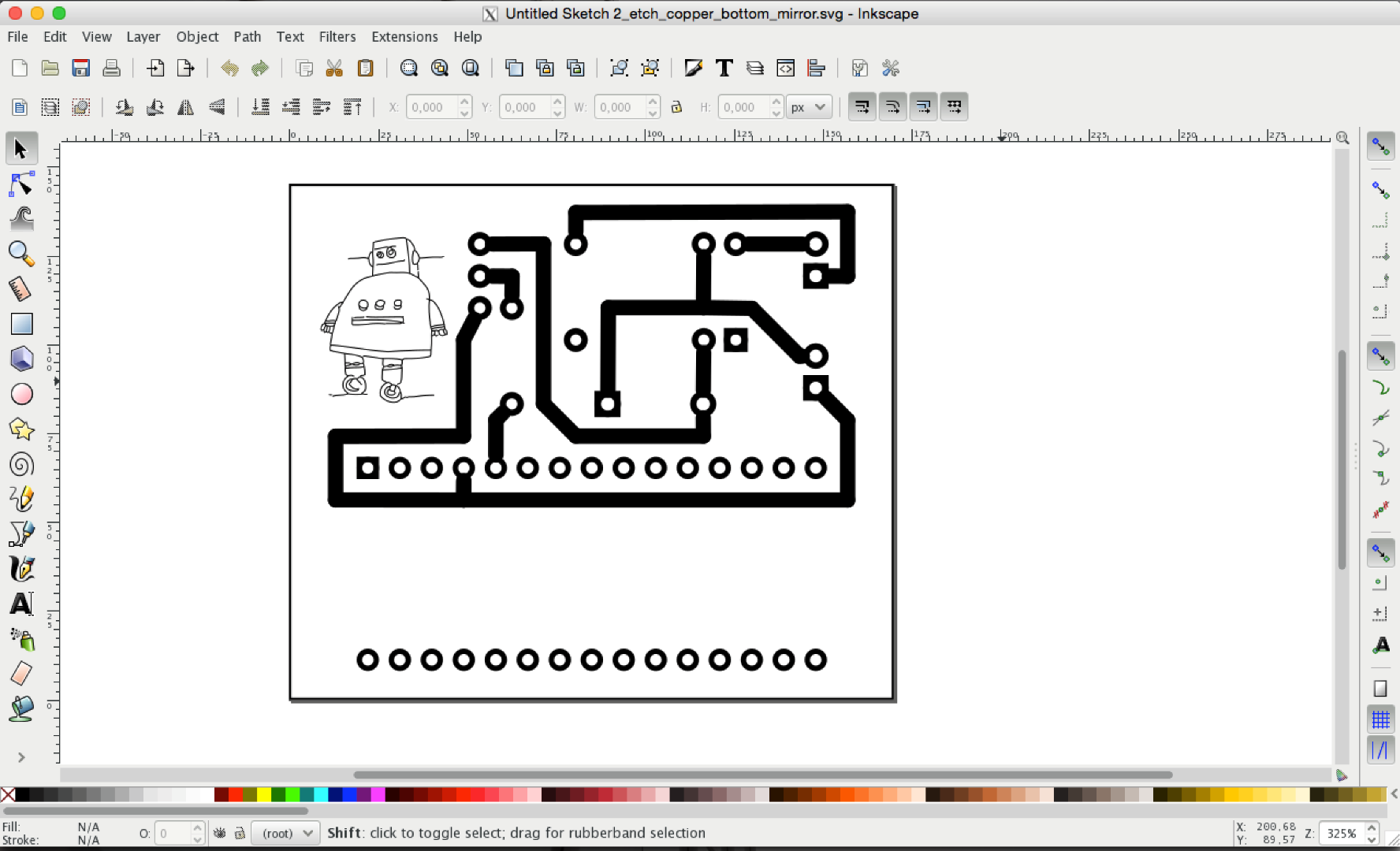
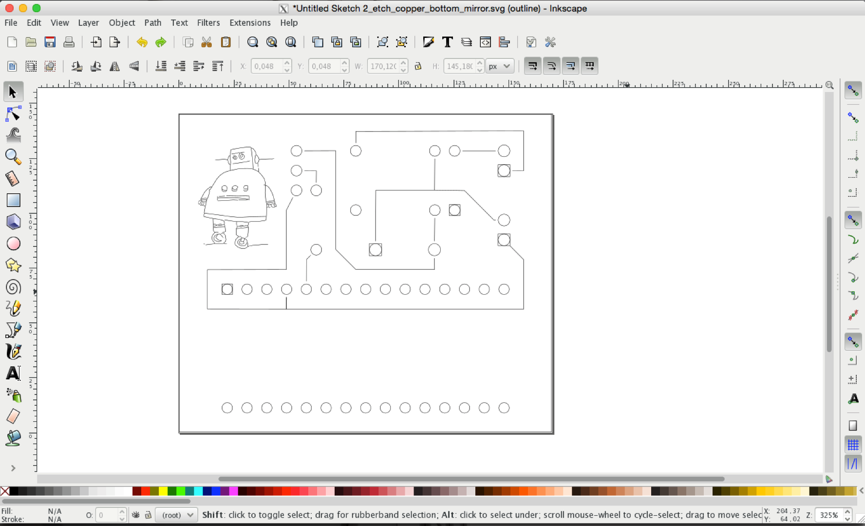
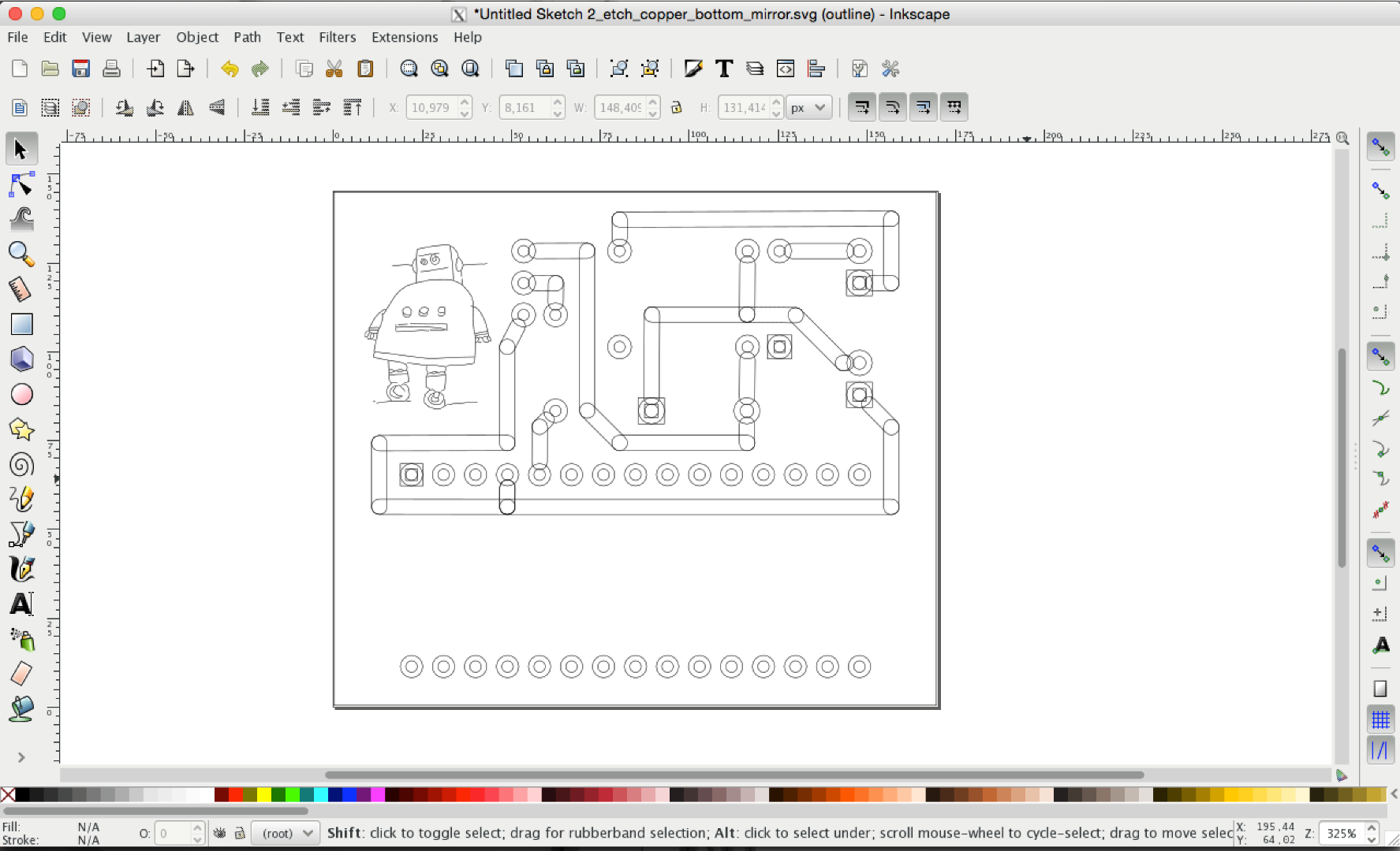
Open the *yourfilename*_etch_copper_bottom_mirror.svg in Inkscape, select everything and repeatedly press ctrl+shift+g until everything is ungrouped.
Select view -> display mode -> outline. You will now see only the vectors without fill or stroke.
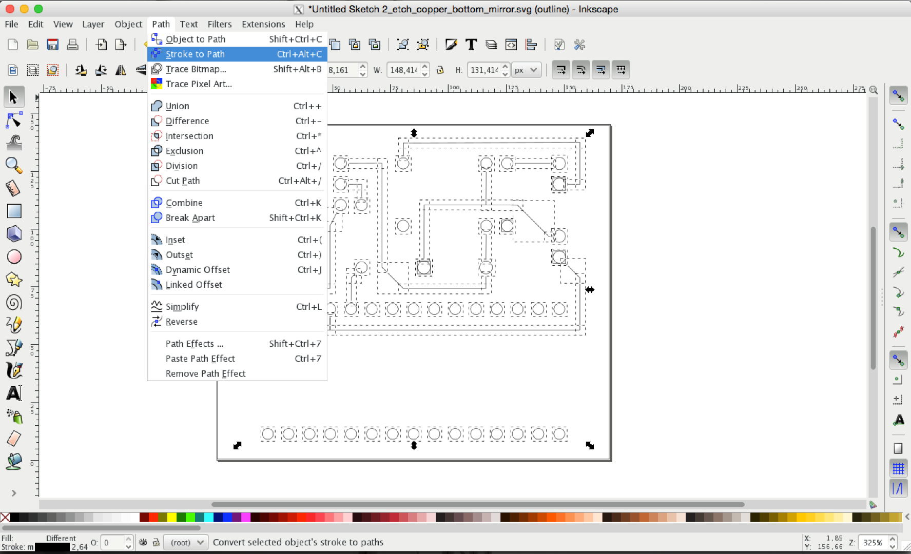
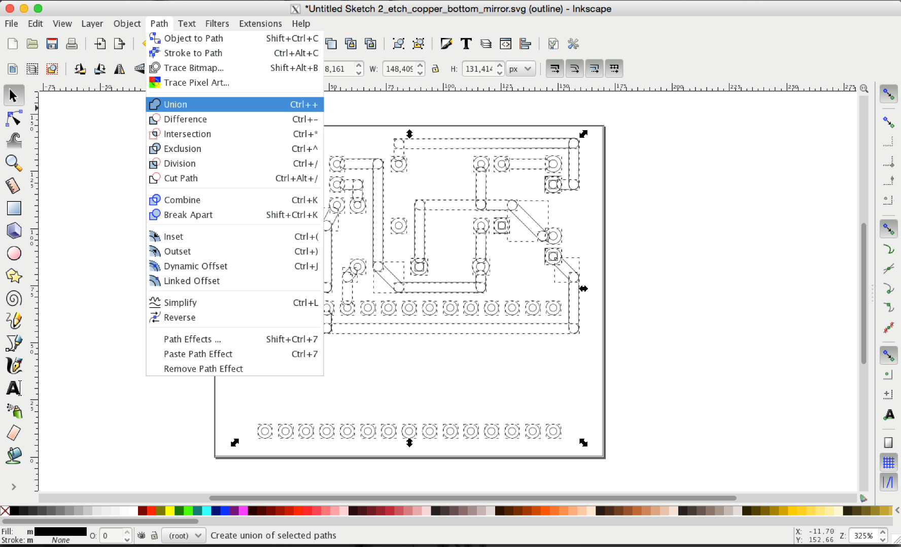
Select all traces and go to Path -> Stroke to Path.
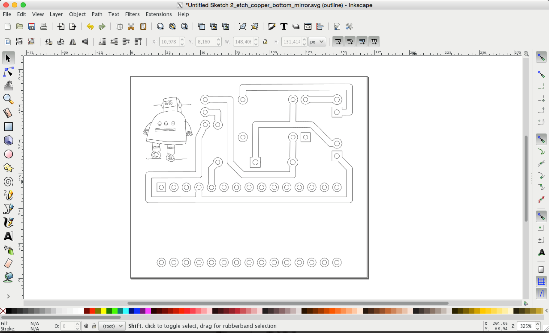
Select all traces and go to Path -> Union.
Save.
The file is now ready for CAM!
The other .svg we exported from fritzing doesn't need to be processed in Inkscape.
Makercam
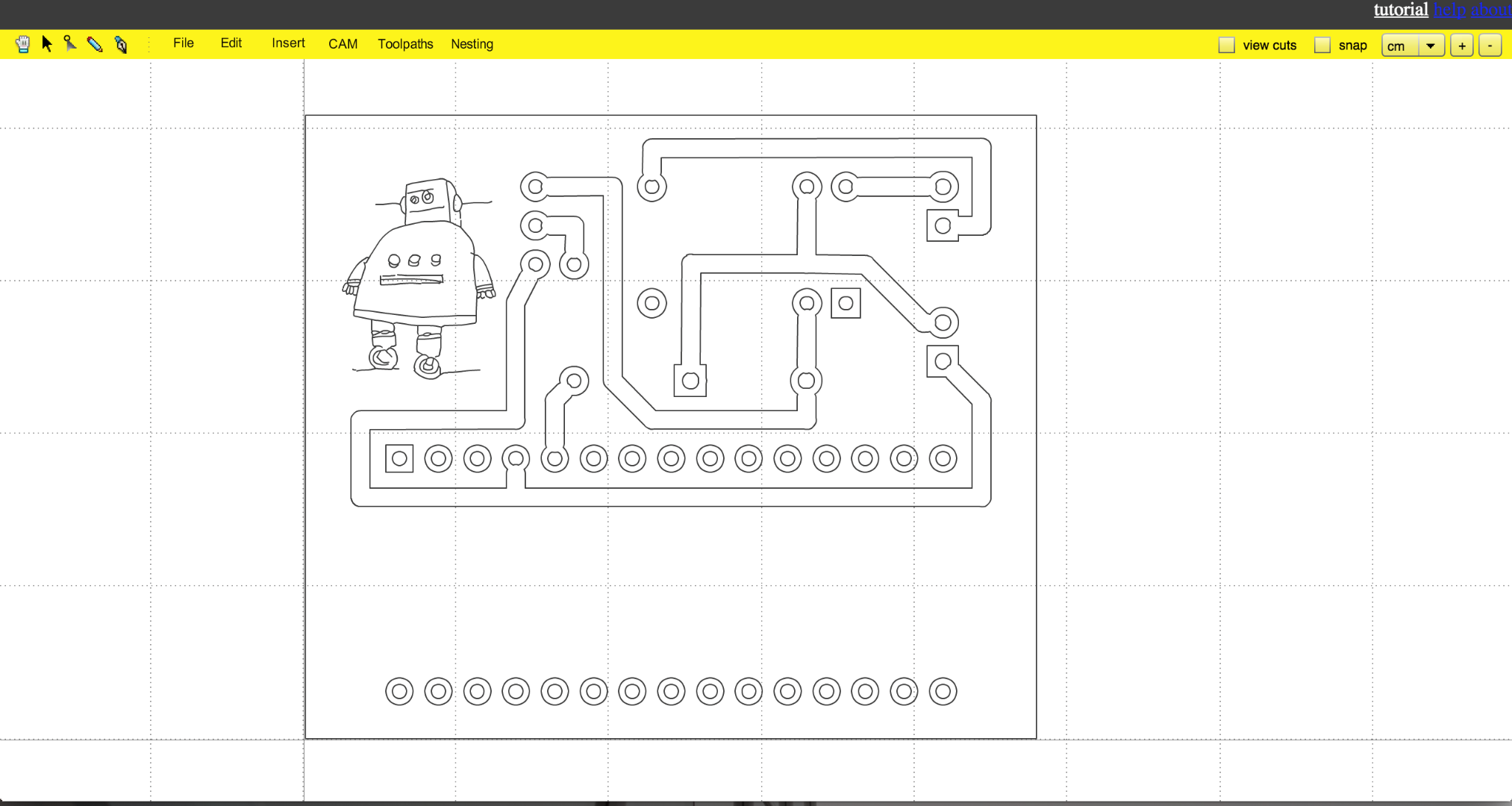
Open your browser and go to makercam.com.
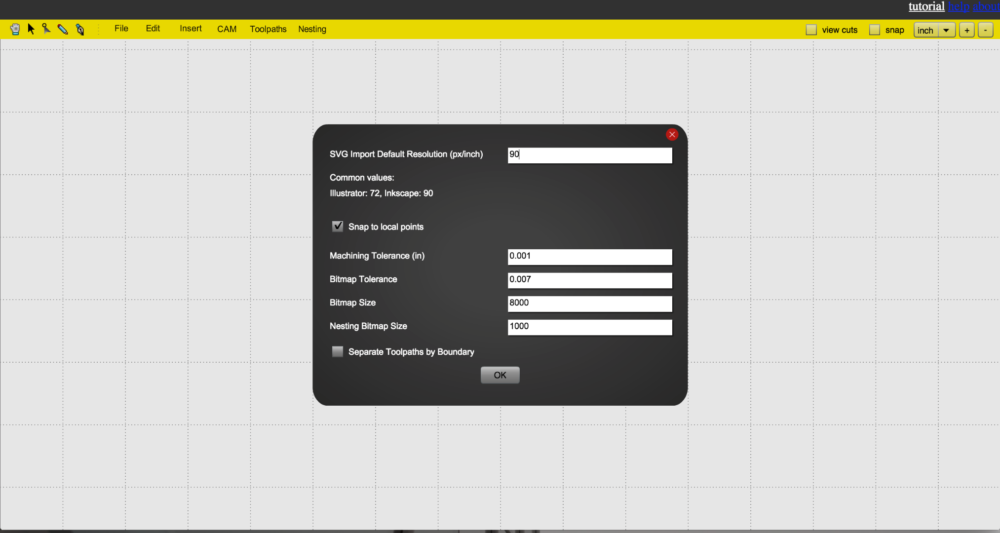
Go to Edit -> Edit preferences and change the SVG Import default resolution to 90 ppi.
Go to File -> Open SVG file, navigate to your directory and select the "*yourfilename*_etch_copper_bottom_mirror.svg" file.
Isolation Milling
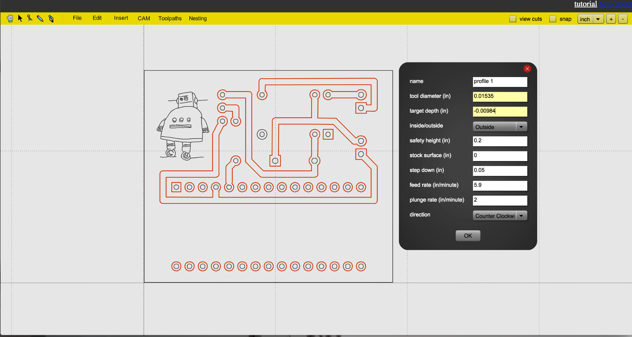
Select all your traces (but not the inner circles of the pins) and go to CAM -> profile operation.
If your CNC is GRBL based you may want to do all CAM in makercam in imperial units (see here for further reference). So you have to convert all your millimeters to inches before typing them in.
If you're using a 45° V-Bit with 0.2mm tip for the isolation milling process and dive 0.25mm into the material, the effective tool diameter at the surface of your copper clad board is 0.39mm. This converts to 0,015354331 inches, Yayy!
As said, we want to go 0.25mm deep in the board, so we're typing -0.0098425197 inches as our target depth. The step-down value should be bigger than that so the cutter goes through in one single pass.
I found a feed rate of 150mm/min and a plunge rate of 50mm/min to be working well on my machine.
Click OK.
Logo
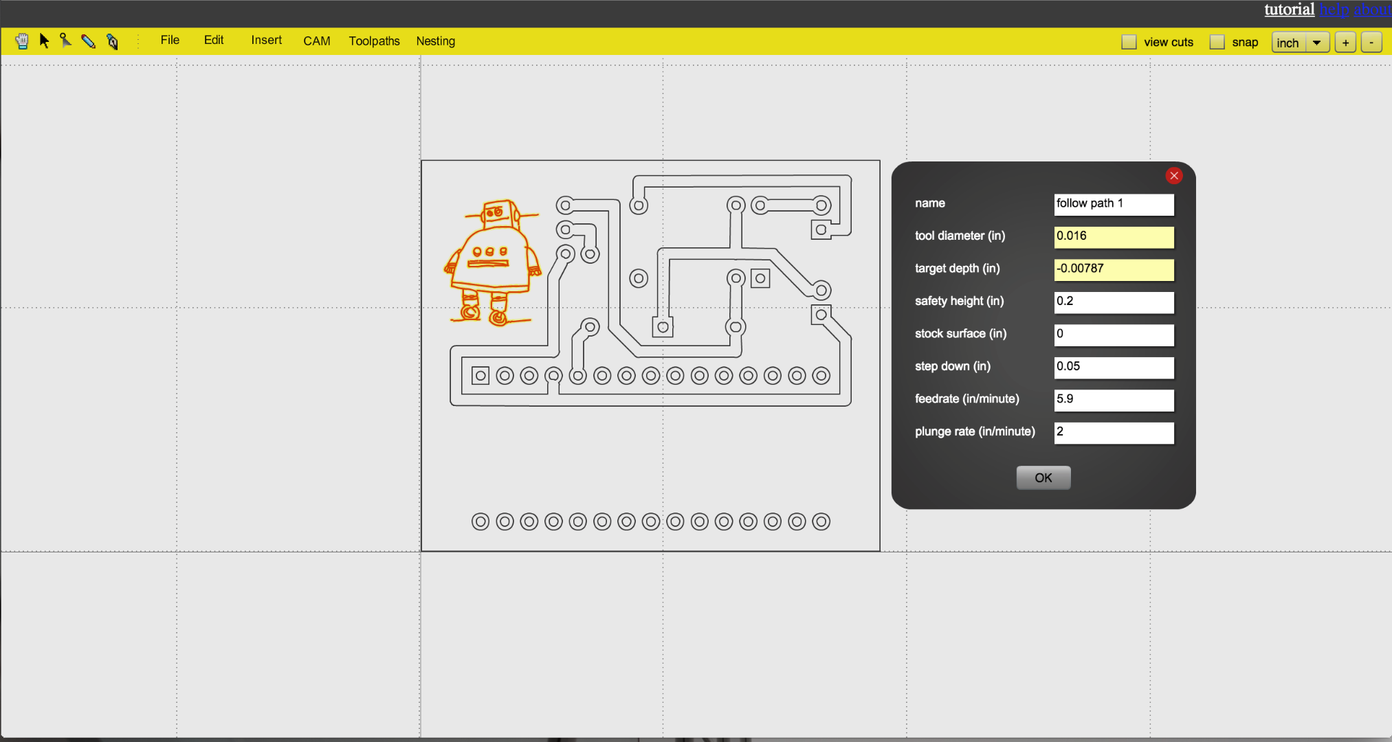
Select the logo/text and go to CAM -> follow path operation.
For more detail in the logo, I used a 20° 0.2mm V-Bit. Since with this operation the center of your cutter follows the paths (as opposed to the profile operation where the "edge" of the cutter follows the path), it's not critical what you type in as for tool diameter.
Target depth is this time -0.2mm (for more detail).
All other values are the same as for the isolation milling.
Click OK.
Contour Pass
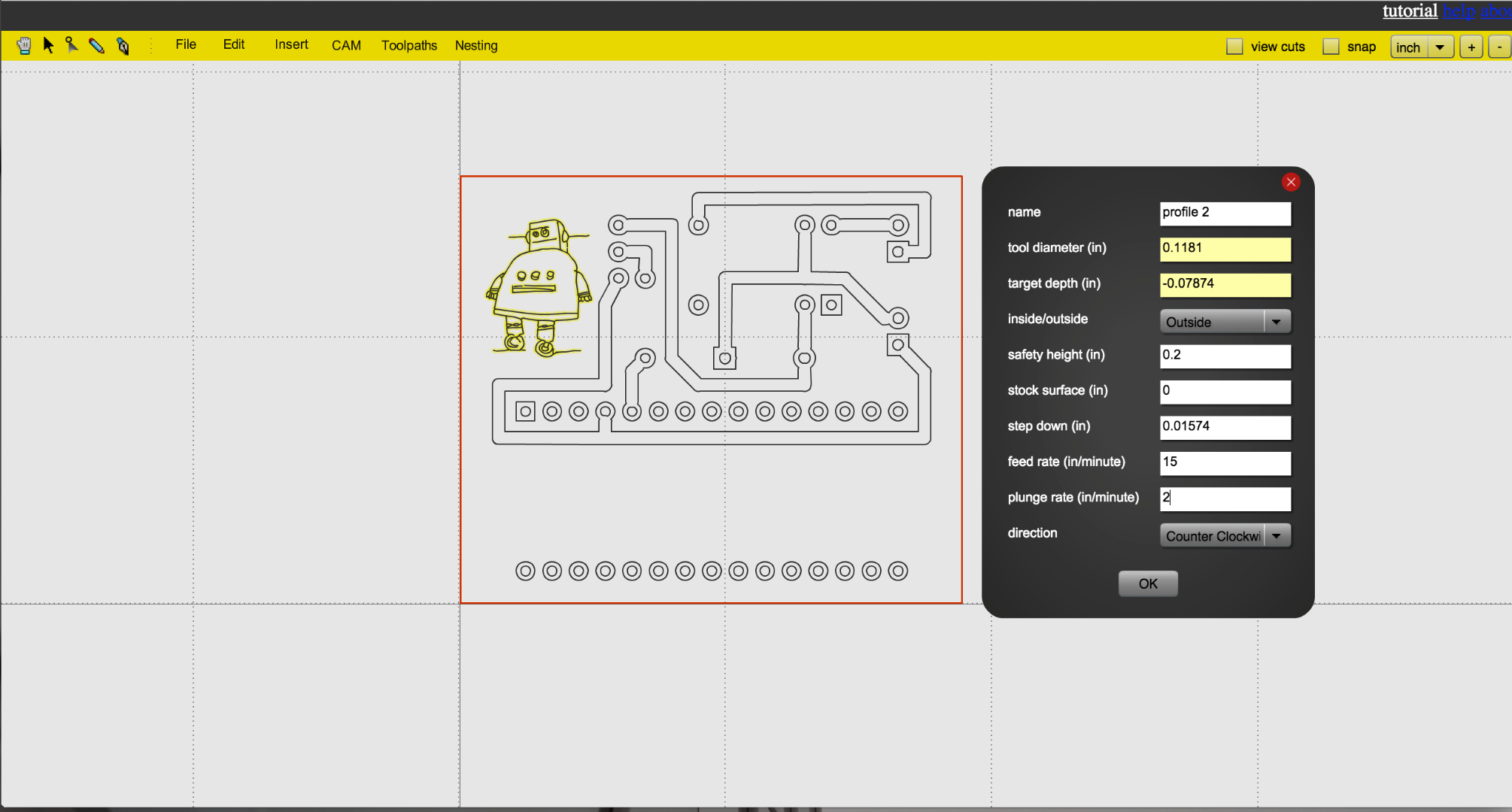
Now we want to cut our PCB out of the stock copper clad board.
Select the outer contour and type in the required values.
I used a 3mm 4-flute bit with a feed of around 400mm/min and a plunge of 50mm/min. Step down was 0.4mm.
Click OK.
Go to CAM -> calculate all.
Go to CAM -> export gcode.
Export every operation in a single file. Since every operation needs another tool, it's best to name the files after the tool.
Drilling
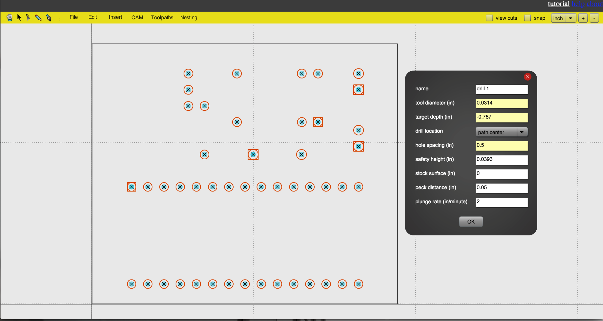
Reload the page so you're starting a "new project".
Open the "*yourfilename*_etch_mask_bottom_mirror.svg" file. Don't forget to change the SVG-scaling to 90ppi before doing so!
Select all holes.
Go to CAM -> drill operation.
I used a 0.8mm drill bit. My board was 1.5mm thick, so for a clean hole i used -2mm for the target depth. Peck distance should be bigger than this value for the drill to go through in a single pass. I used a plunge rate of about 50mm/min.
Click OK and all holes get automatically detected.
Go to CAM -> calculate all.
Export your gcode.
Preparing the Machine
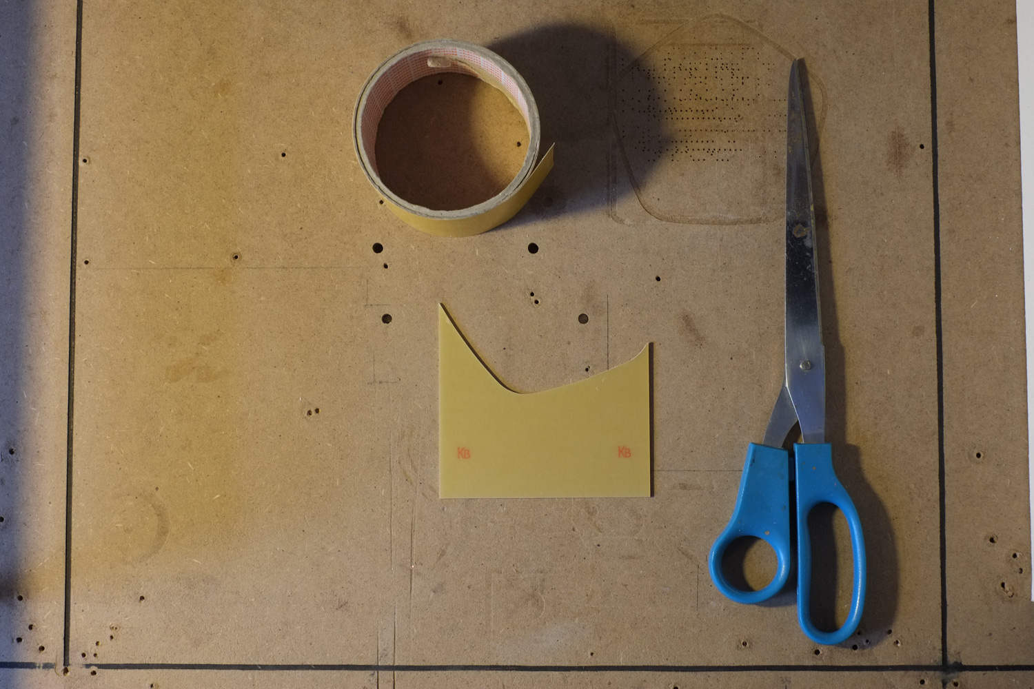
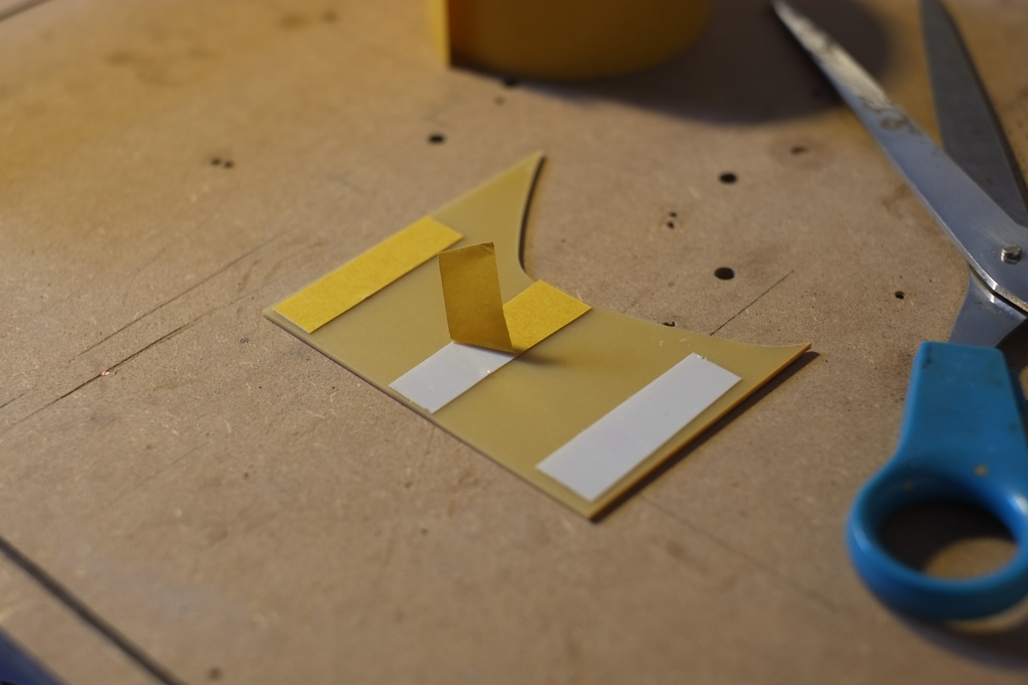
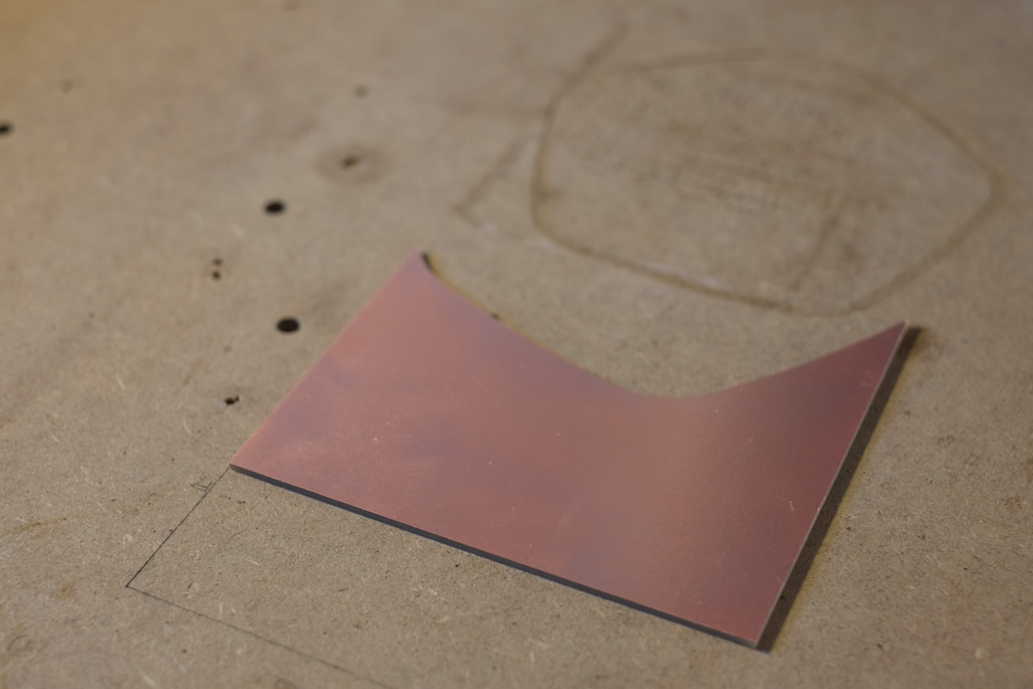
Use some strips of double-sided tape to glue down the copper clad board to the spoilboard of your machine.
Make sure that this part of the spoilboard is completely level, for example you can level it with milling a pocket (just needs to be 0.5mm deep) into it.
Or use an autoleveller. For the GRBL users this can be done by using chilipeppr.
Start Milling...
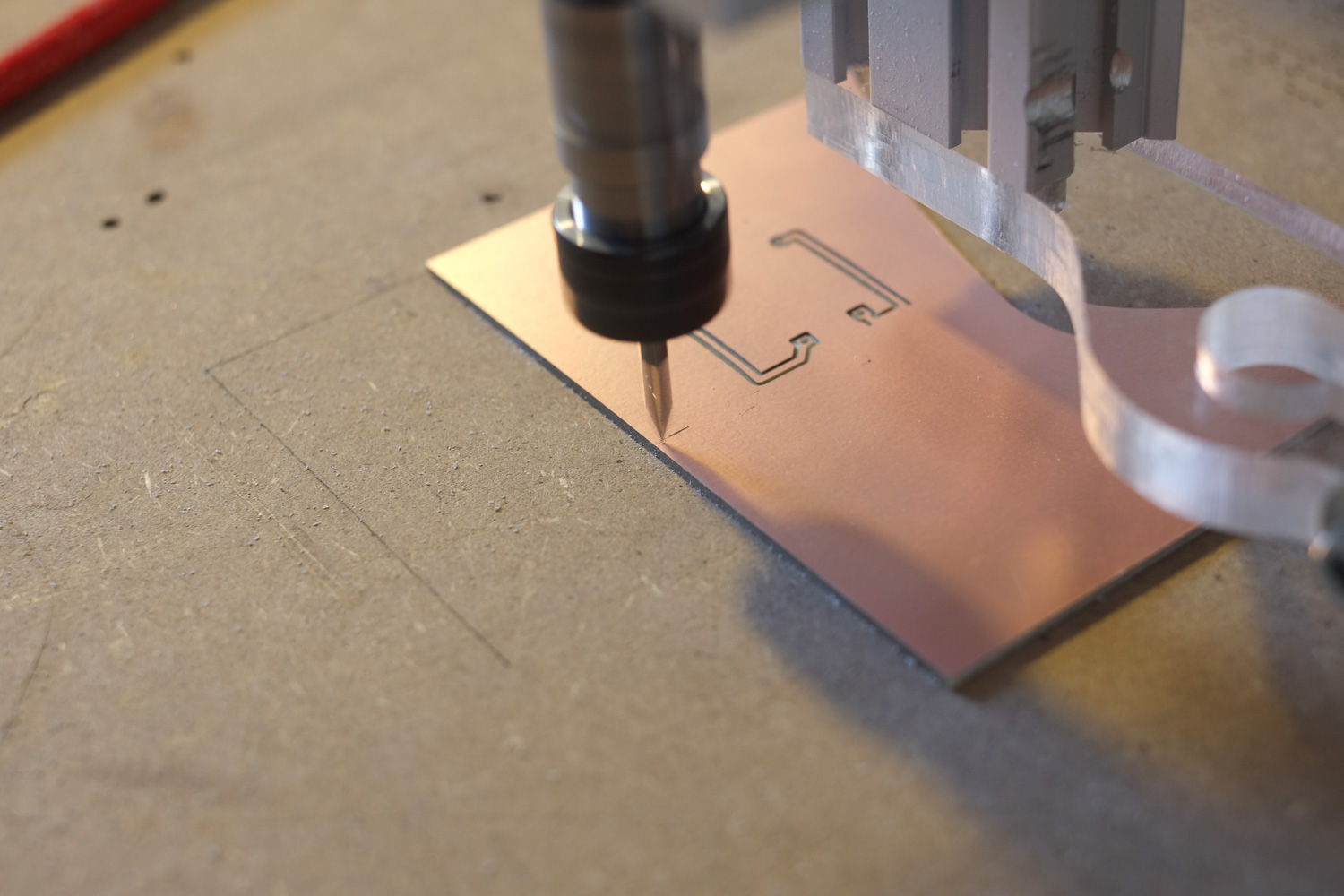
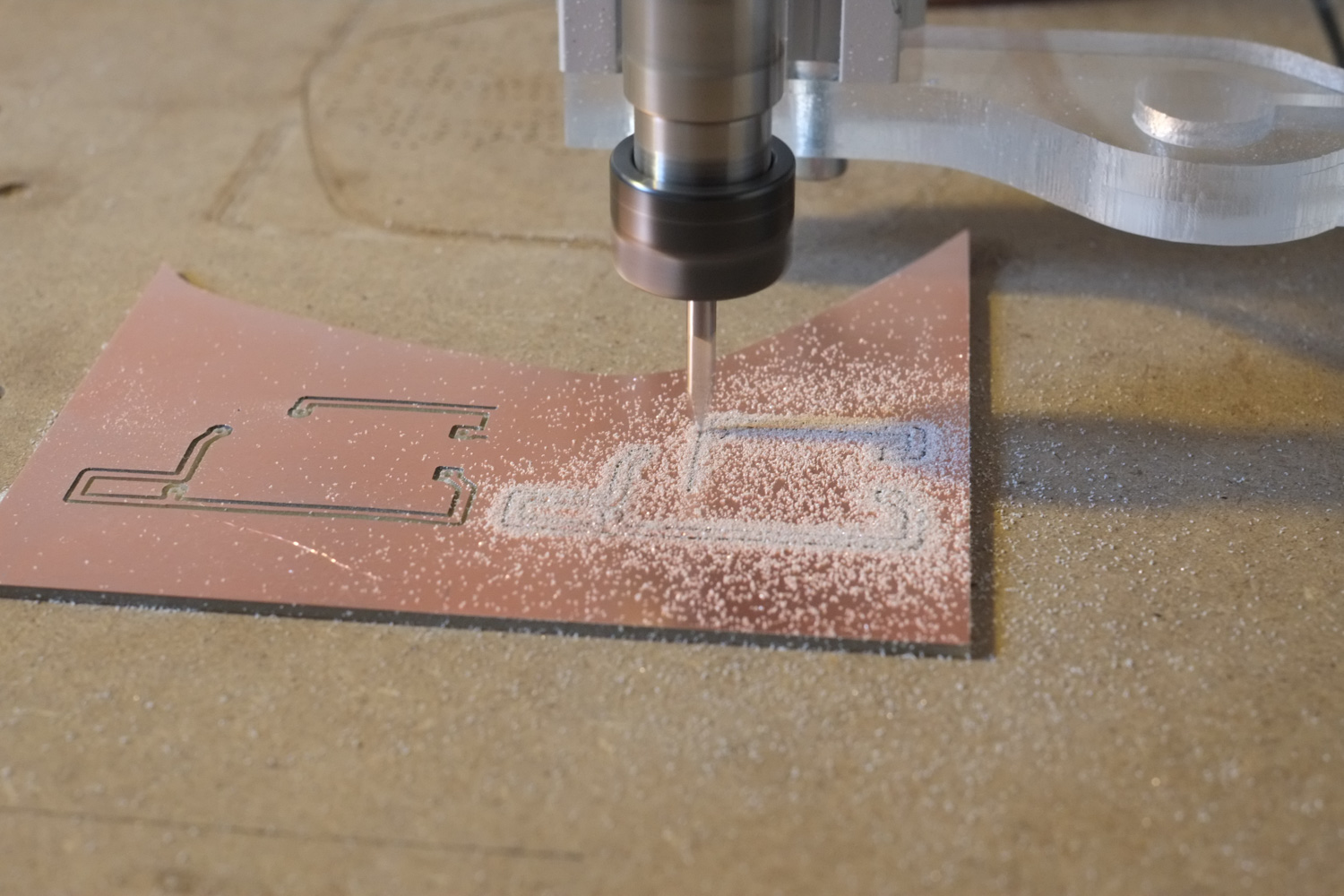
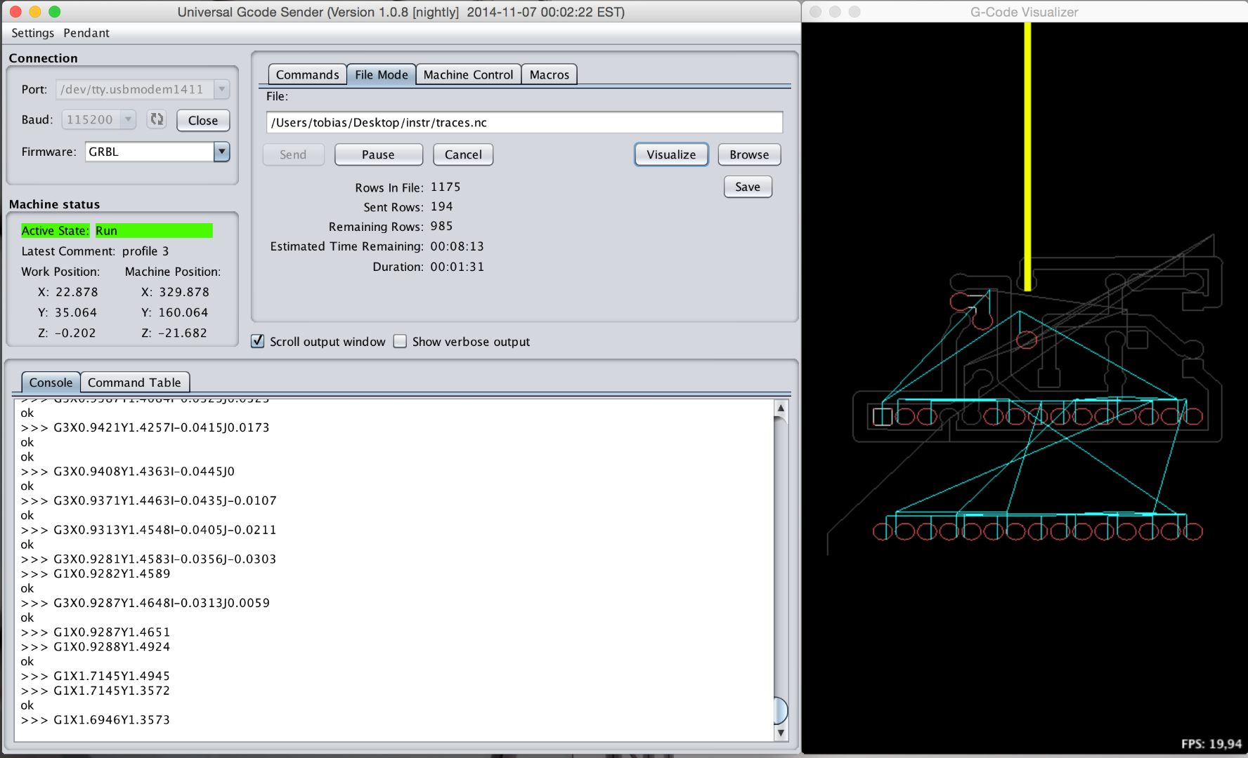
Load the 45° V-Bit
The zero location of the gcode files is on the lower left corner and on top of the stock surface.
So navigate your machine near to the lower left corner of the stock and lower the spindle so the tip of the bit barely touches the surface. Set this as your zero location and start the isolation milling.
...drilling...
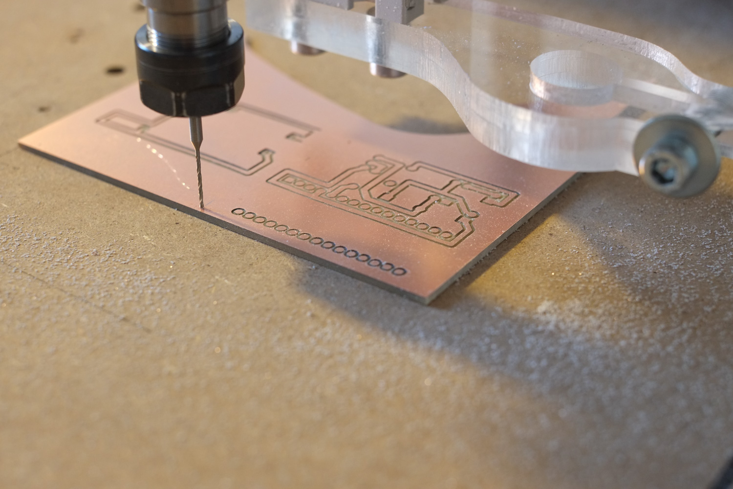
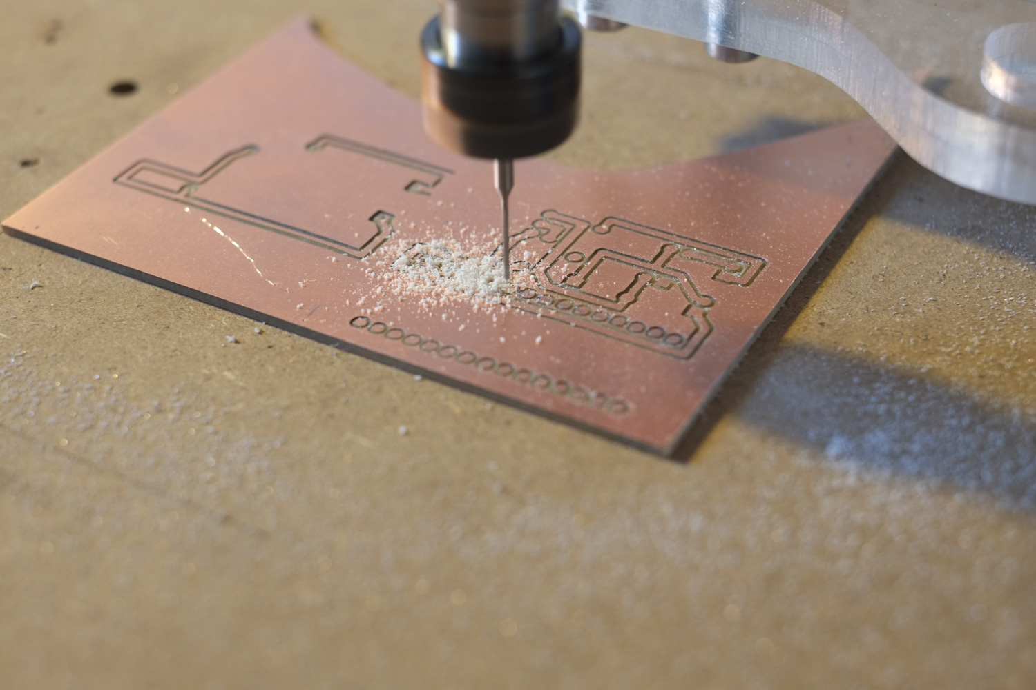
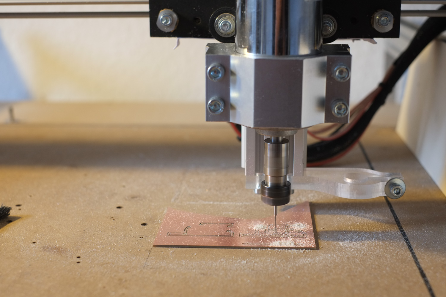
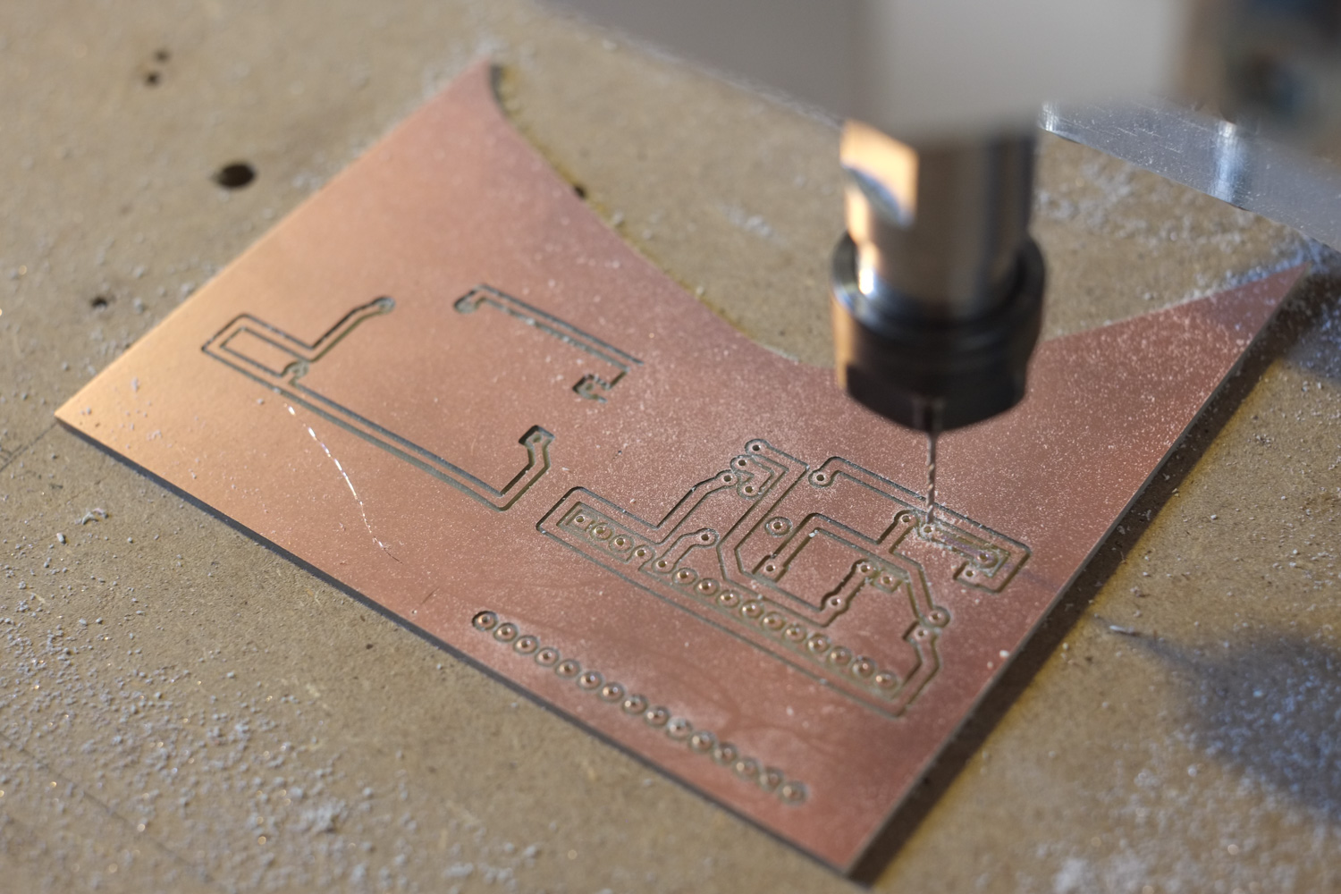
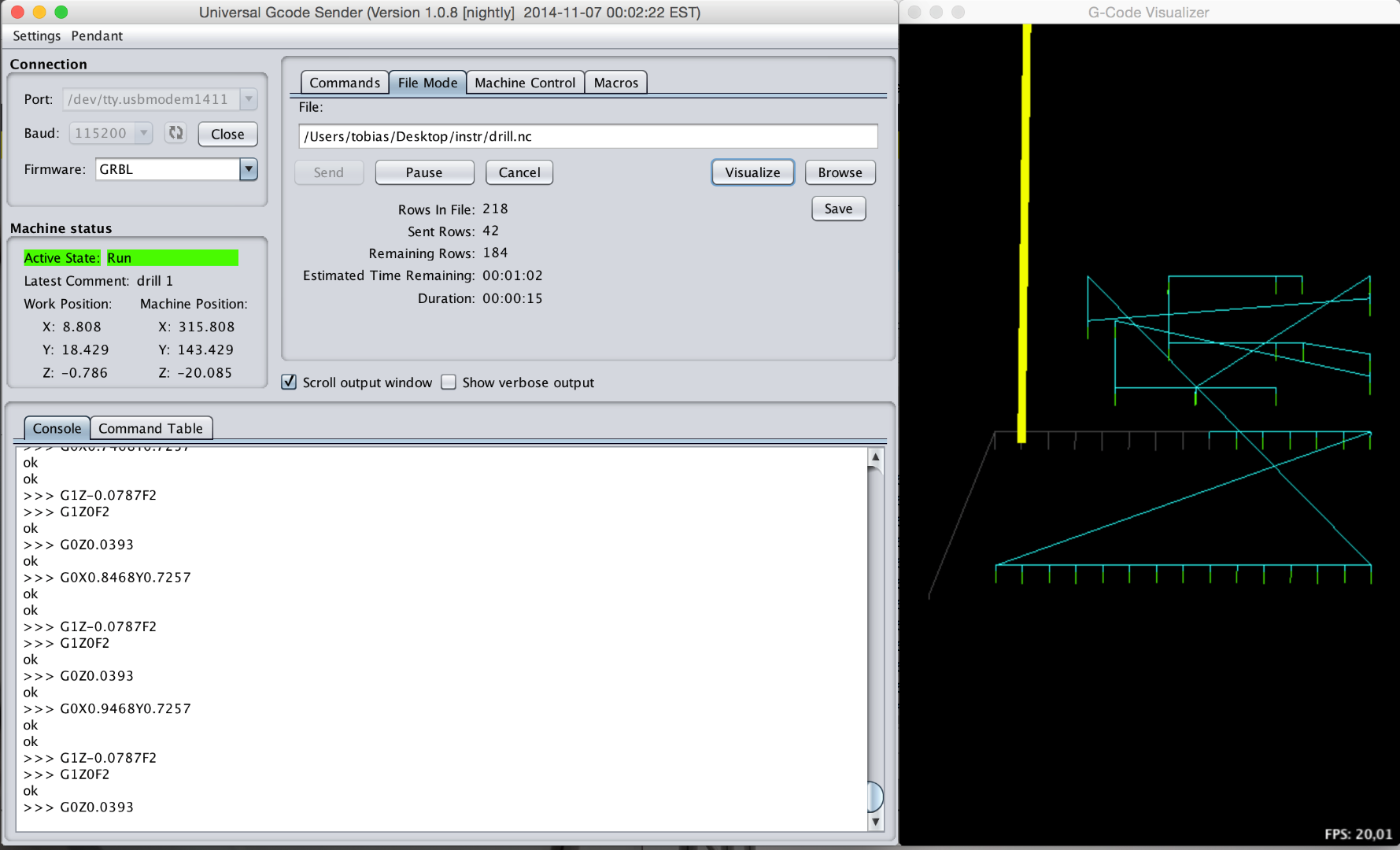
Change the tool to a 0.8mm drill bit and set your new Z zero when the tip is touching the surface. Start drilling the holes.
...engraving
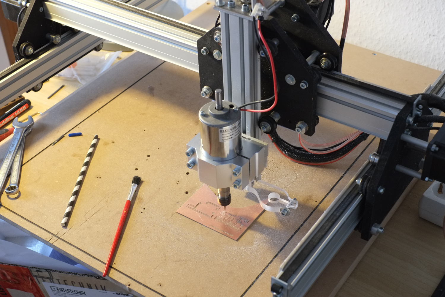
Change the tool to the 20° V-Bit and start the follow path operation for engraving the logo/text.
Cut Out
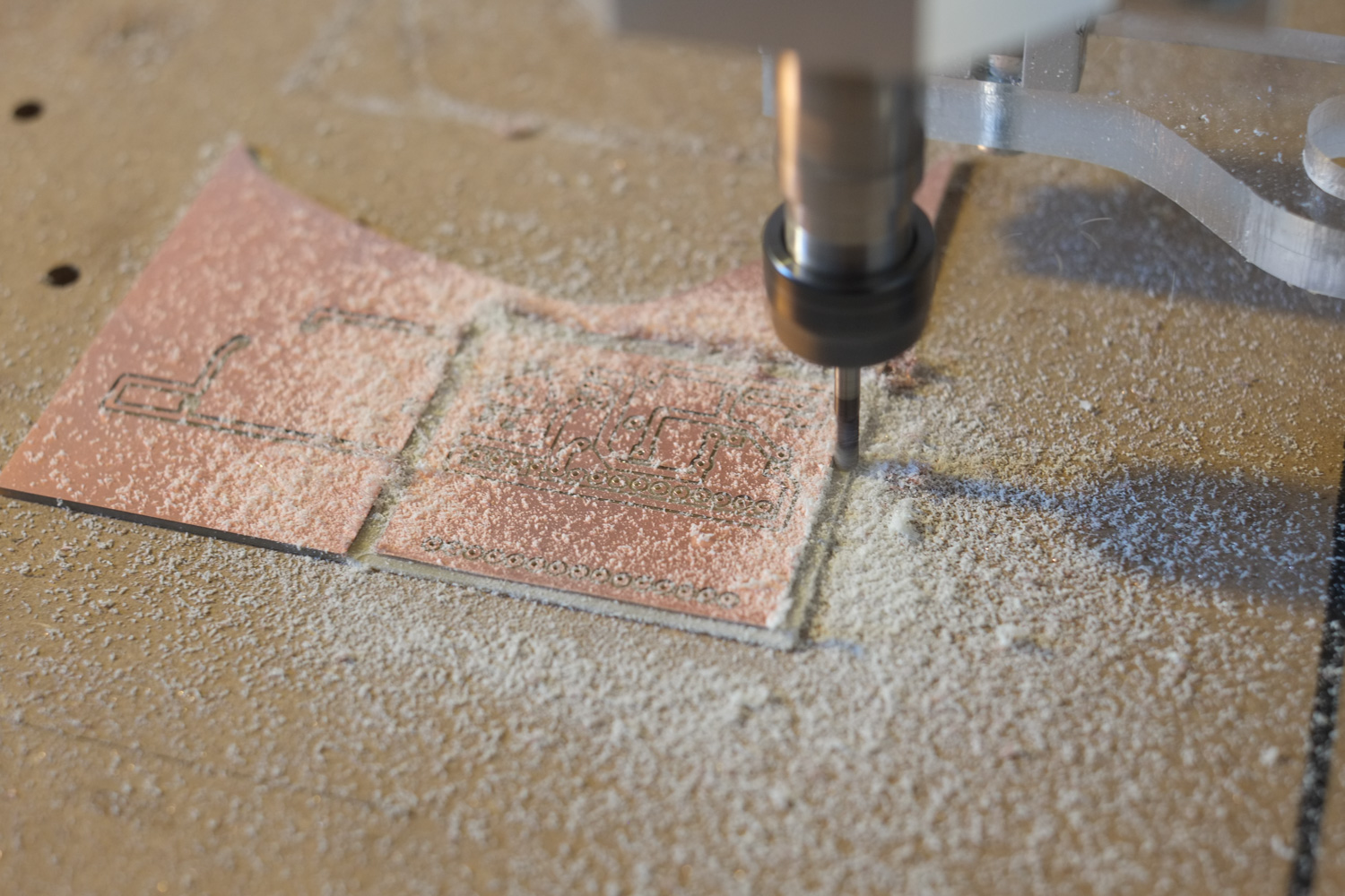
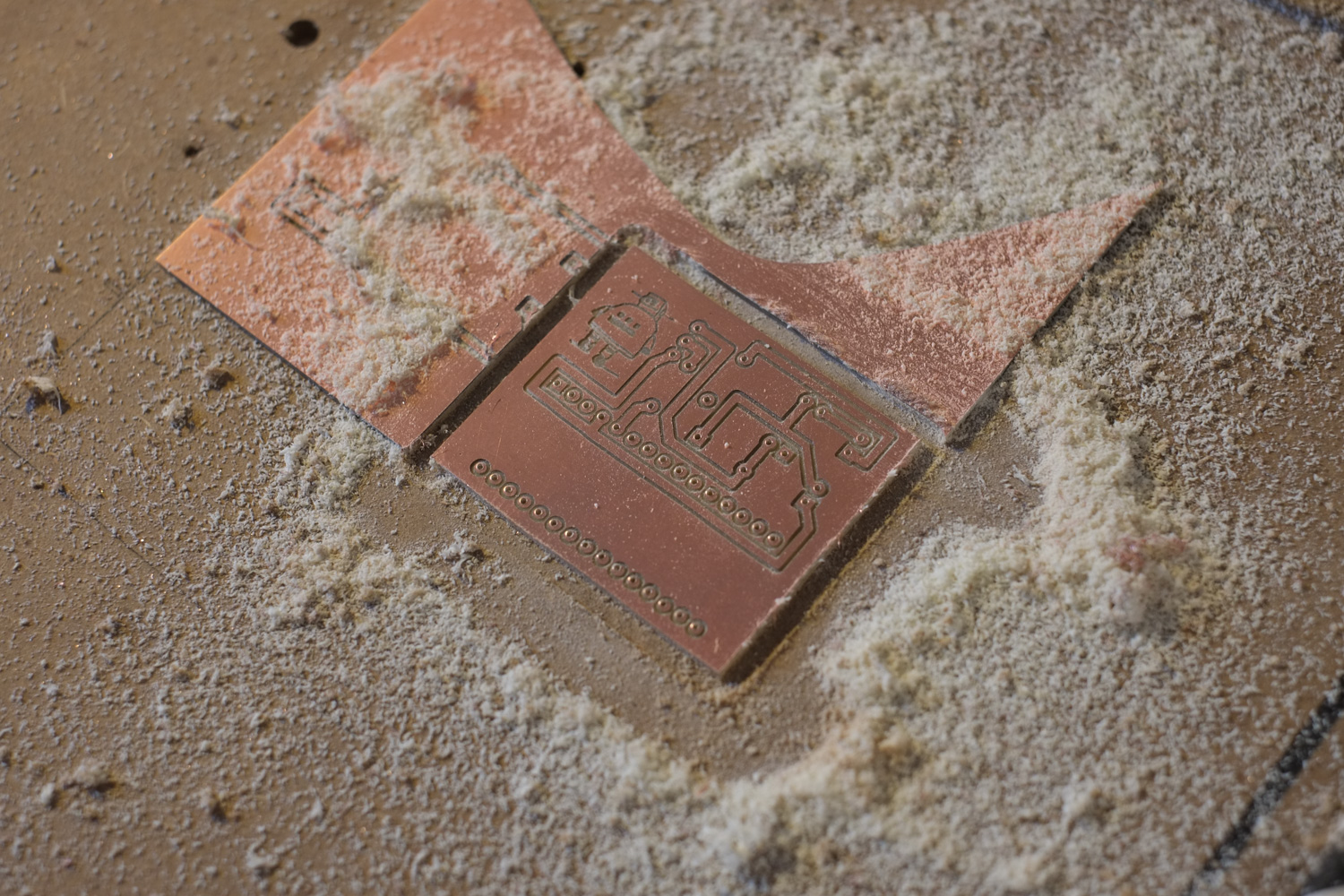
The last step is to cut the PCB out of the stock material.
Use the 3mm endmill and the second profile operation to do so.
Success!
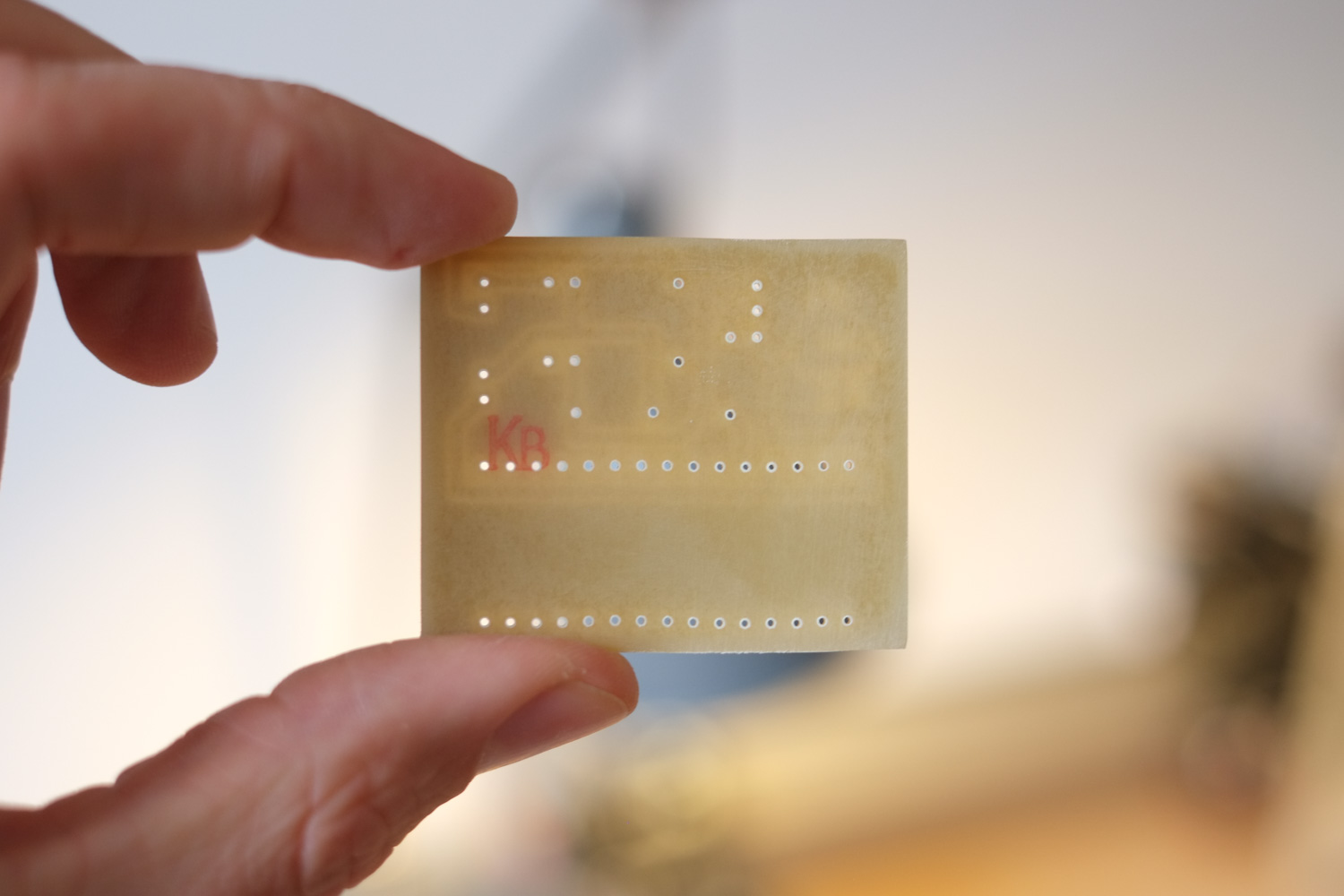
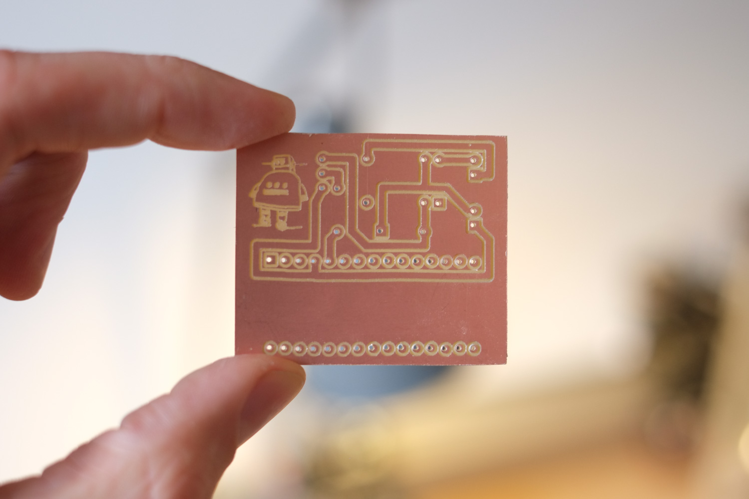
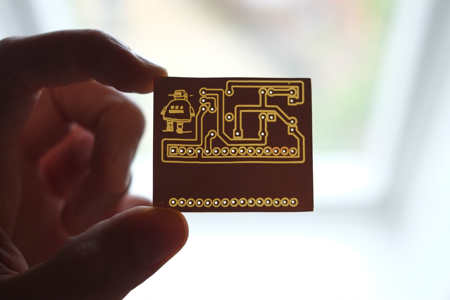
There you go with your new homemade PCB!
If you're fast (and your design is not too complex) you can make it from idea to product in under 1h.
I hope this Tutorial helps you in your projects and if you want you can vote for me on the top of this page or here. Thank you!