PCB Visiting Card
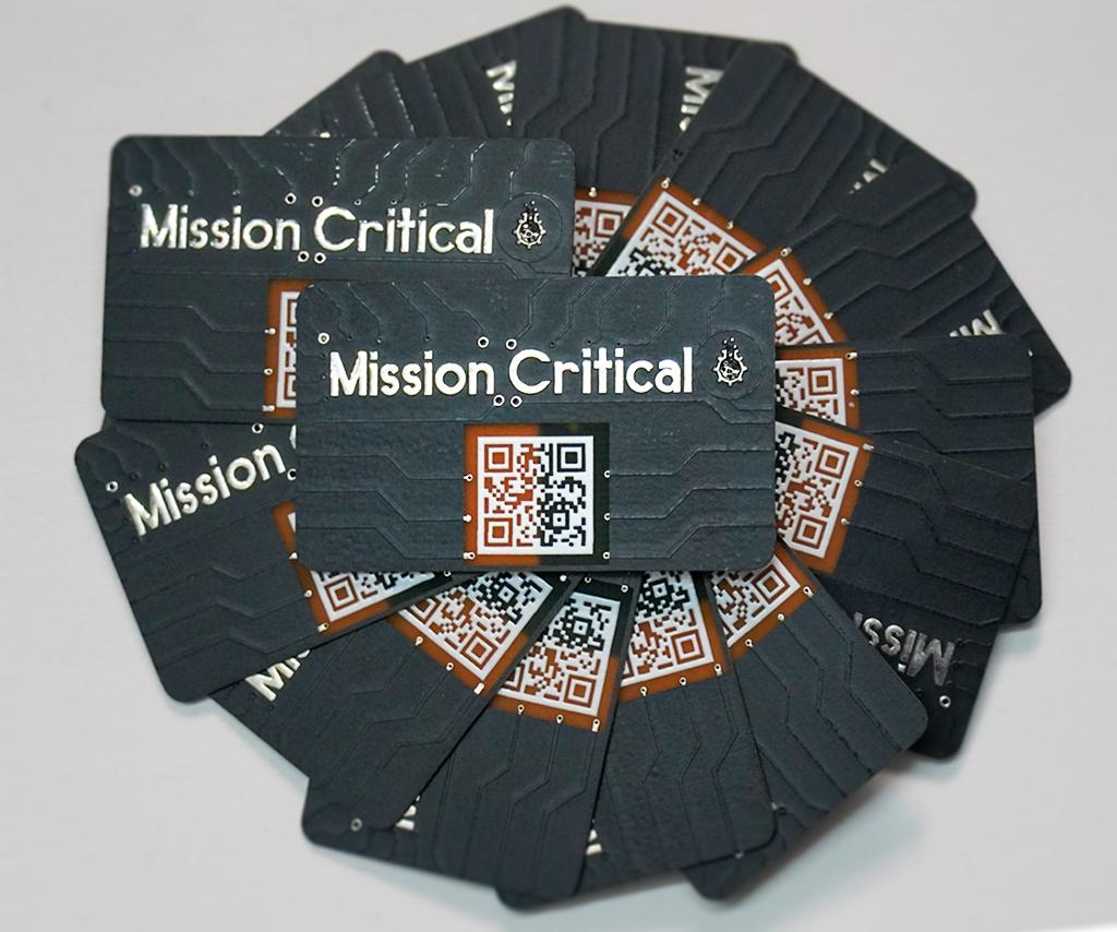

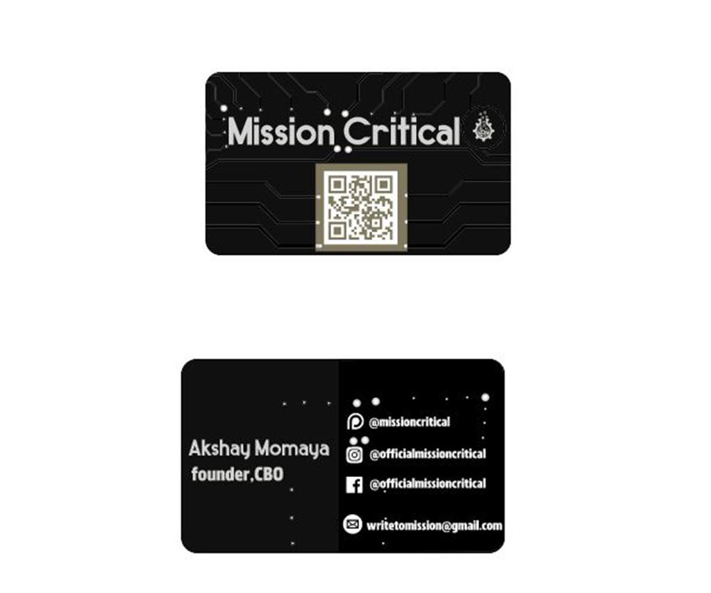
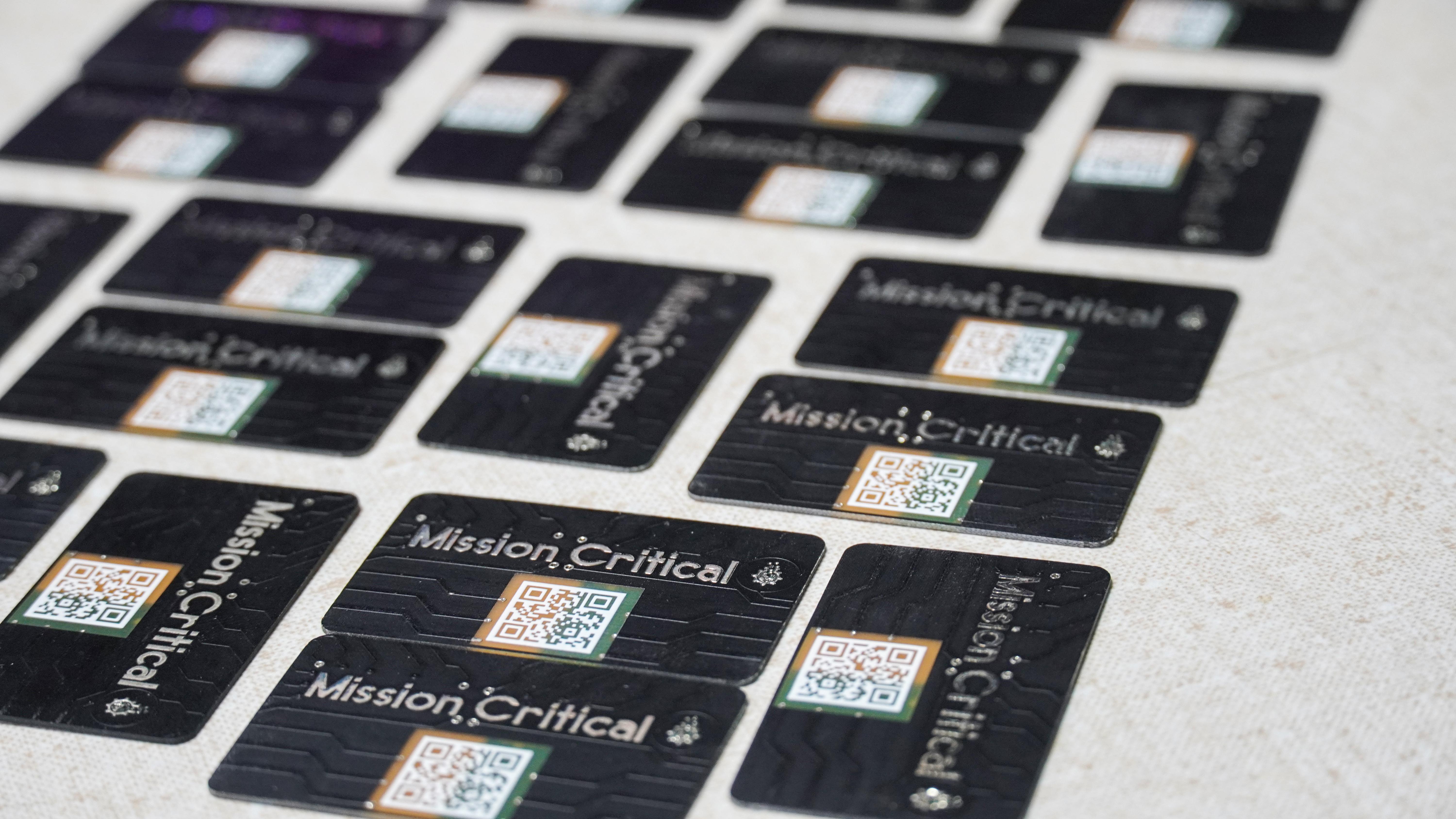
Paper visiting cards are great option for any one, but for Electronic Enthusiasts like you and me its not amusing enough. Today in this blog we will attempt to design and make our own PCB business card or say visiting card. Follow up the end of this blog to learn how I made this super cool yet professional business card!
Supplies
Watch the Video
Creating New Project and PCB
Before we start this project, it is important to brush up few basics of PCB designing, for which you can refer Circuit Board Design class by Randofo also there are 2 amazing posts:
For this project, we are using Easy EDA, but you can use Eagle cad too.
Steps:
- Refer the above mentioned guides to learn PCB designing process.
- Go to www.easyeda.com, register via google account or Email address.
- Create a new project, name it "Business card" ( or anything you like :P).
- Create a new PCB (don't forget to save it.)
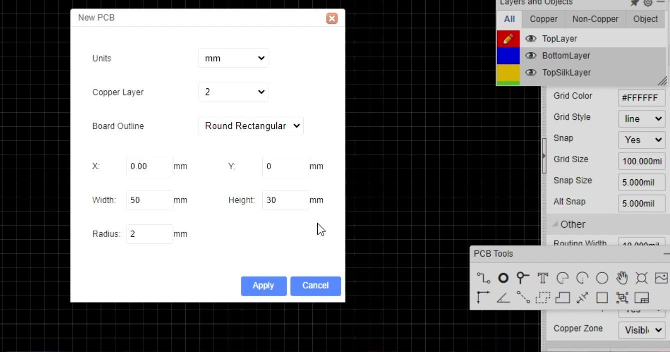
- When asked for board outline select "Round Rectangular", width as 50mm, height as 30mm, XY origin as (0,0) , radius as 2mm (all of these values are according to the size I need, you may change it accordingly).
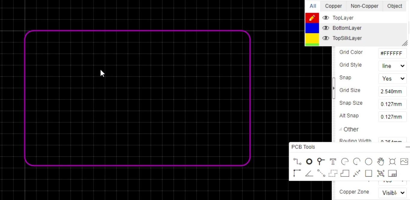
By following the above steps, we have successfully created a Blank PCB board with 50x30mm dimension. The next step would be to design the rest of our Visiting card.
Start With TOP Layer
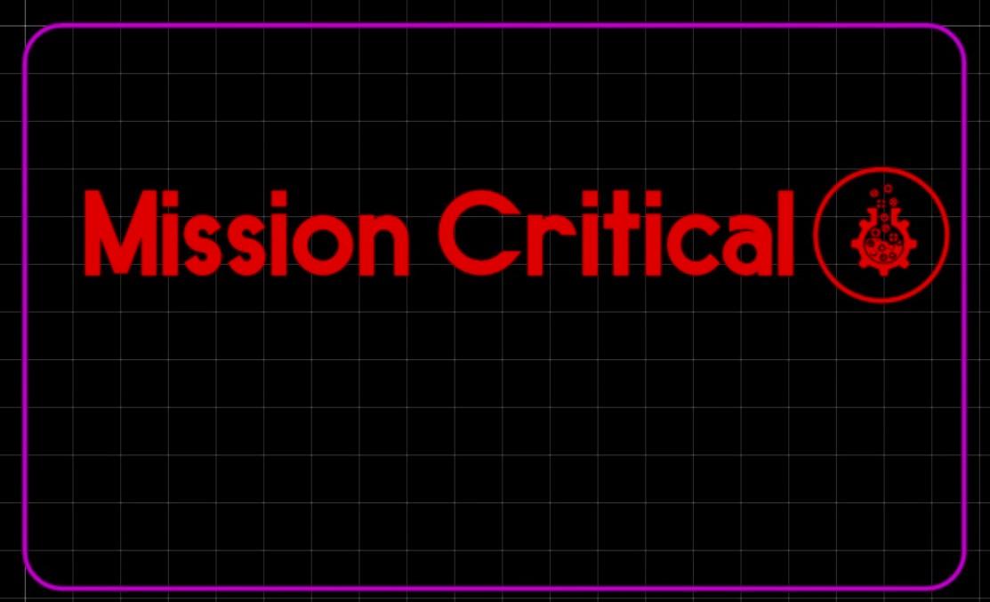
In the last step, we made out Outline for PCB so now we can start with TOP layer.
In TOP layer or say front side, it is a general practice to add Company name and Address. We will do the same by adding "Mission Critical" name and its logo along with Address (since our platform is a digital one, we will add QR code embedding URL inside instead of physical address)
Steps:
- Select the "TopLayer" option on " Layers and Objects " floating submenu.
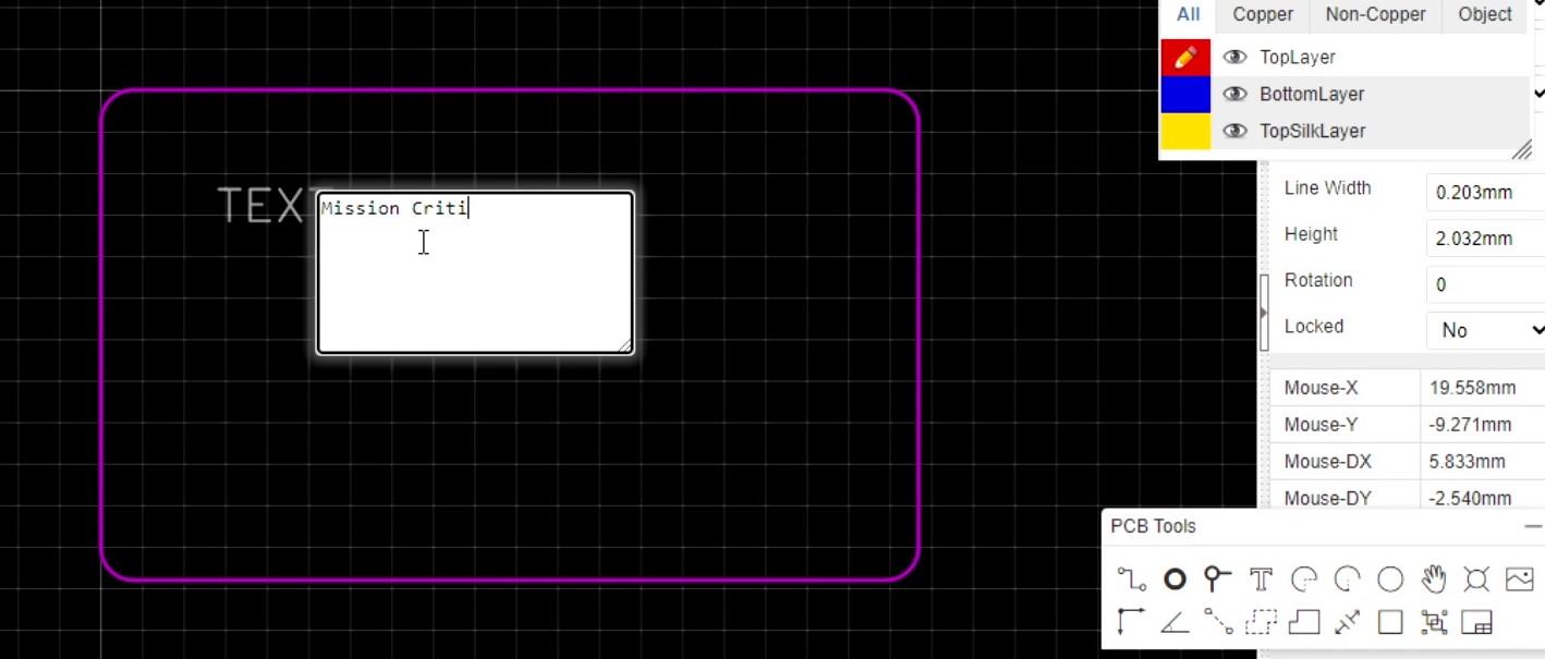
- Select "Text" tool using Shortcut "S" or by selecting "Text tool" from "PCB Tools" floating submenu.
- Enter your company name (or channel name in my case) on the given text, Resize & Adjust it inside PCB outline area. ( Adjust the font to be 6.5mm height)
- Customize the Font via "Font Manager" found on right menu in "Text Manager" Side Menu.
- Upload Desired Font and Adjust until satisfied.
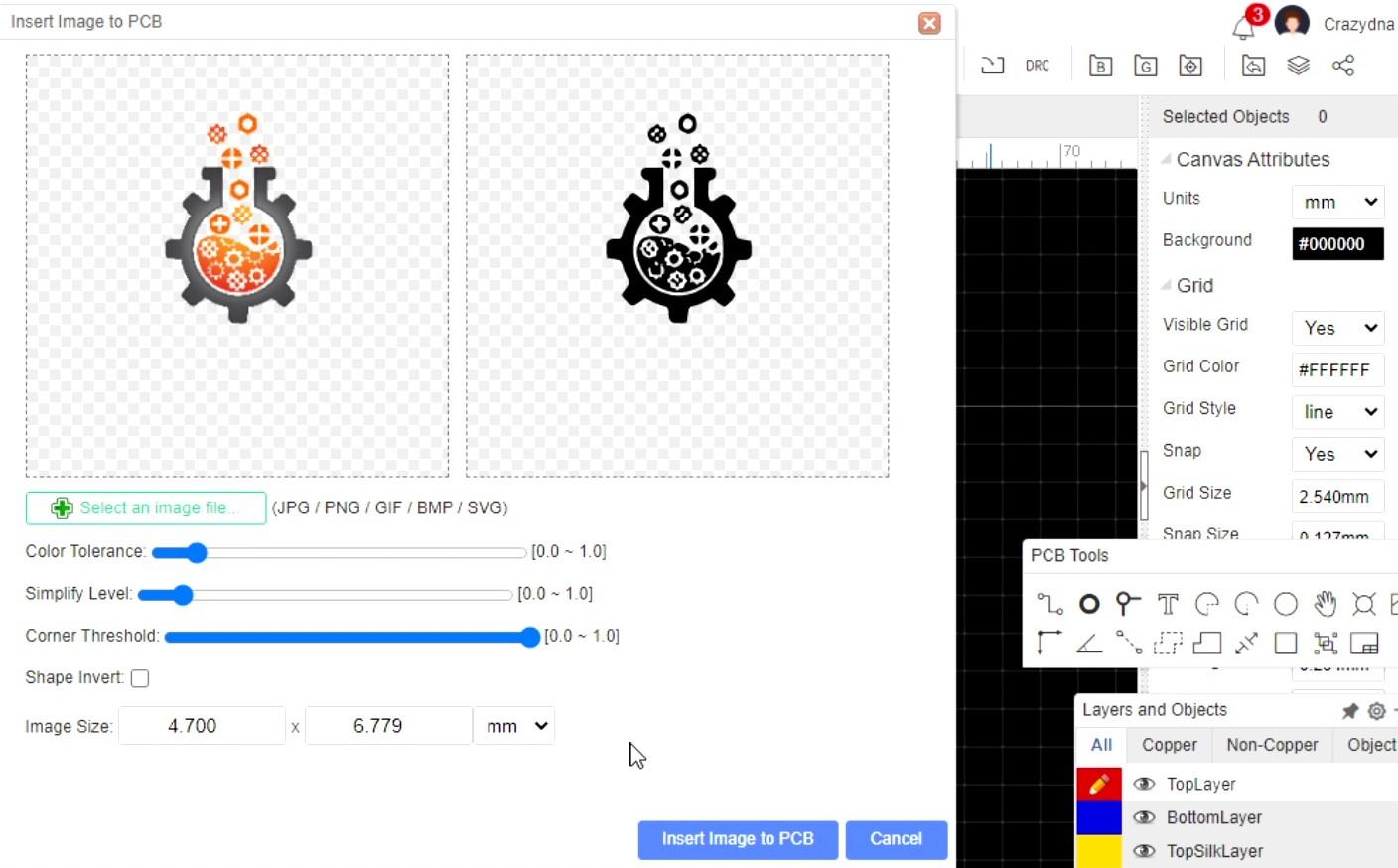
- Select Image tool to upload your Company Logo ( or Channel Logo in my case ) using "Image" tool found in "PCB Tools" floating submenu.
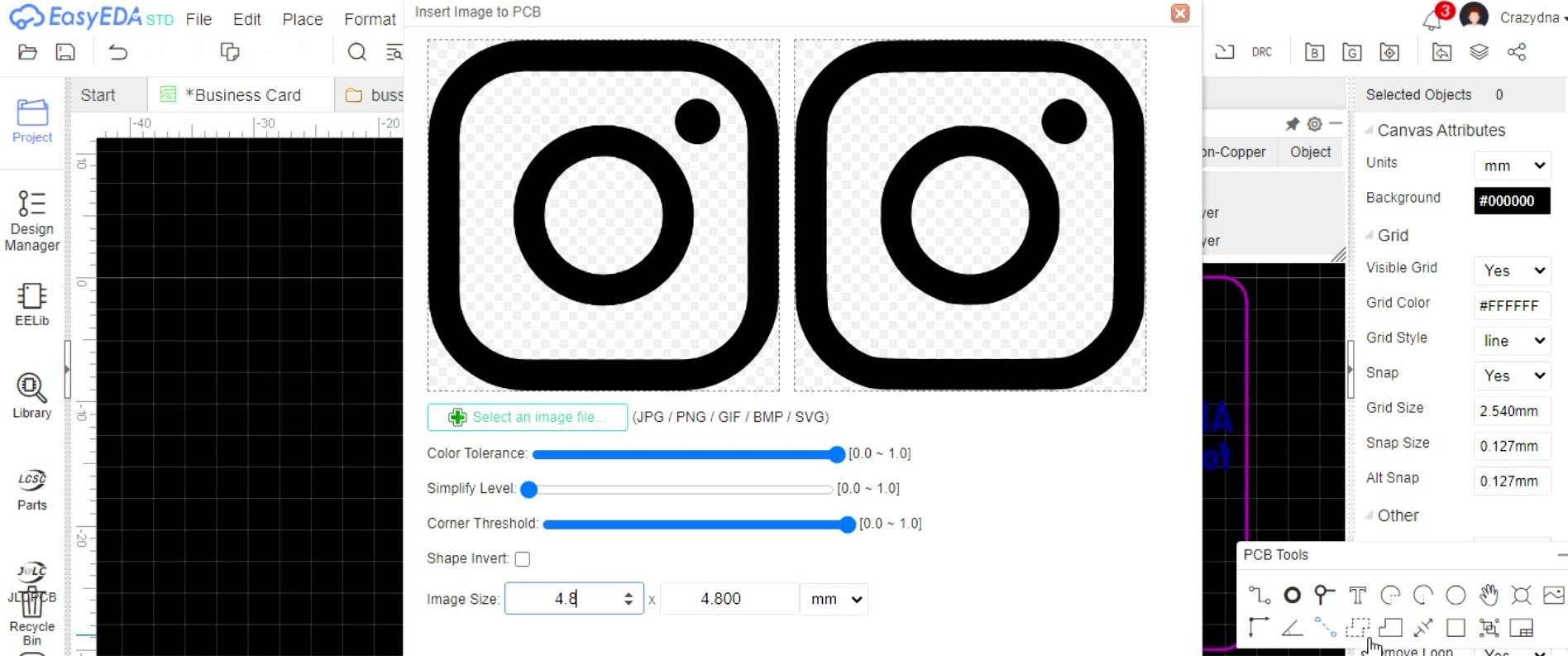
- Browse the Desired Logo by clicking on "Select an Image file" and select the image you want. Adjust the "Color Tolerance" "Simplicity Level" & "Corner Threshold" until you see Desired result in Right ( output ) window. At last, redefine the Image Size to be 5mm ( less or more depending on your Logo).
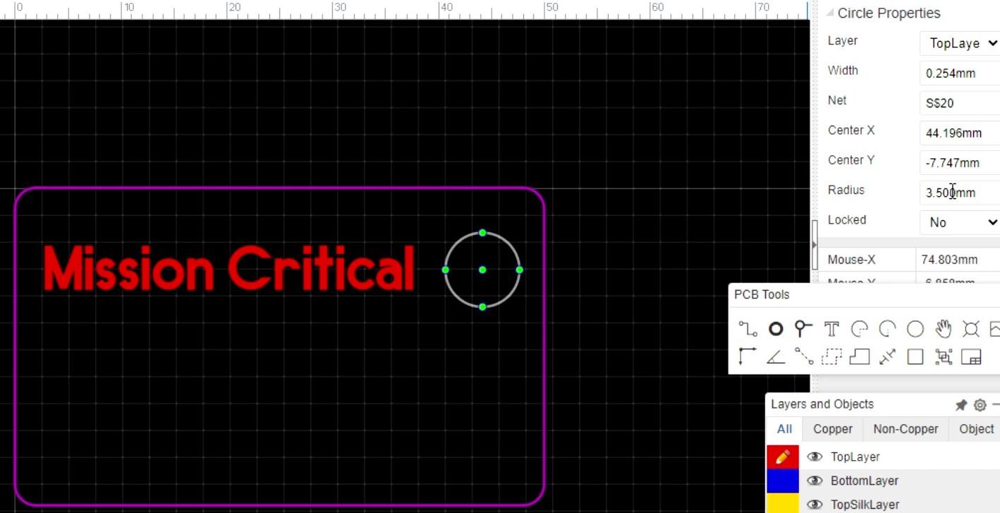
- Draw Circle using "Circle" tool by pressing keyboard shortcut "C" or by selecting "Circle" via "PCB Tools" floating submenu.
- Redefine the Radius of Circle to match the Logo size in "Circle Properties" Side Menu.
Embed QR Code on TOP Layer
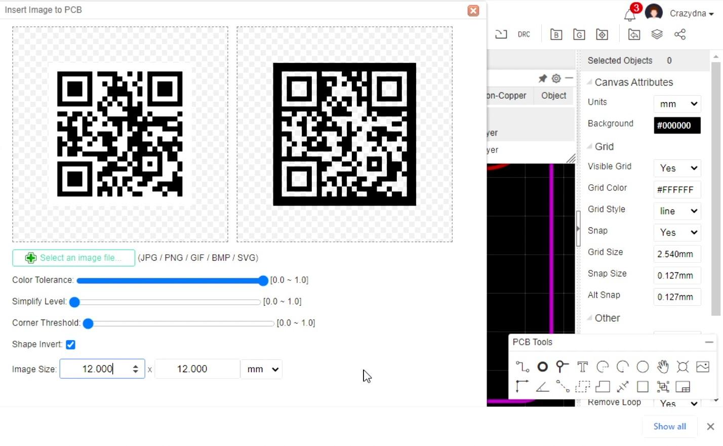
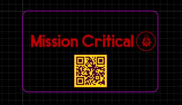
As discussed before our platform is a digital one so we need to add URL instead of physical address.
we can easily Embed URL using QR Code which can later be scanned by anyone to reach your URL or channel or website.
Steps:
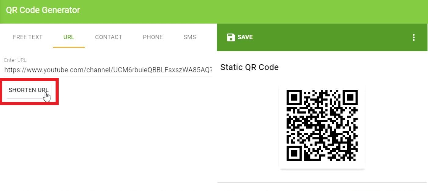
- Go to QR Code Generator website.
- Go to URL section and paste the URL that you need to embed inside the QR code
- Click on shorten URL to make sure complexity of our QR code doesn't get too big.
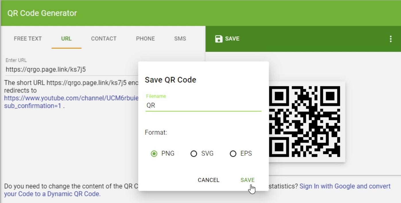
- Download and save QR code as image.
- Using the image tool, add the QR code image saved on your PC
- Click on invert shape button.
- Tune the corner threshold to 0.
- To avoid getting imperfection while manufacturing, we will remove the solder mask layer of the QR code section, for which we will make a square using "Rect" tool on Top solder mask layer.
After this step is done, we can move to backside of card or say Bottom Layer.
Prepare the Bottom Layer
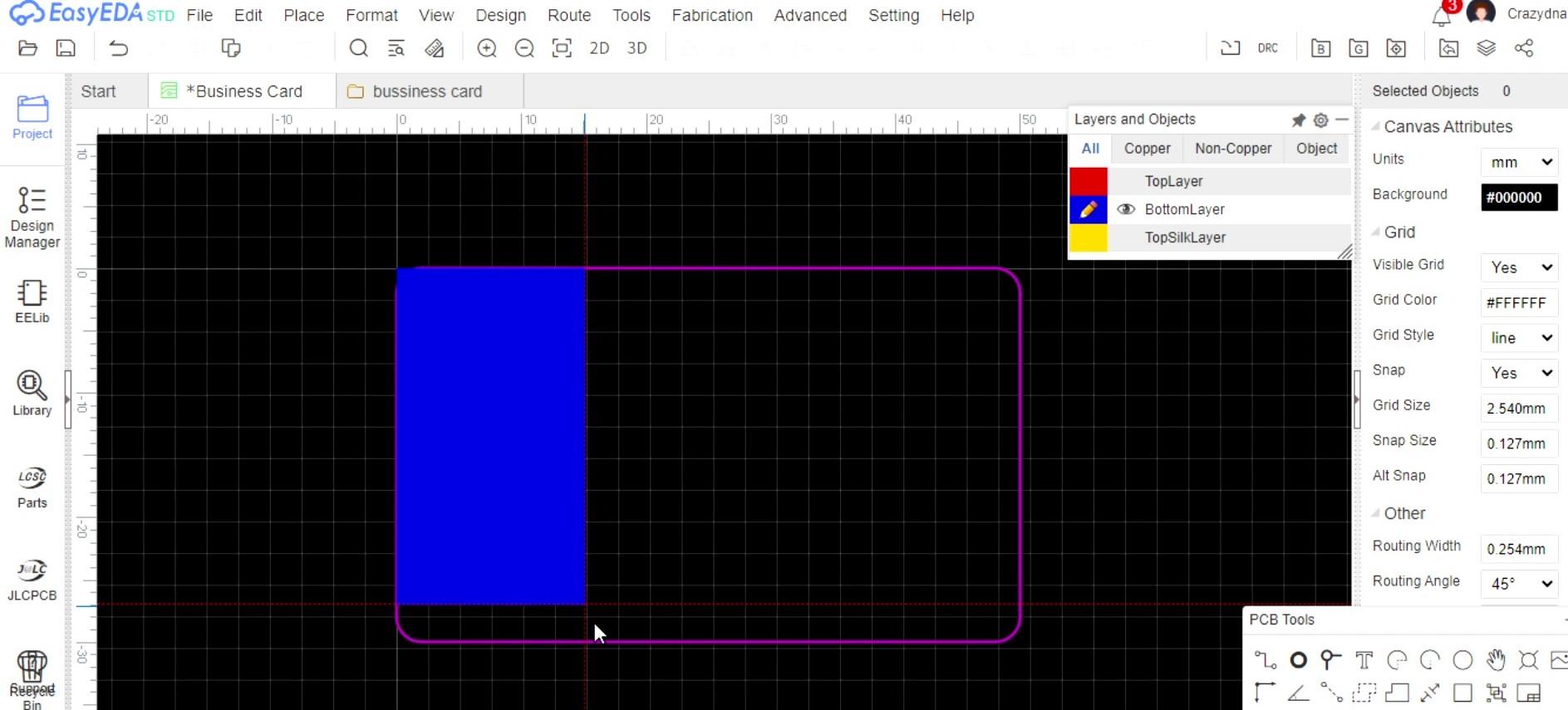
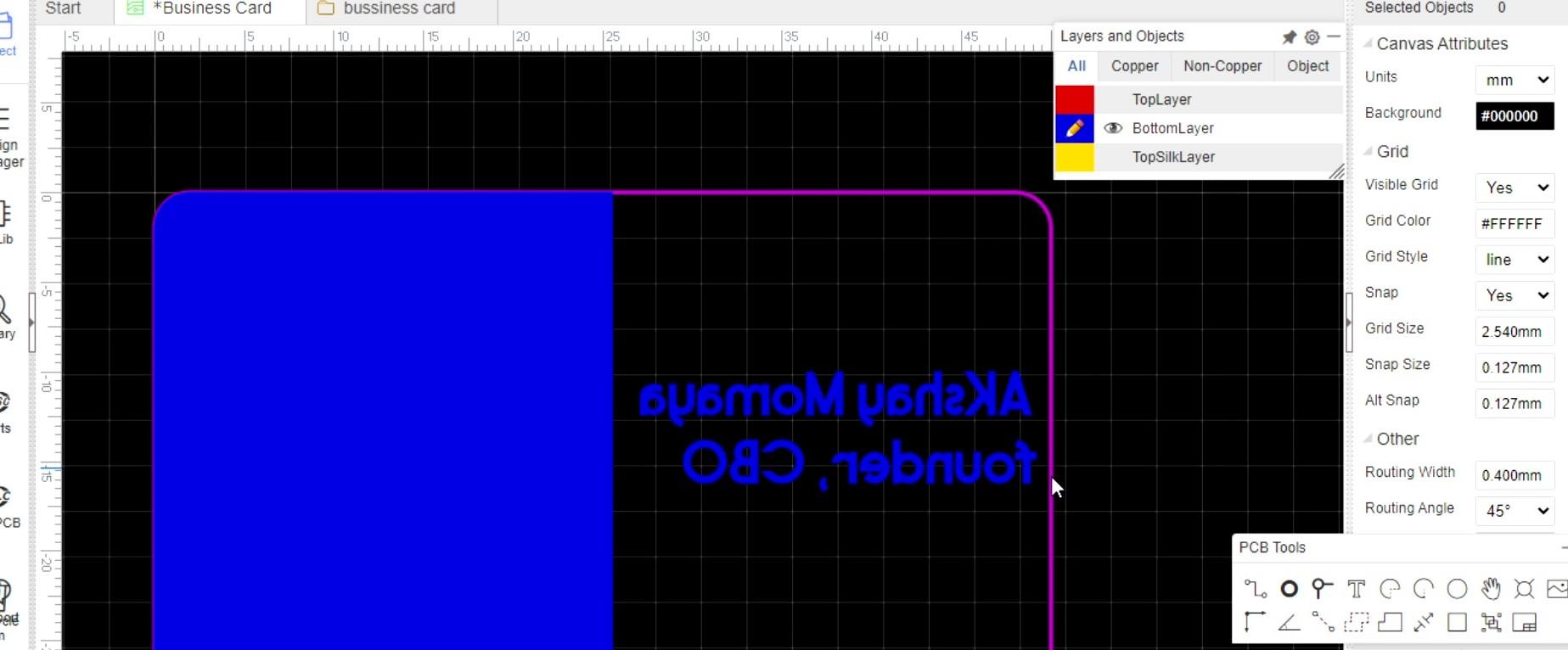
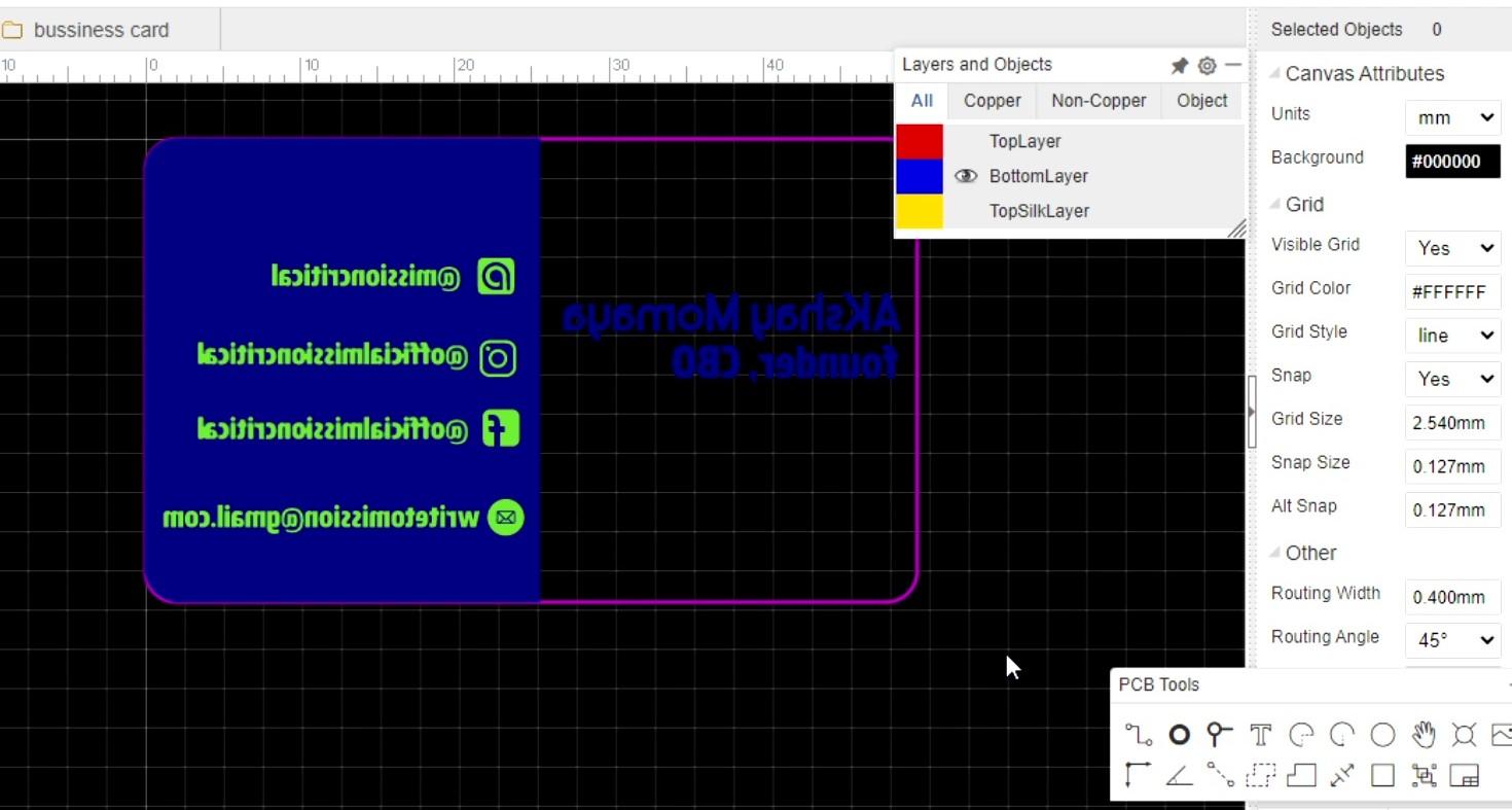
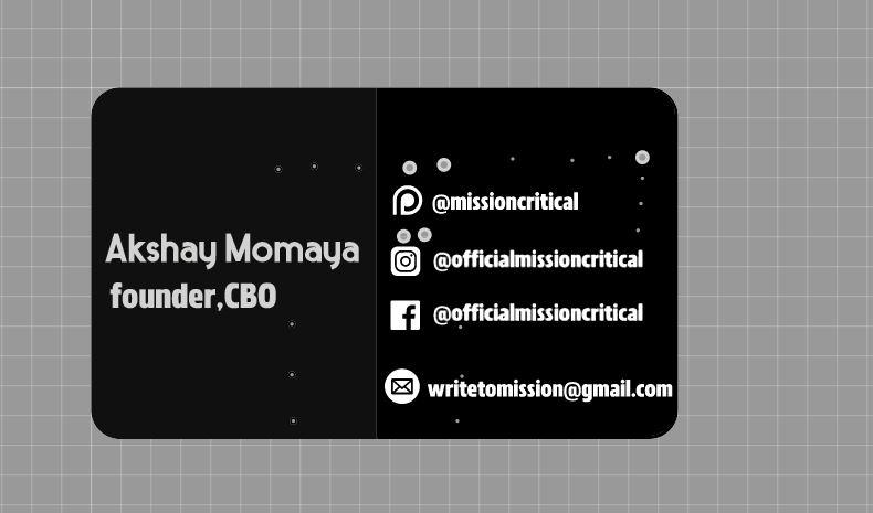
Since our Front layer was Complete, we can proceed to Bottom Layer and divide the back side into 2 separate areas to write all necessary information like social media handles, name and designation.
Steps:
- Select the "BottomLayer" option on " Layers and Objects " floating submenu.
- To divide the backside into 2 parts, we will use "Solid Region" tool covering half region of card.
- To add Name and Designation using "Text" tool or keyboard shortcut "S" or by selecting Text tool via "PCB Tools" floating submenu.
- For social media handles, we will again use Image tool and import social media logos of Patreon, Facebook, Instagram and Email.
- At last we will write user ID of Social Media handles using "Text" tool via "PCB Tools" floating submenu.
- Adjust all the layers to suitable Orientation.
At this stage we are almost done and we can export Gerber file, but i would like to add few things in front or Top layer.
Add Your Accent to This Design
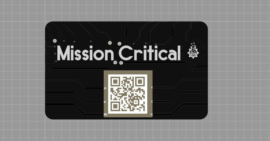
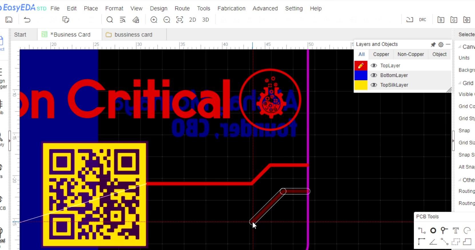
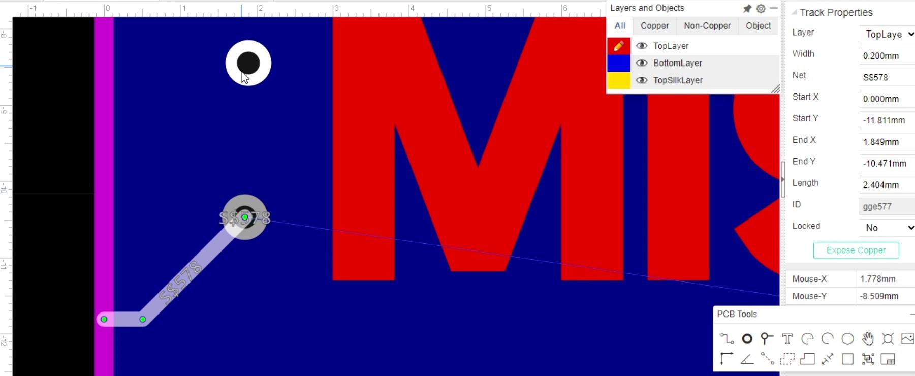
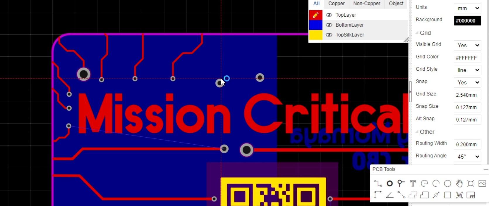
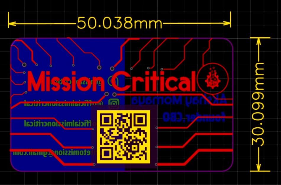
We will add few tracks to make this design look more like a PCB and add our own accent to this card. For which we can use Vias and Holes of various sizes also add few tracks of various sizes until satisfied with the end result.
Steps:
- Go to the "TopLayer" option on " Layers and Objects " floating submenu.
- Plot Via holes near Company name and QR Box using "Via" tool in "PCB Tools" floating submenu or by using keyboard shortcut "V".
- Plot holes near any region using "Pad" tool in "PCB Tools" floating submenu or by using keyboard shortcut "P".
- Make Tracks according to your Creativity using "Track" option in "Layers and Objects" Floating submenu or by using keyboard shortcut "W".
- Redefine the width of tracks to create texture in PCB using "Track Properties" which is located in Side Menu.
You can add or subtract any element from this step and make it truly unique by introducing your own creativity in this step!
Once satisfied, we can check out render file ( preview ) in " View" menu and "2D view" or "3D View" submenu to see how our PCB will look.
Render Gerber Files and Place Order
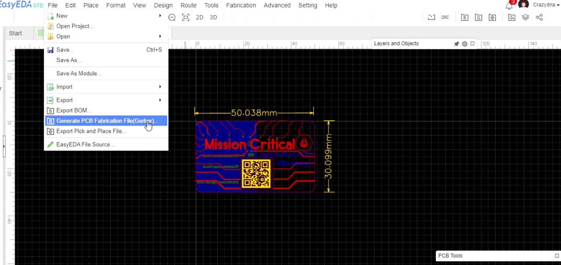
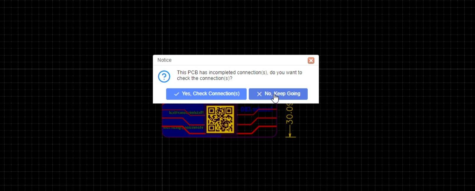
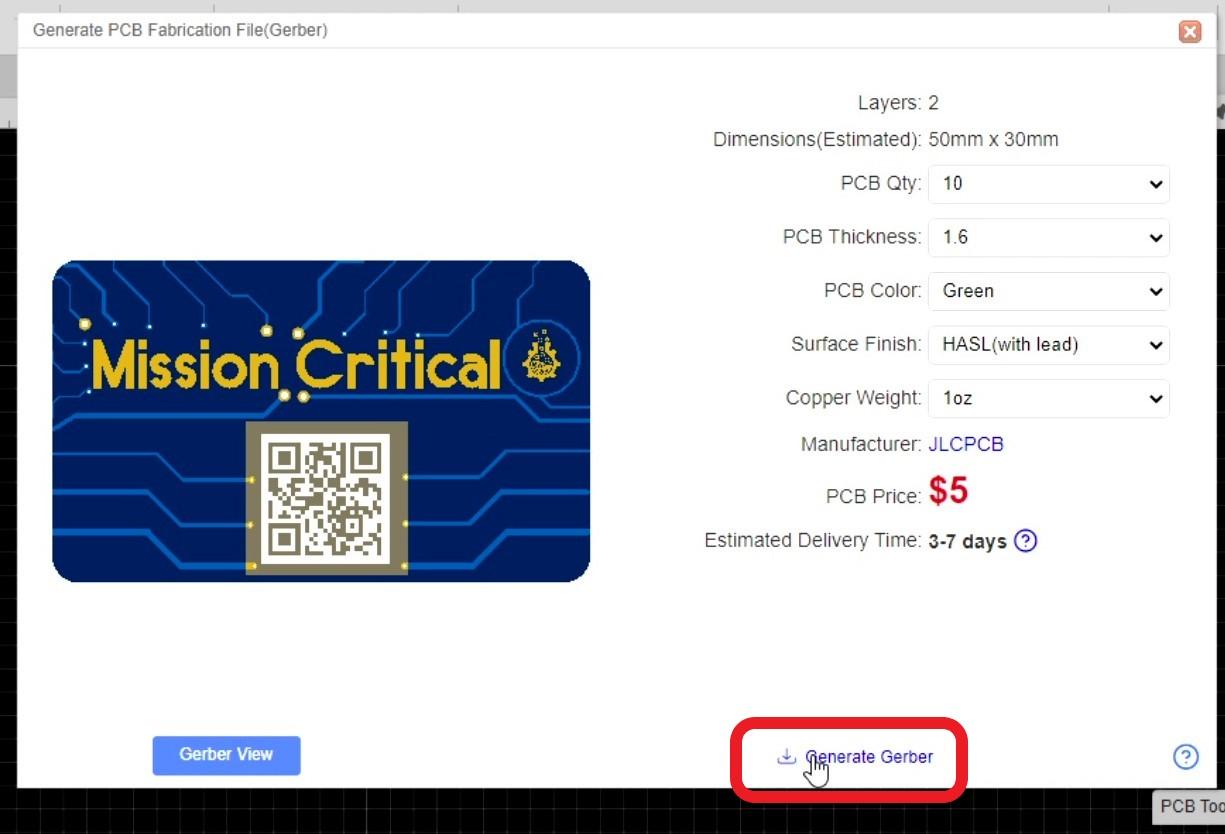
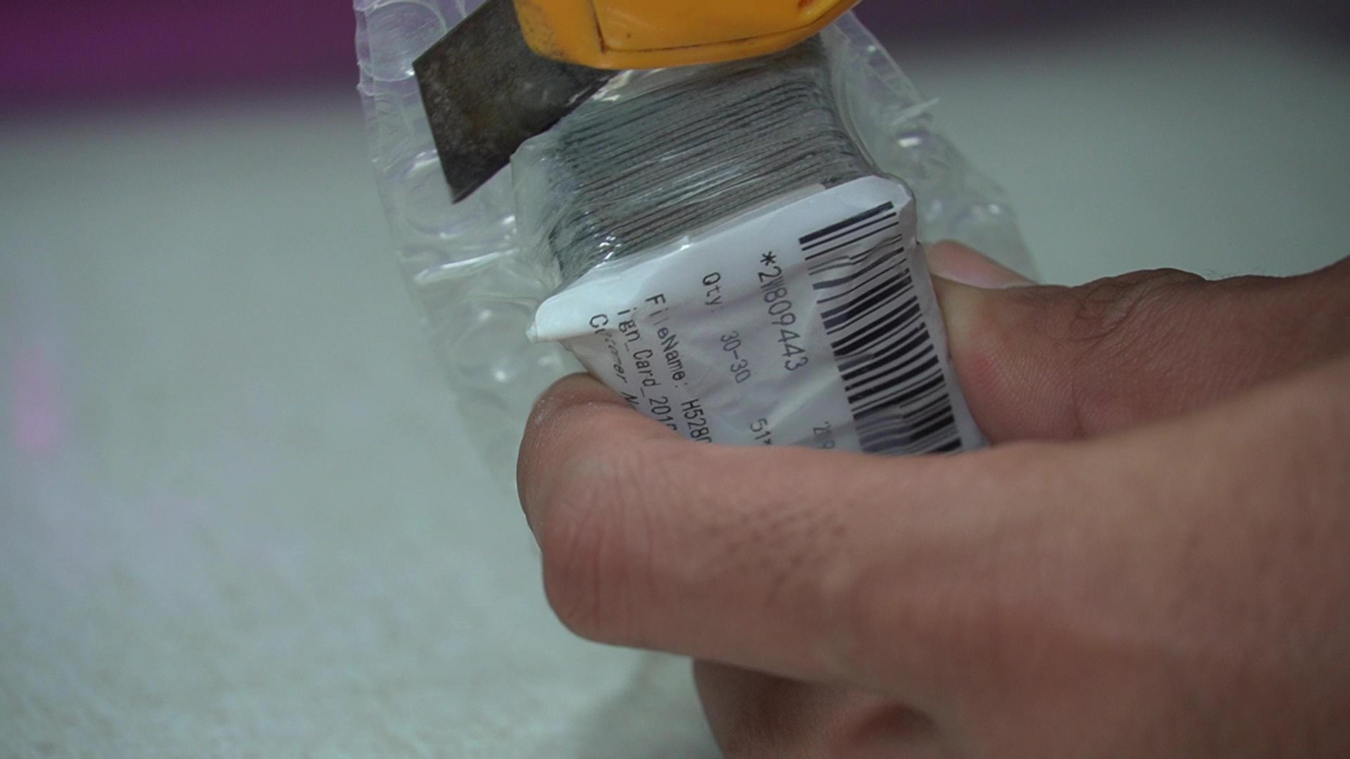
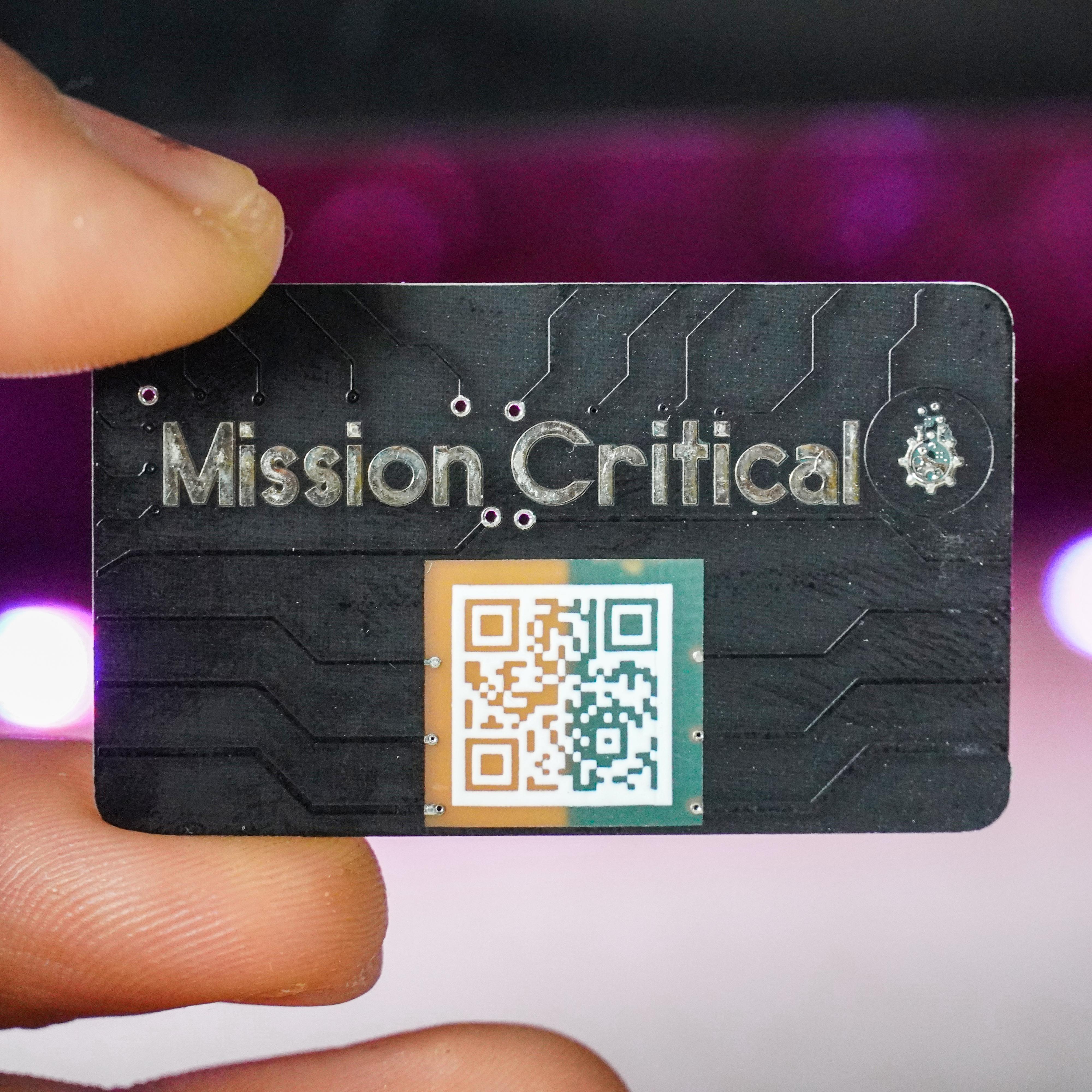
Once our Design is ready, we can Generate the Gerber file and send it for manufacturing to any PCB manufacturer.
Steps:
- Go to files menu and generate "PCB fabrication file or gerber" option.
- It will ask if you want to check connections, click on "No, Keep Going" option.
- It will ask for DRC check, click on NO and generate Gerber.
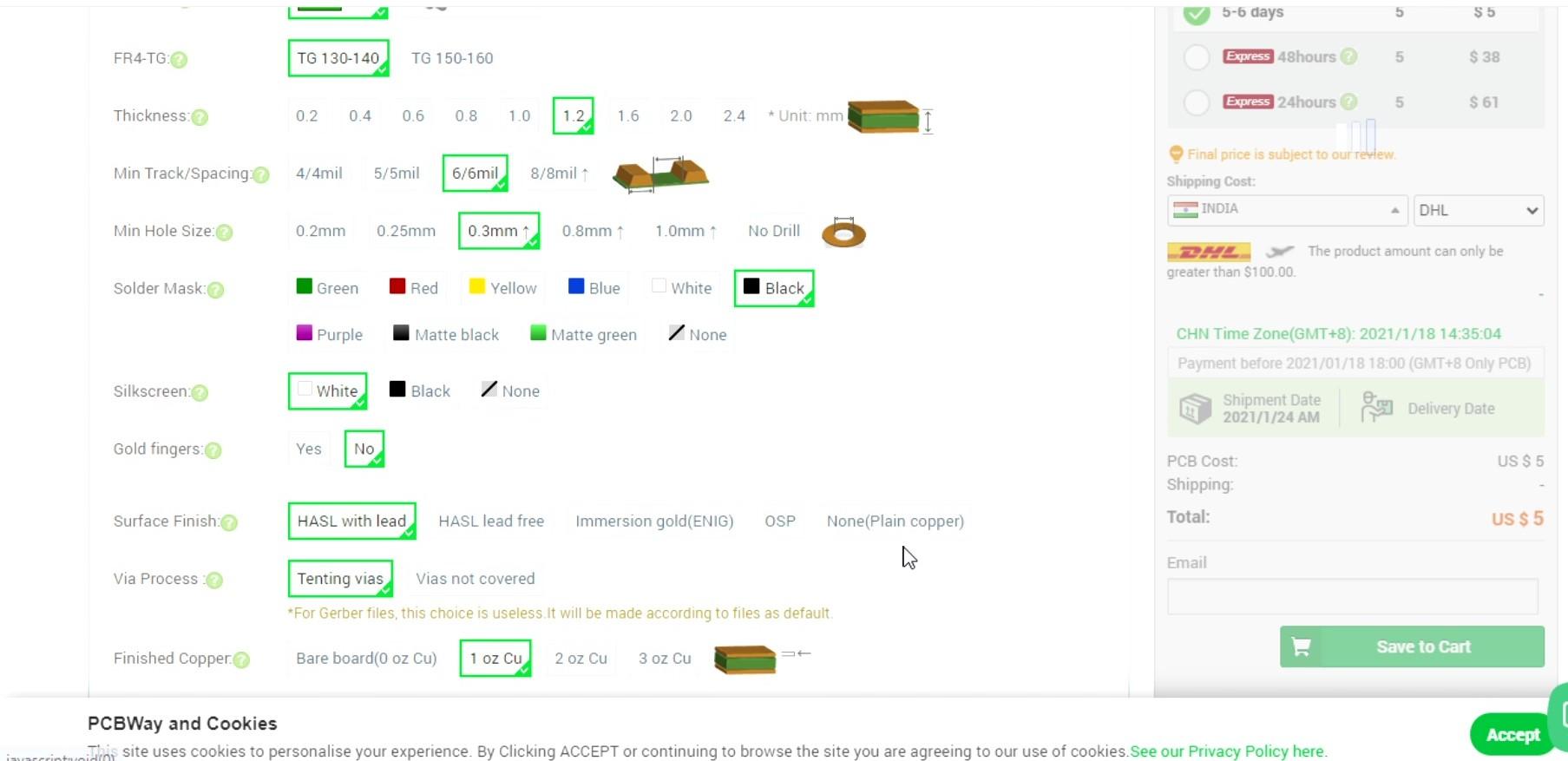
Now to order this PCB, go to any PCB manufacturer, the parameters for Ordering PCB will be standard other than:
- Quantity - 5/10.
- PCB thickness 0.8mm.
- Solder mask color - Black.
- Dimension of PCB - Height 30mm X Width 50m.
Once all parameters are set, Order the PCB and wait for it to be delivered.
Done!
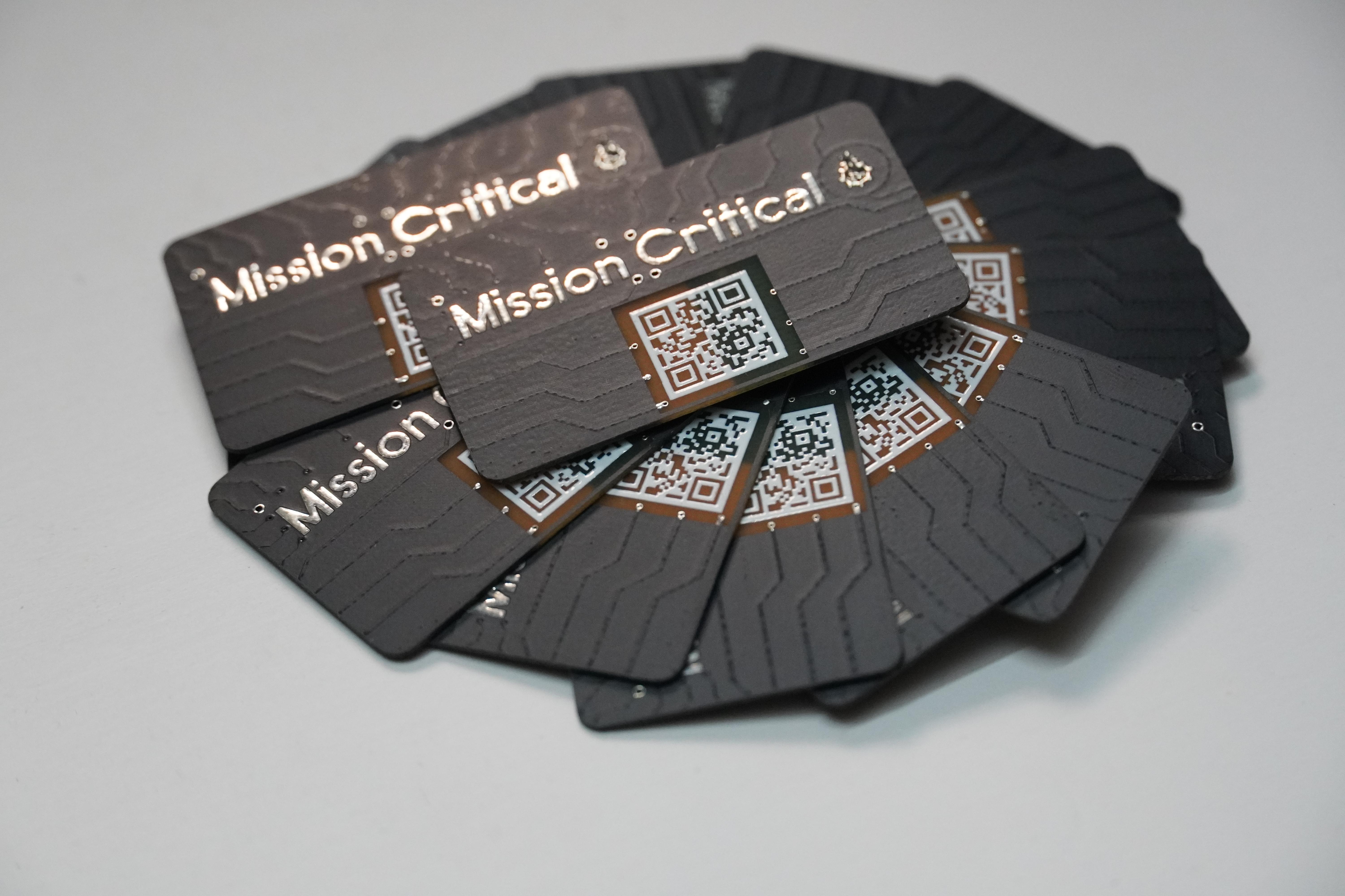
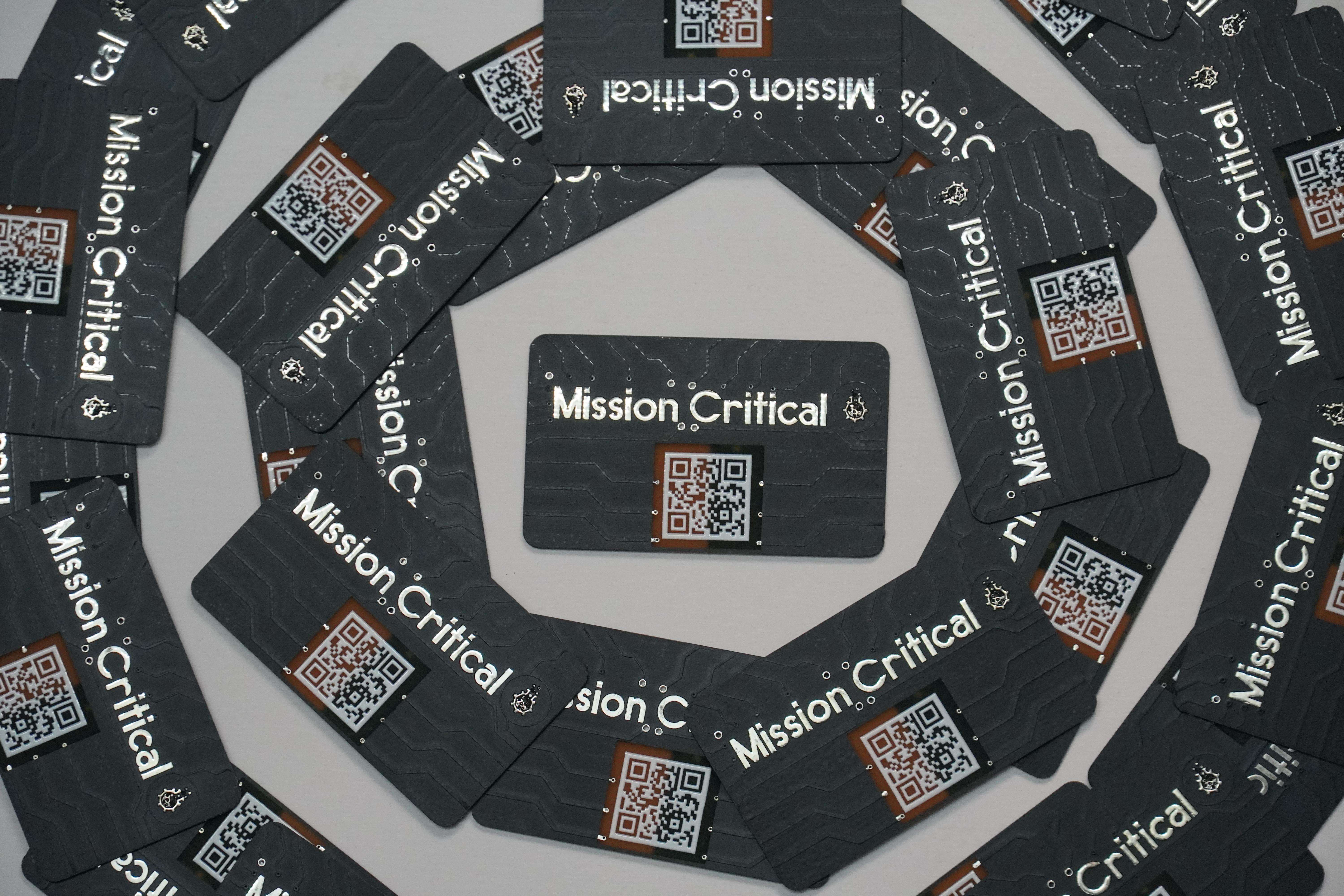
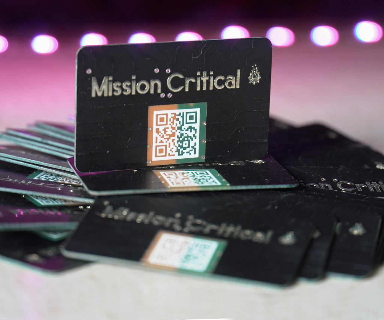
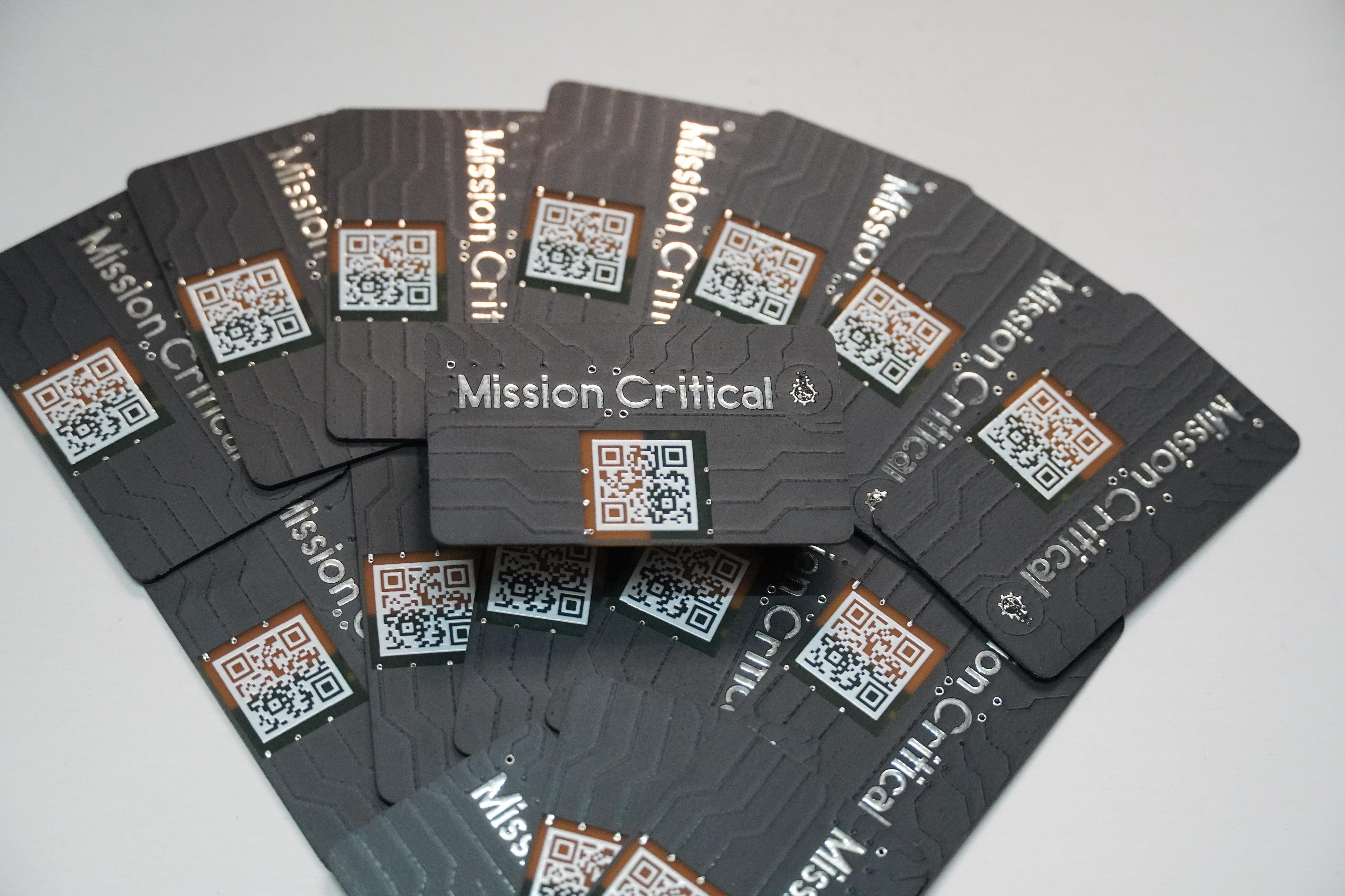
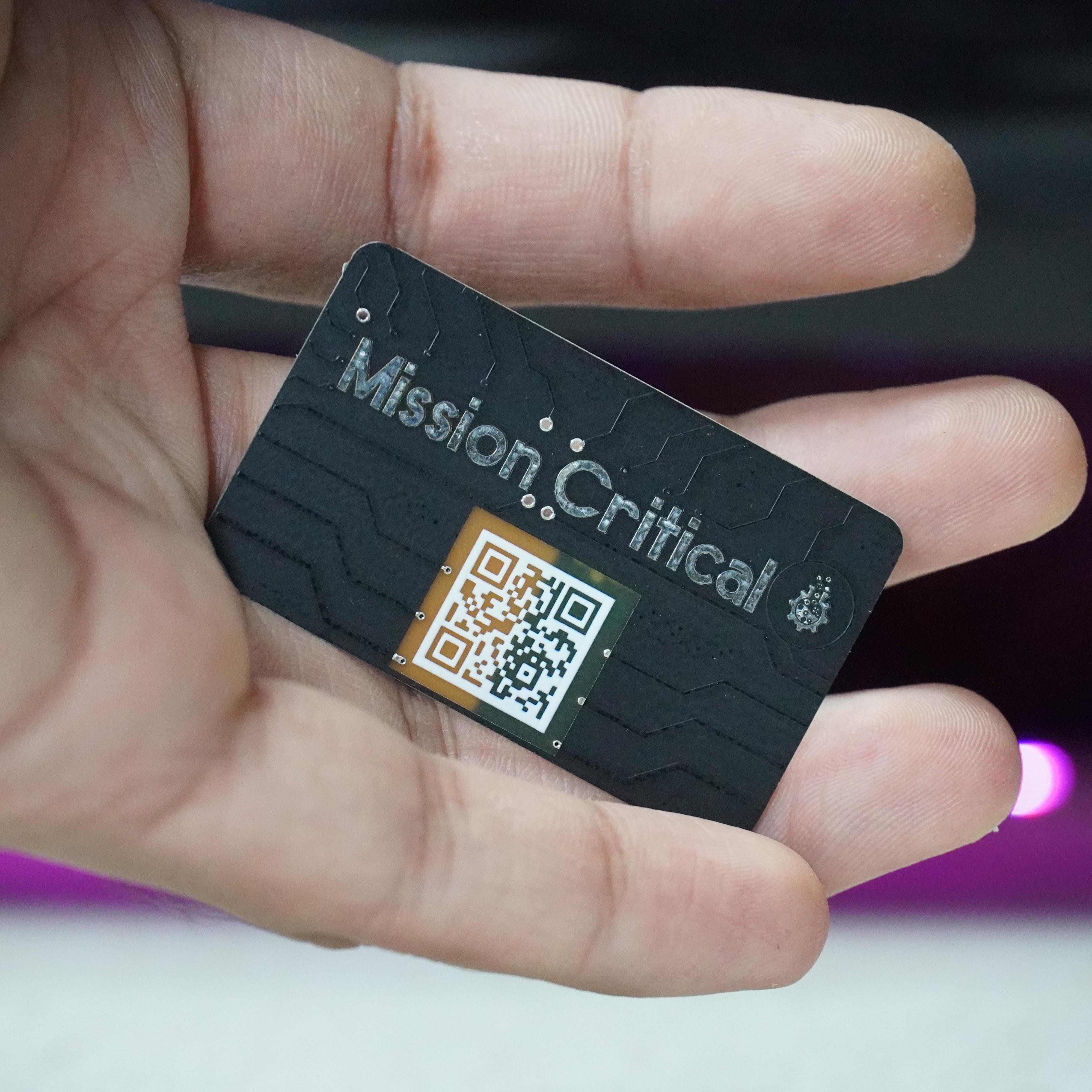
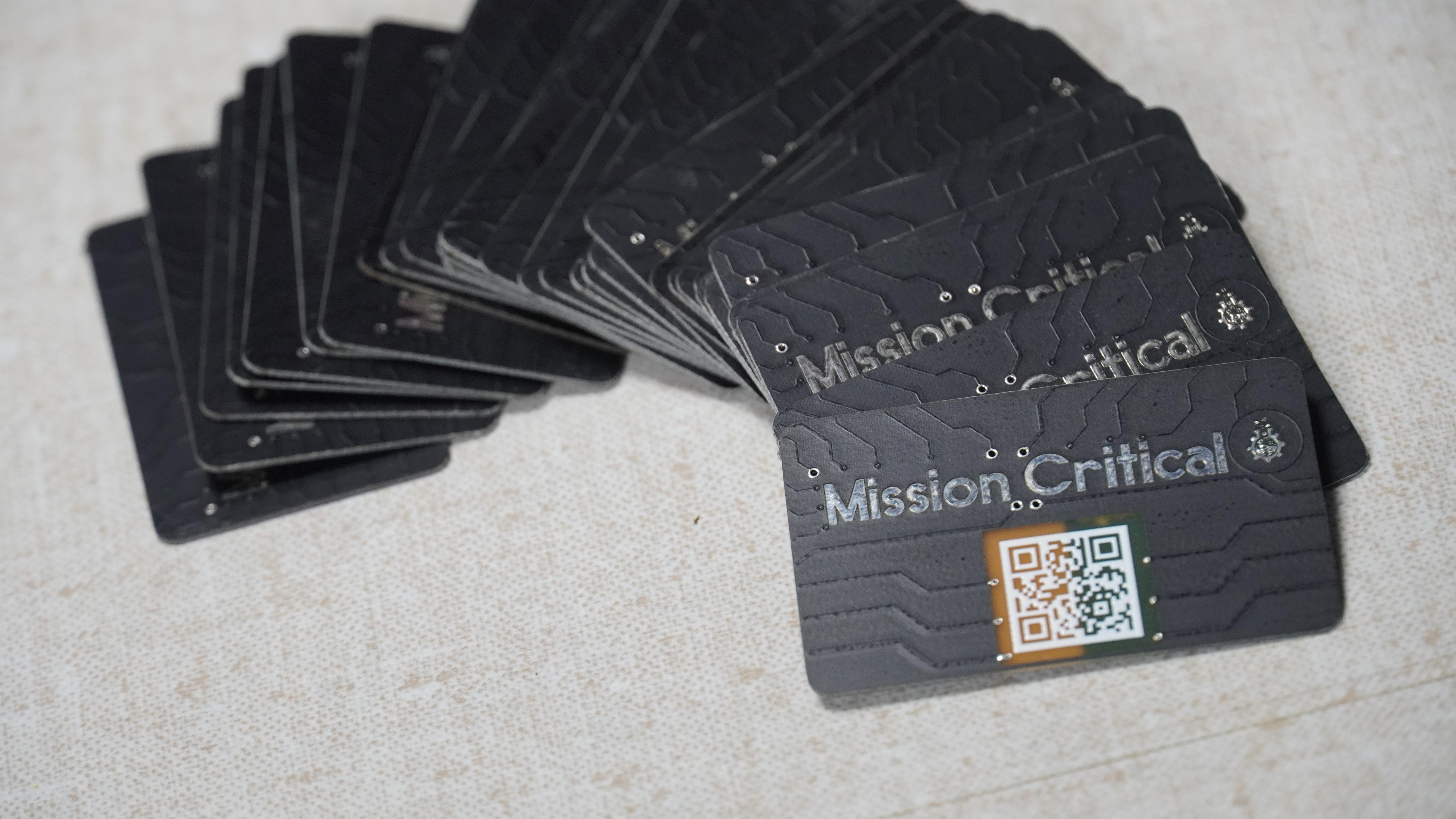
Congratulations, we have made it to the end of this post and learnt how we can easily make a PCB visiting Card. As an engineer this project was a learning curve and looking at end result, we get a satisfying feel. I hope you guys learnt something from this Blog and hopefully reading it.
If you enjoyed this blog post or project, consider supporting our work by subscribing to our YouTube channel and following our Social media handles, your support means a lot to us and motivates us to keep making awesome content!
Social Media Handles: Patreon, Twitter, Instagram, Facebook.
With that being said, I will see you guys in next project, until that keep learning and stay safe! goodbye :)
[ Also we have participated in PCB Challenge, if you like this post, support us by voting! ]