PCB Reverse Engineering Using GIMP
by mjm2008 in Circuits > Electronics
7004 Views, 29 Favorites, 0 Comments
PCB Reverse Engineering Using GIMP


There are only few articles or guides that shows how you can reverse engineer a PCB using a jpg or png picture that you have or you take for a PCB. I tried the one mentioned on this site, but I didn't success in that.
The aim of reverse engineering are many.. I am not responsible for using this technique to do illegal copy of products. My aim is to allow engineers to analyze products by reproducingThere are only a few articles or guides available that demonstrate how to reverse engineer a PCB using a JPG or PNG picture. I have tried the method mentioned on a particular website, but I was not successful.
The purpose of reverse engineering can vary. It is important to note that I am not endorsing the use of this technique for illegal copying of products. My aim is to enable engineers to analyze products by reproducing and studying their circuitry.
Tools required:
- GIMP
- Camera
- Time :)
- KiCad or any other PCB software
Please note that my brushes are provided free of charge, but you use them at your own risk. I cannot be held responsible for any damage or issues you may encounter while using these files.
Downloads
Preparation and the Actual Reverse Engineering
Here's a step-by-step guide:
- Extract the file into your GIMP brush folder. Different folders allow you to filter the brushes in GIMP 2.8.2 as needed. Feel free to remove or add more brushes.
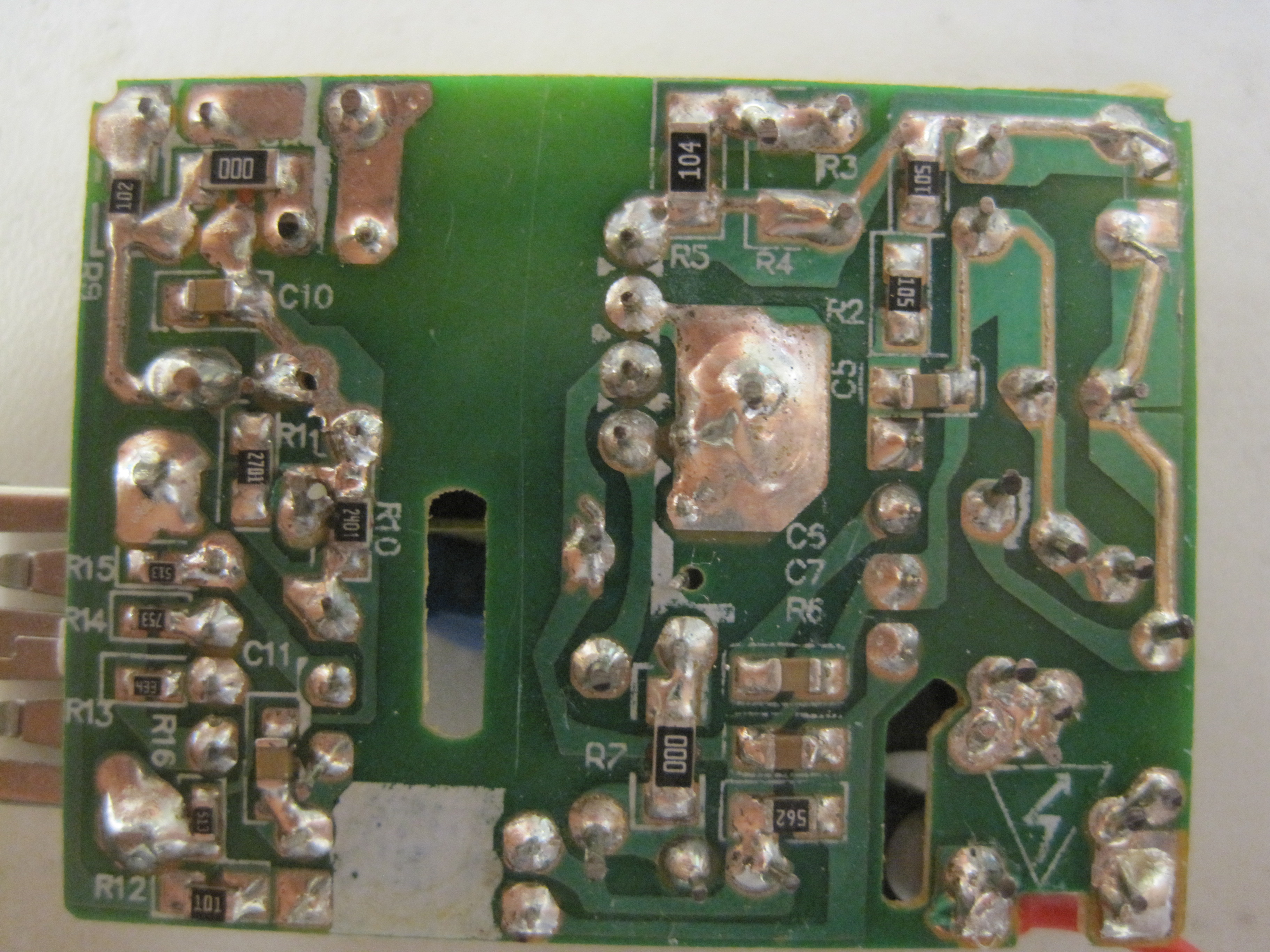
- Begin by aligning the PCB in GIMP and removing any artwork or paint present on the PCB.
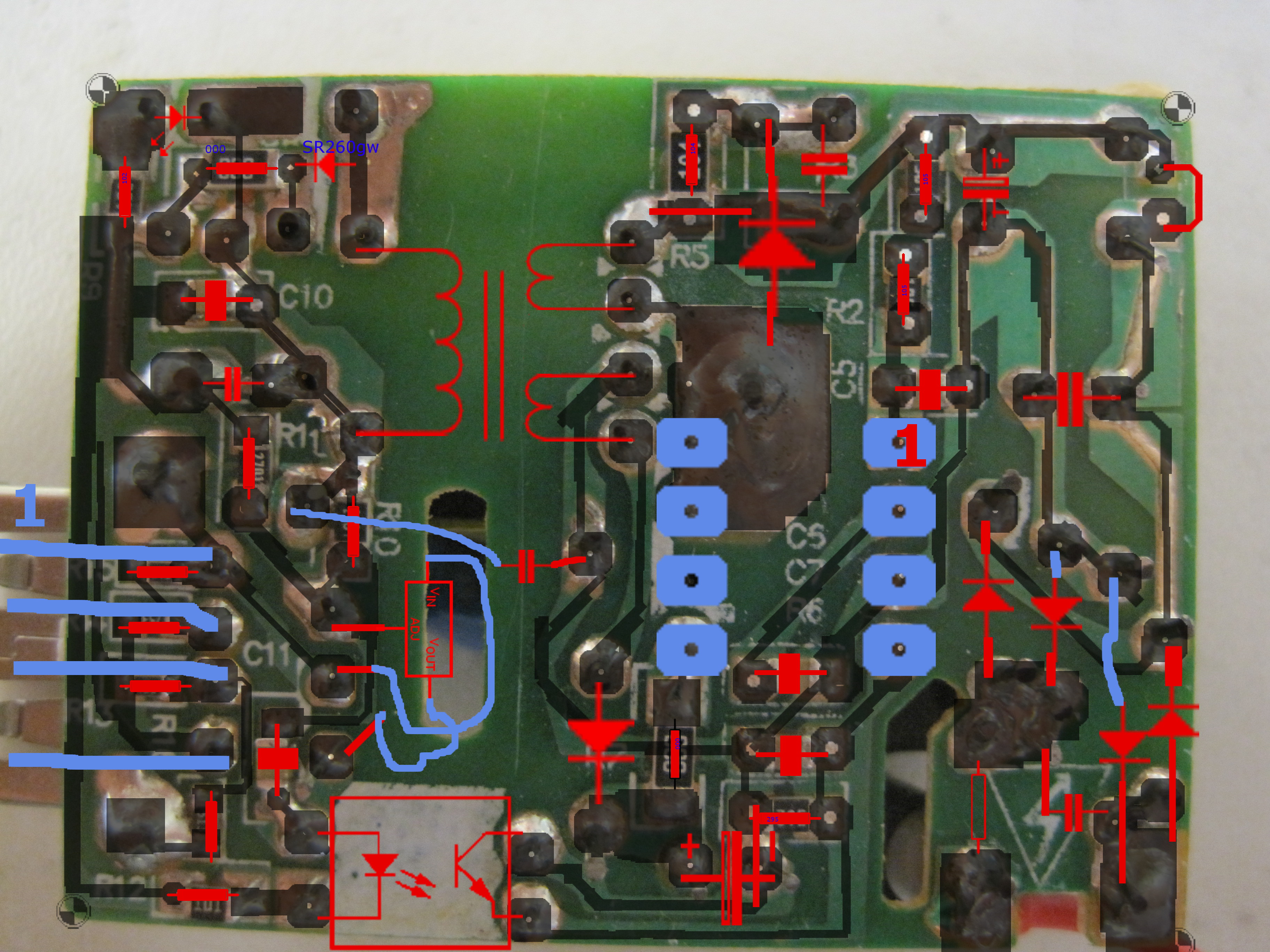
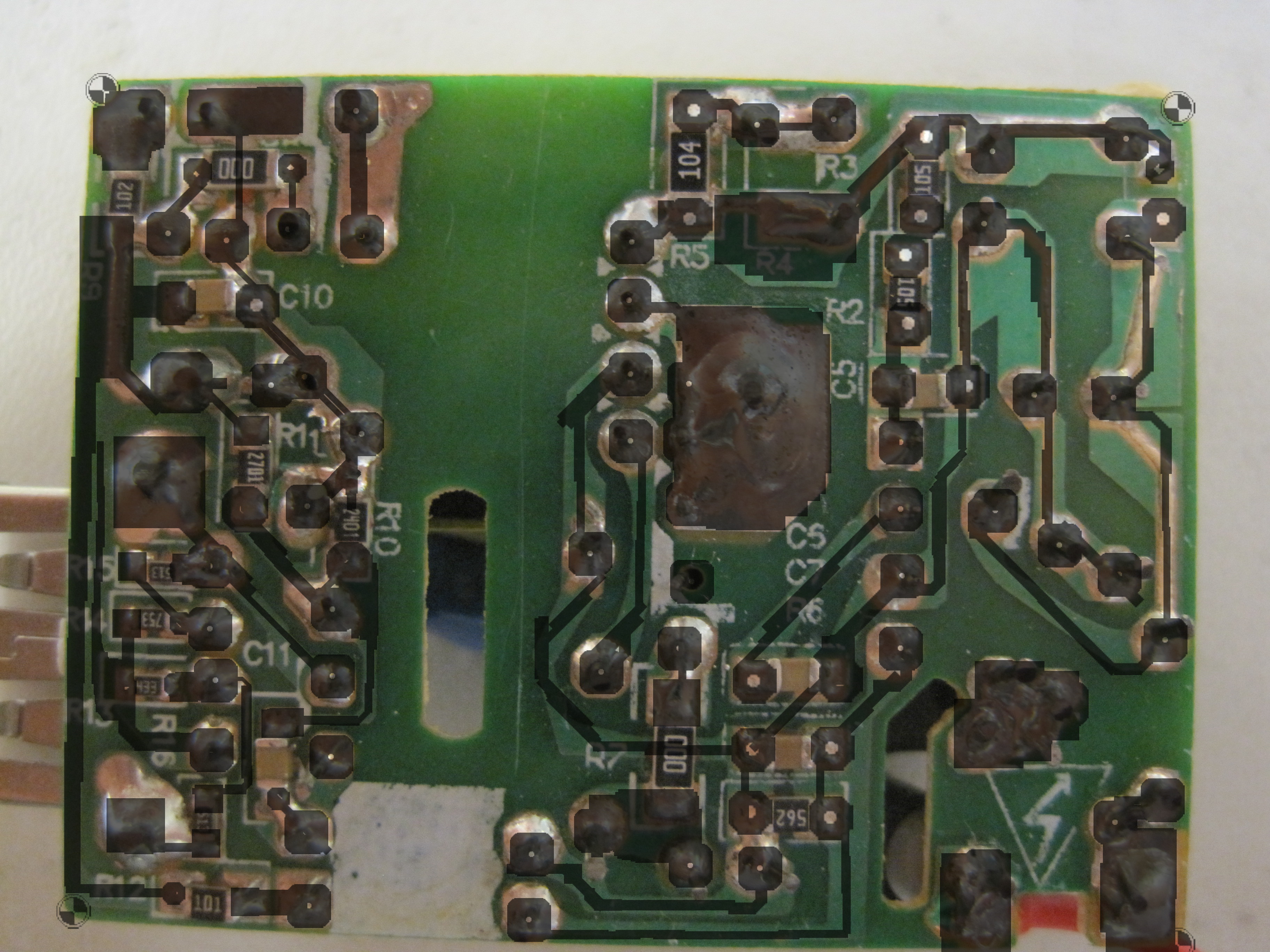
- Create a separate layer for each task. Start with a layer for the connectors, using a black color with 50% opacity to make the tracks visible in the picture.
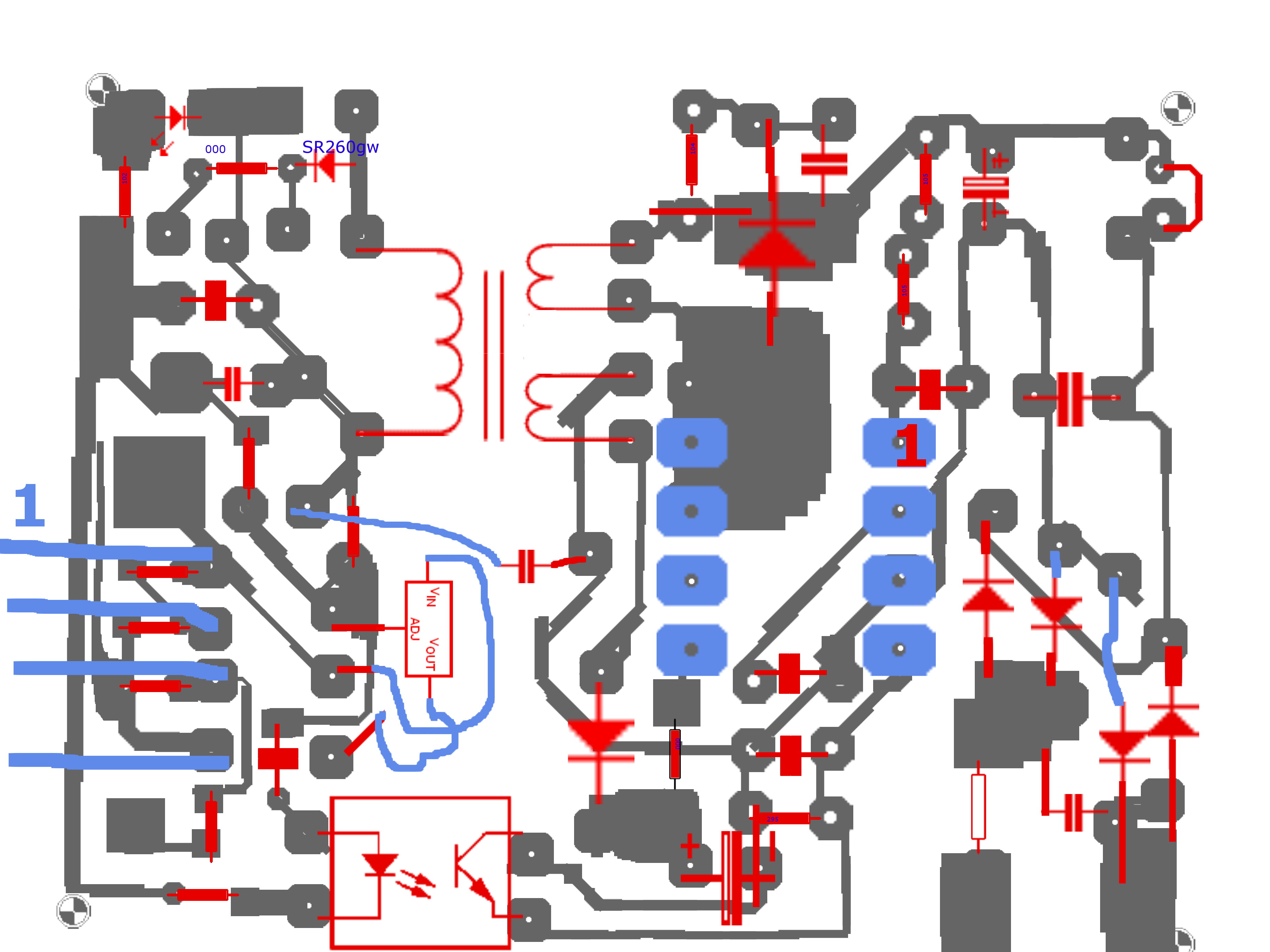
- Create another layer for the components and use a different color. First, place the components located on the bottom side of the PCB.
- Create yet another layer for the components, using a different color. Select the required components, and if the correct chip brush is not included in the RAR file, create a brush by modifying the existing ones.
- Import or open the front (top) side of the PCB, and flip it to match the bottom side. Try to draw the components you find.
- Utilize the eye button to show or hide any layer.
- After completing the drawing, review it and save your files every time you make changes.
- Use descriptive names for each layer.
- Once you have finished your drawing, open KiCad and recreate the components and connectors exactly as they appear in the GIMP project. Do not attempt to move the components or connectors in KiCad at this stage. Keep the layout the same as in GIMP.
- After completing the drawing in KiCad, make a copy and begin rearranging the components and tracks to create a clear schematic.
That's it!
This method provides an easy, quick, and effective way to reverse engineer a PCB. I hope you find this information useful. Please let me know if you like the idea.
Mariwan Jalal