PCB Manufacturing Exporting Process
by depoi120309 in Circuits > Electronics
411 Views, 2 Favorites, 0 Comments
PCB Manufacturing Exporting Process
This is a detailed explanation and guide to how to design and manufacture a PCB from a circuit on Tinkercad to export to be made by the company JLC using Fusion 360.
Supplies


Uploading Your Circuit Onto Fusion 360: 1
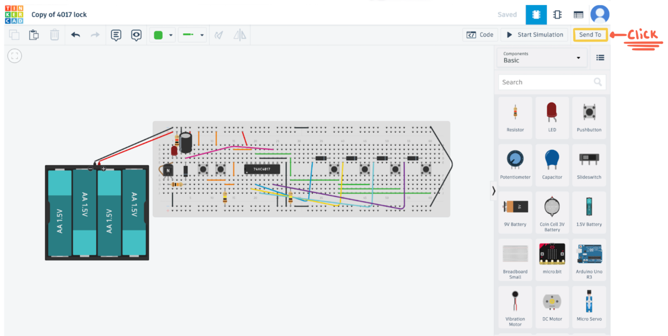
After you have created a functioning circuit in Tinkercard, click on the SEND TO button in the upper right-hand corner.
Uploading Your Circuit Onto Fusion 360: 2
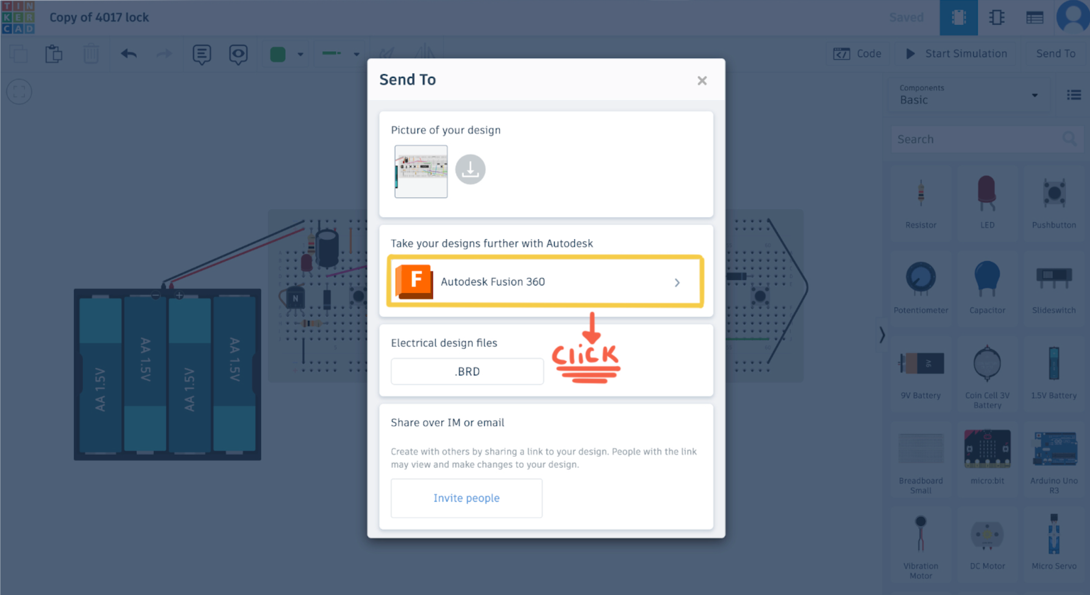
Click send to Fusion 360.
Uploading Your Circuit Onto Fusion 360: 3
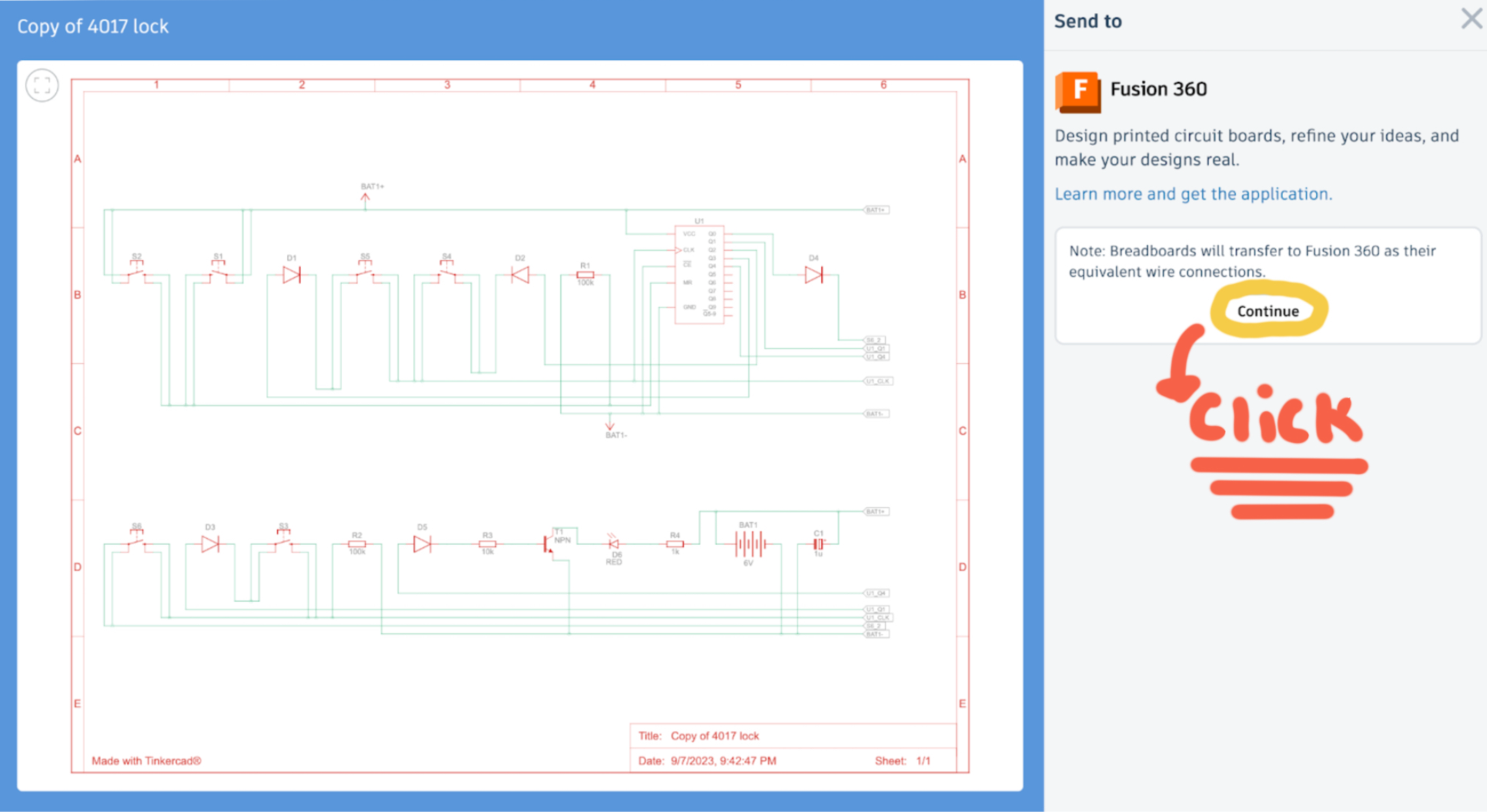
Click continue to complete the send to Fusion 360.
Setting Up Circuit Layout on Fusion: 1
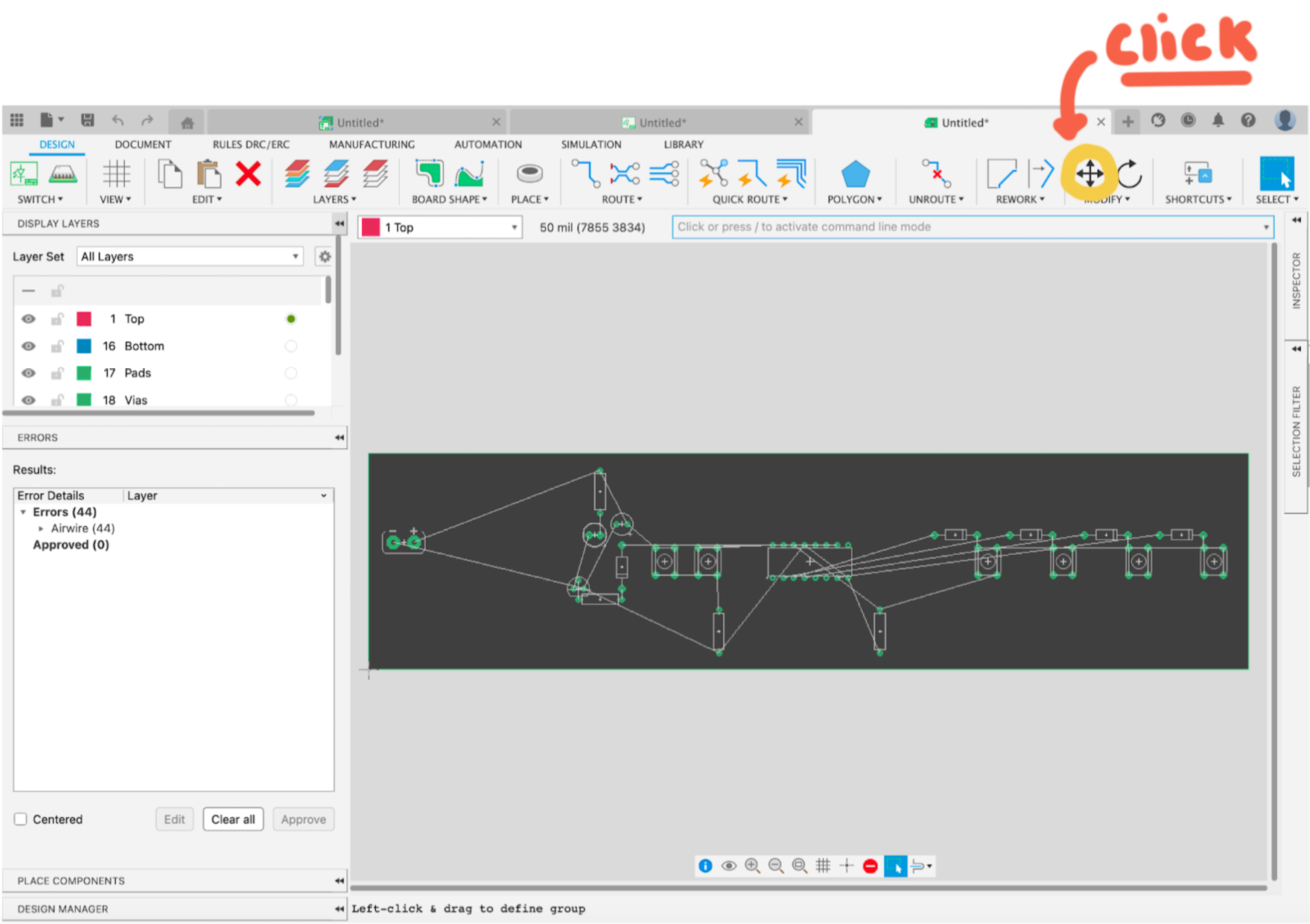
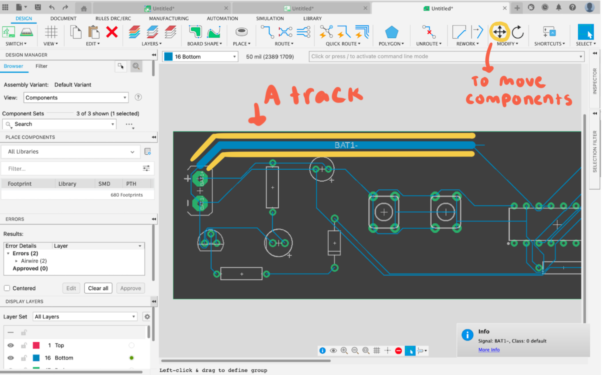
Now that your circuit is on Fusion, you want to begin by arranging all the tracks and components in an organized manner to make for a clean PCB and an easy solder job. Click the cursor-looking shape near the drop-down tab labeled Modify (see in the picture). Now you can rearrange your components to your liking.
Remember that you can place them anywhere you like and nothing will get messed up or change with the functionality of your circuit. Try to have a decent amount of space between the components and tracks.
Setting Up Circuit Layout on Fusion: 2
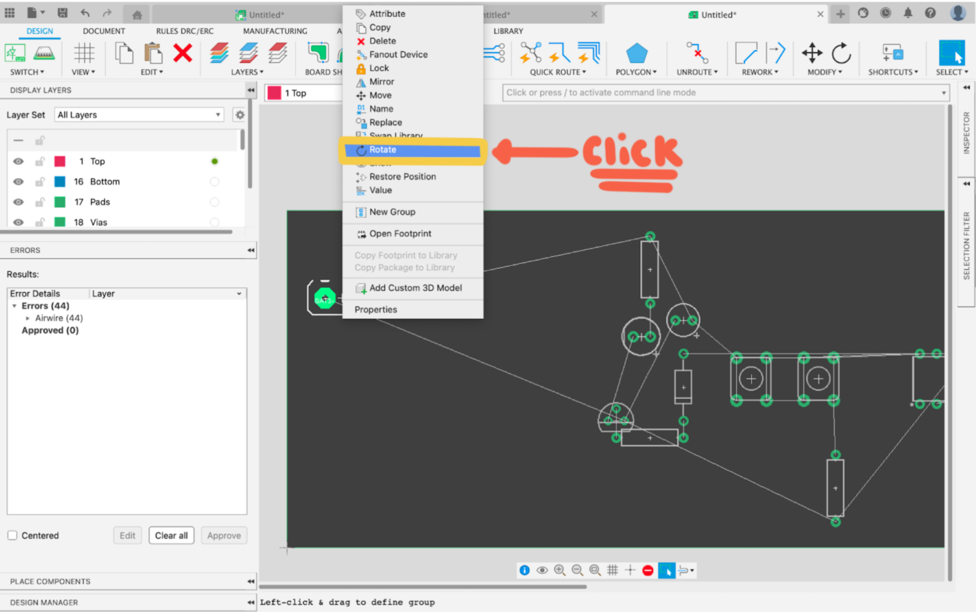
To rotate your components, double-click on any component and click rotate.
Setting Up Circuit Layout on Fusion: 3
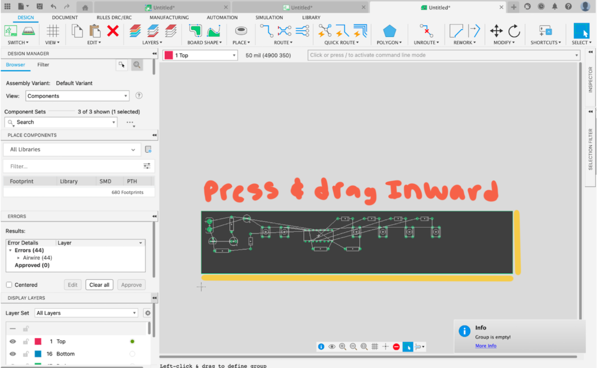
Any access space where there are no components or tracks cut it. Press and hold on the PCB border and drag it inward to trim the access space.
Making the Tracks on Fusion: 1
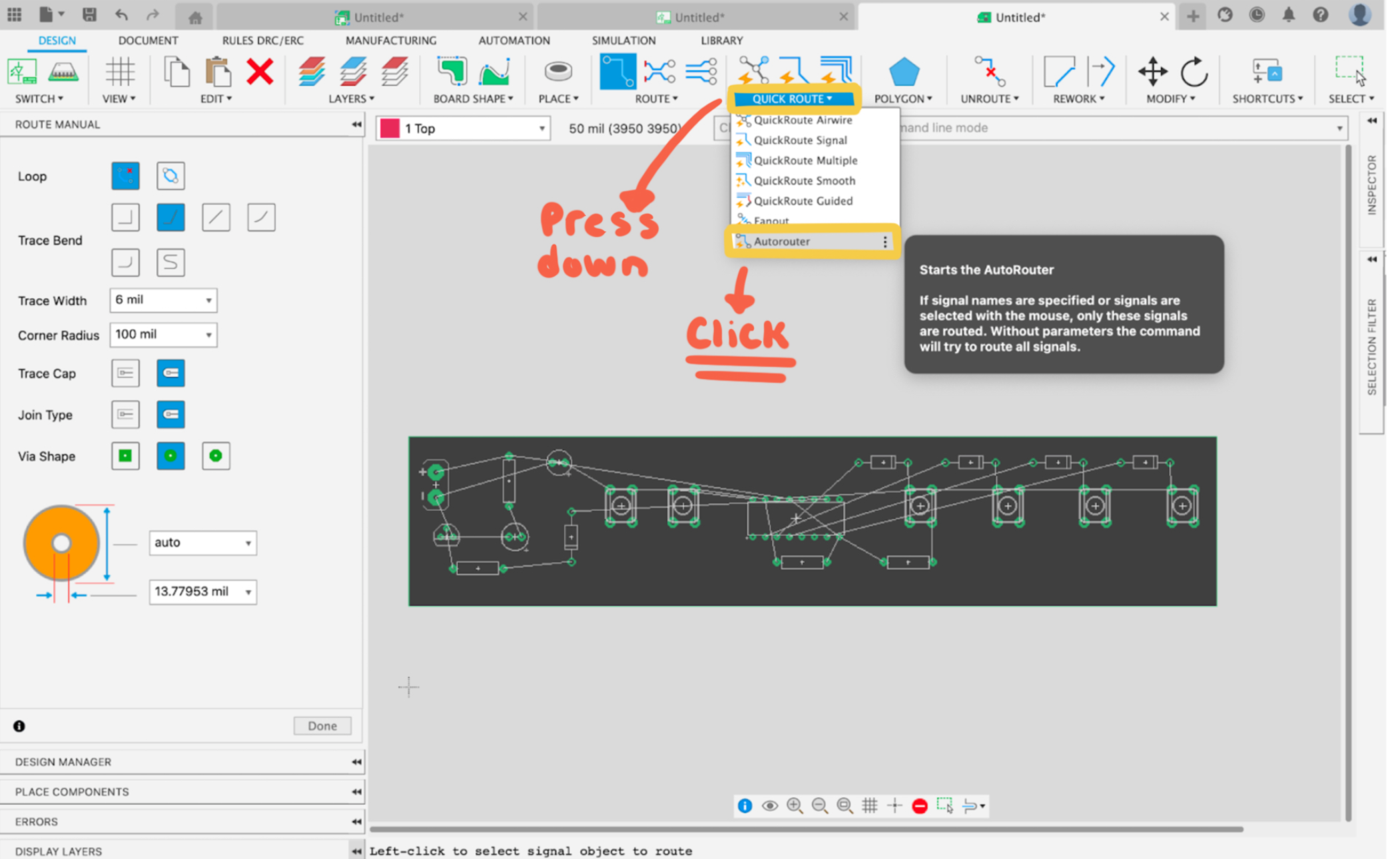
Now we can start making the tracks. Click on the drop-down Quick Route and click on Autorouter. This will give you an outline of where to draw the solder tracks.
Making the Tracks on Fusion: 2
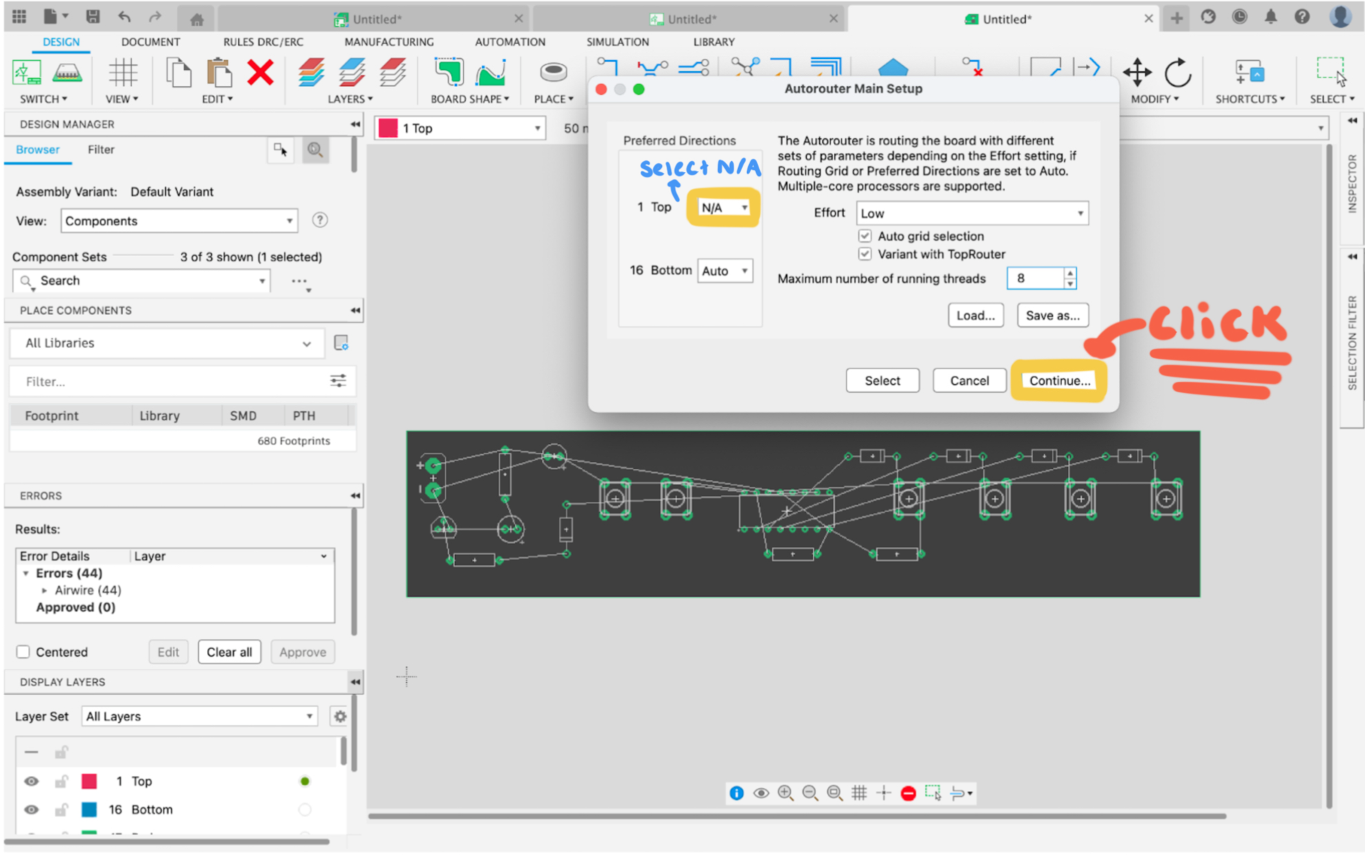
Now you are in the auto-router main setup. Make sure for the label Top that N/A is selected and Bottom auto is selected. Click continue when done.
Making the Tracks on Fusion: 3
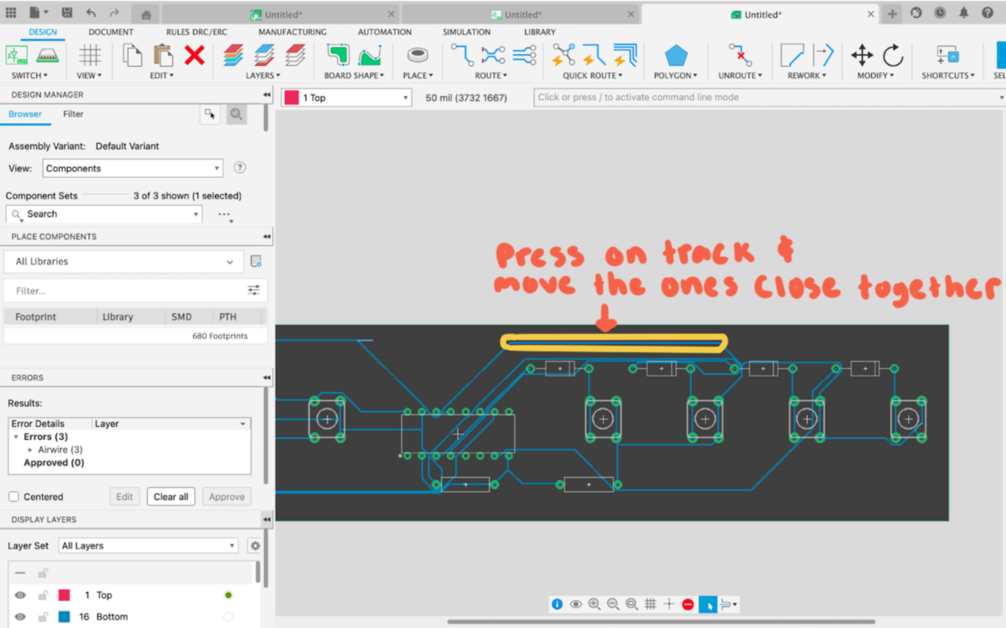
Now you should see thin blue lines on your PCB. Think of these lines as a floor plan or blueprints that will help you place the final tracks correctly. You don't want their tracks to be touching each other or too close as when you draw in the real tracks that are much bigger, there will be connectional errors. Press and hold on to the thin blue tracks and move them to the placement you believe is best suited for your PCB.
Making the Tracks on Fusion: 4
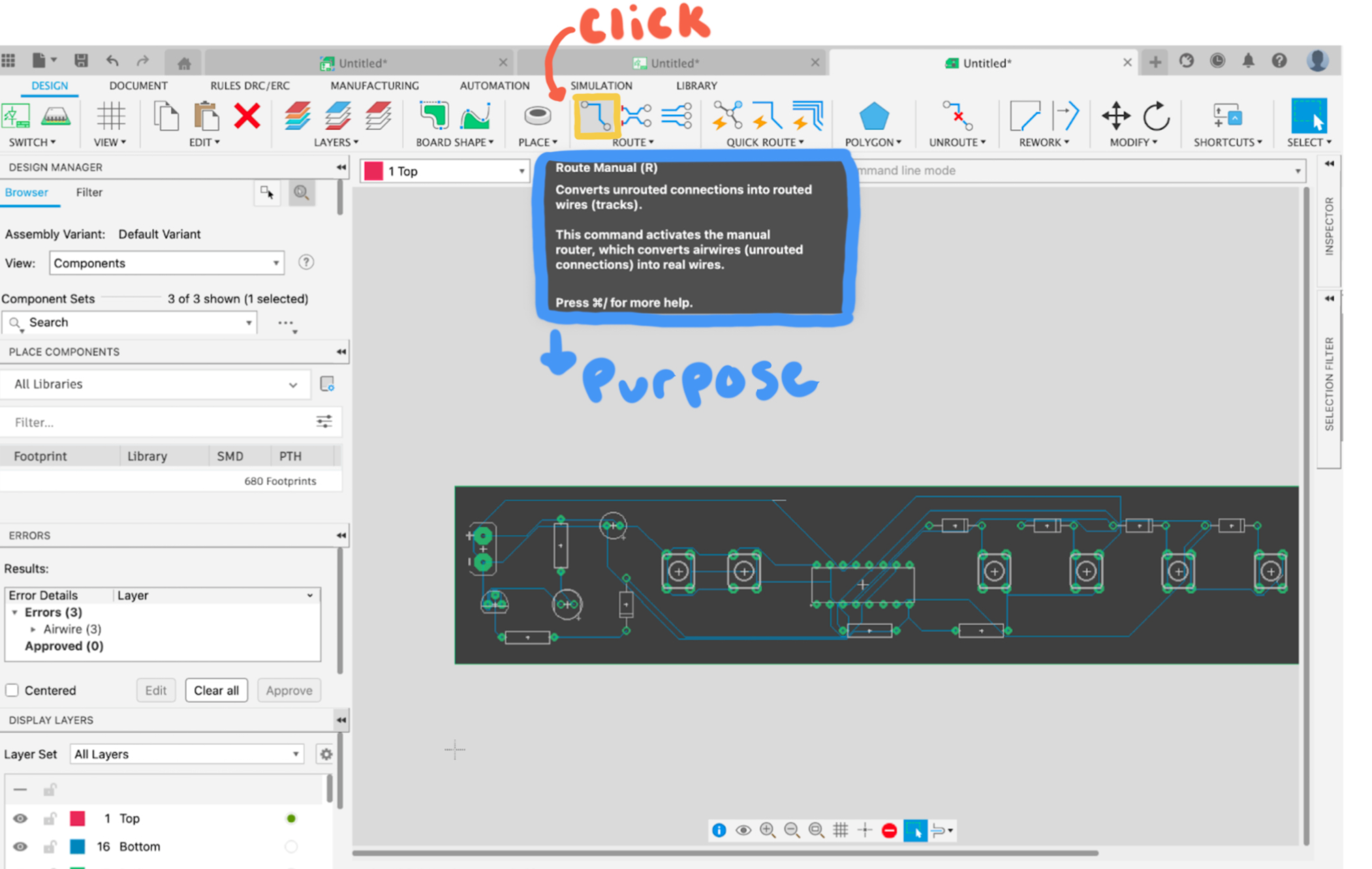
When you are happy with the autoroute tracks, you will now make the finalized tracks. Begin by finding the route drop-down and selecting the route manual button, the symbol furthest to the left. (See the picture)
Making the Tracks on Fusion: 5
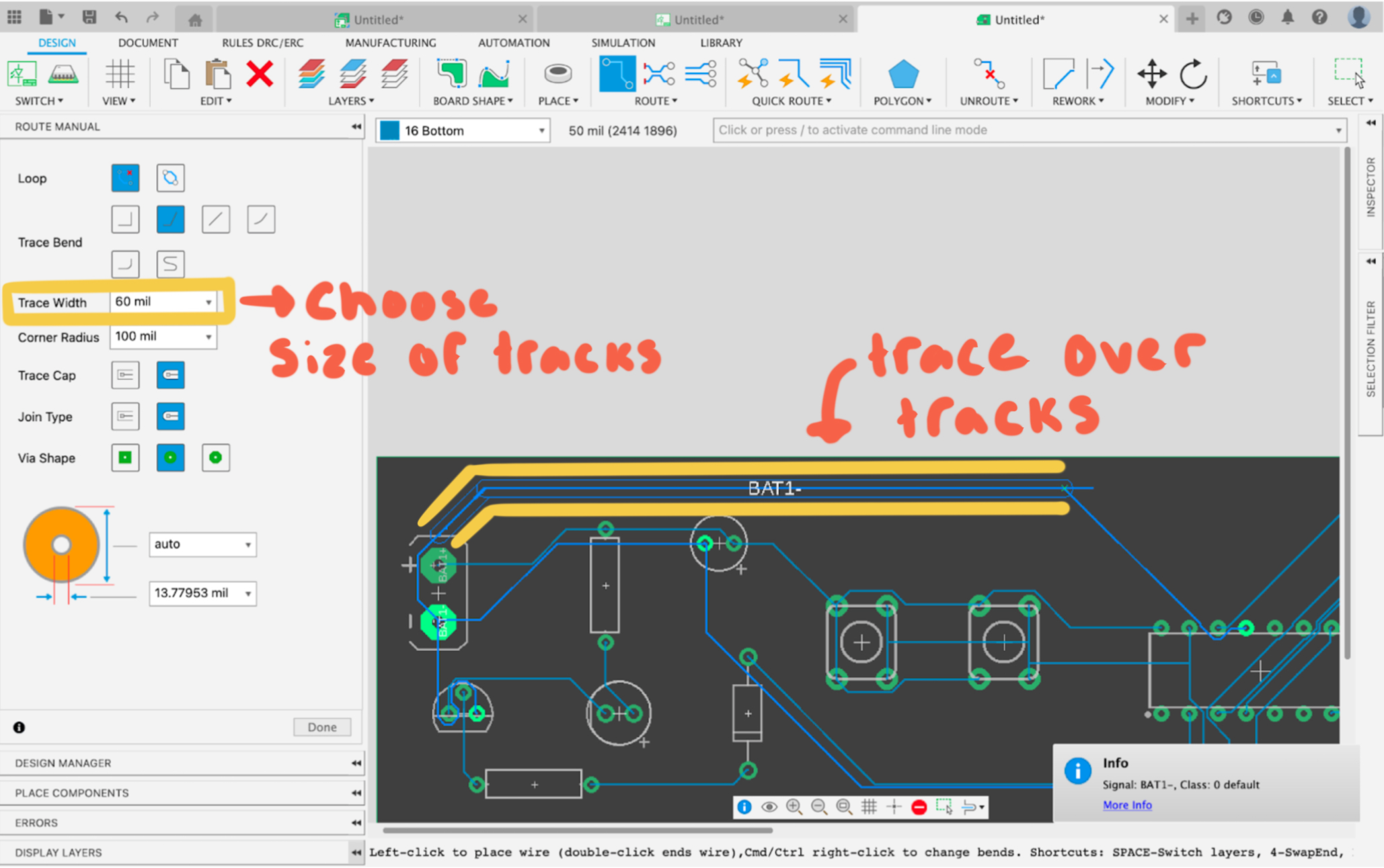
Now you will choose the size of your soldering tracks by changing the value of the trace width. Keep in mind your soldering ability as smaller tracks can be very hard to work with and solder precisely. I recommended using a larger-sized track, I find 60 mils to be a good size. After selecting your track size, trace over your autorouted tracks. You don't have to follow them to perfection, they are just there as a guide. Make sure not to cross any tracks over one another.
Making the Tracks on Fusion: 6
Here is what a track should look like. You can still move the components if the tracks are not fitting and are overlapping one another. (showed in picture)
Sending Off Your PCB :1
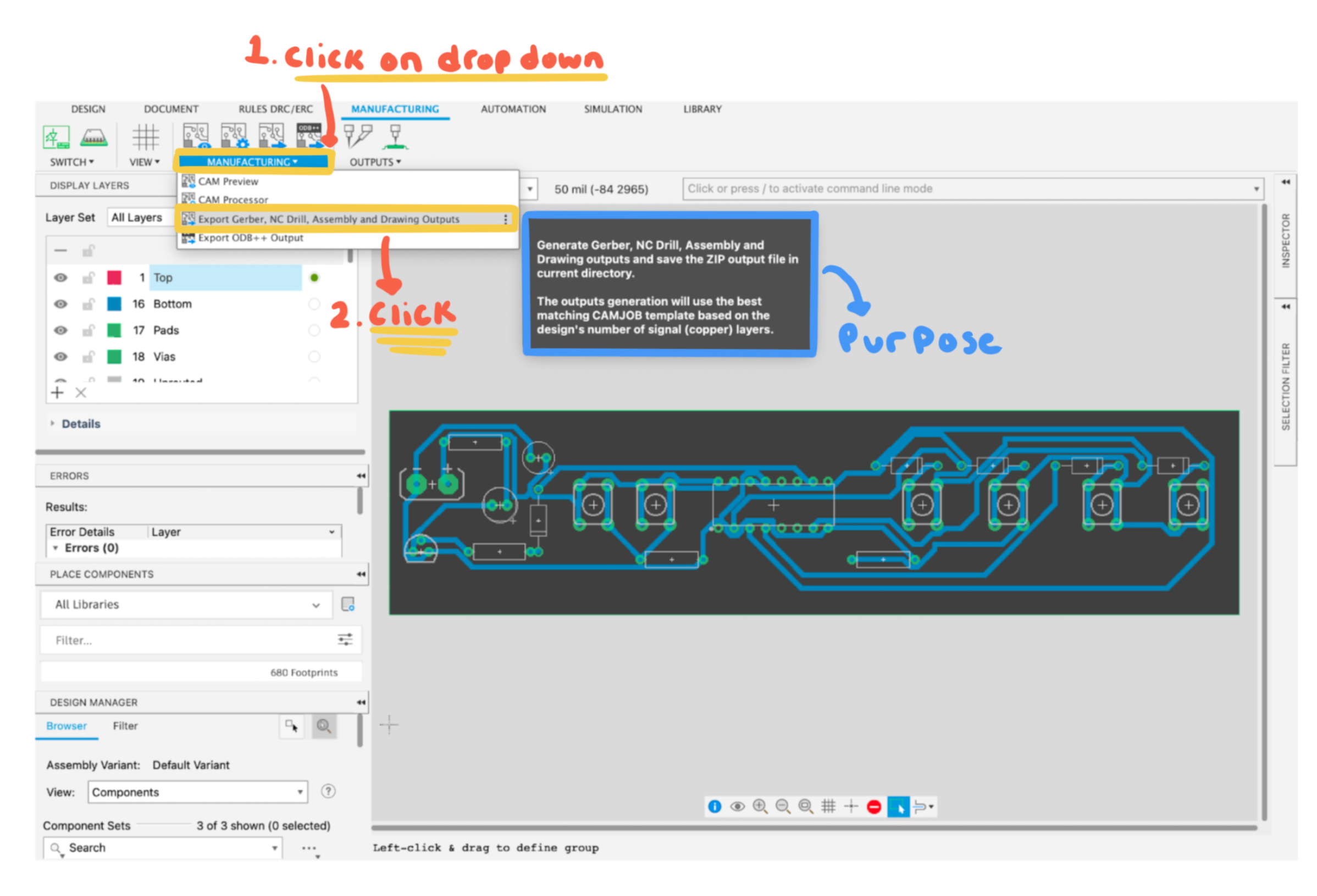
Now that you have completed your tracks, click on the manufacture drop-down button, and click on Export Gerber, NC Drill, Assembly Drawing, and Outputs. This will allow you to create the correct file to send off to JLC to manufacture your PCB.
Sending Off Your PCB : 2
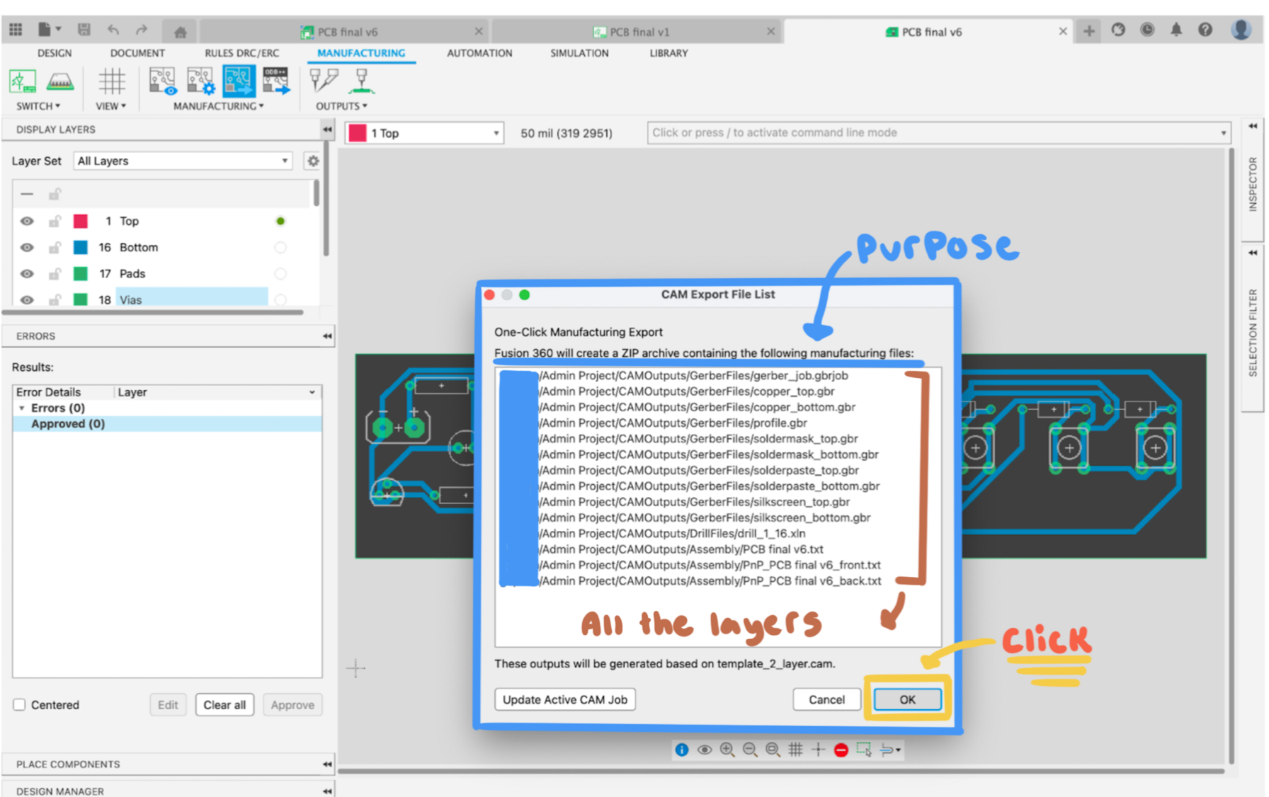
Here are all the layers that make up your PCB. Click continue if you don't see anything missing.
Sending Off Your PCB : 3
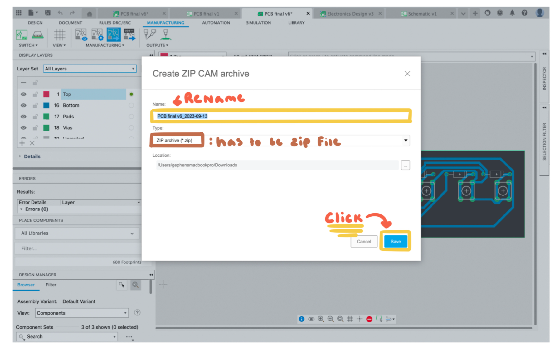
Rename your file to your choosing. Ensure that the file type is a ZIP file. Click save.
Sending Off Your PCB : 4
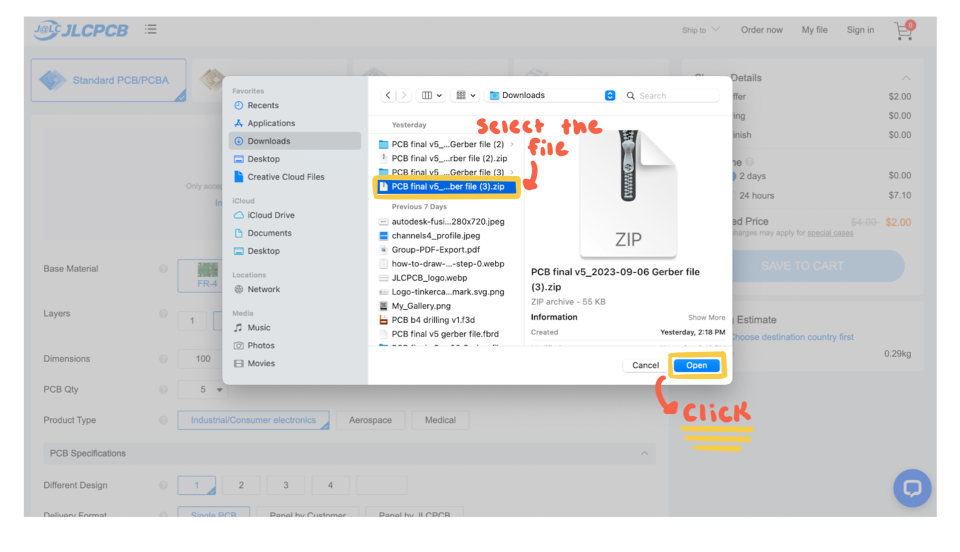
Open JLCPCB and upload the ZIP file you just created. It should be in your downloads.
Sending Off Your PCB : 5
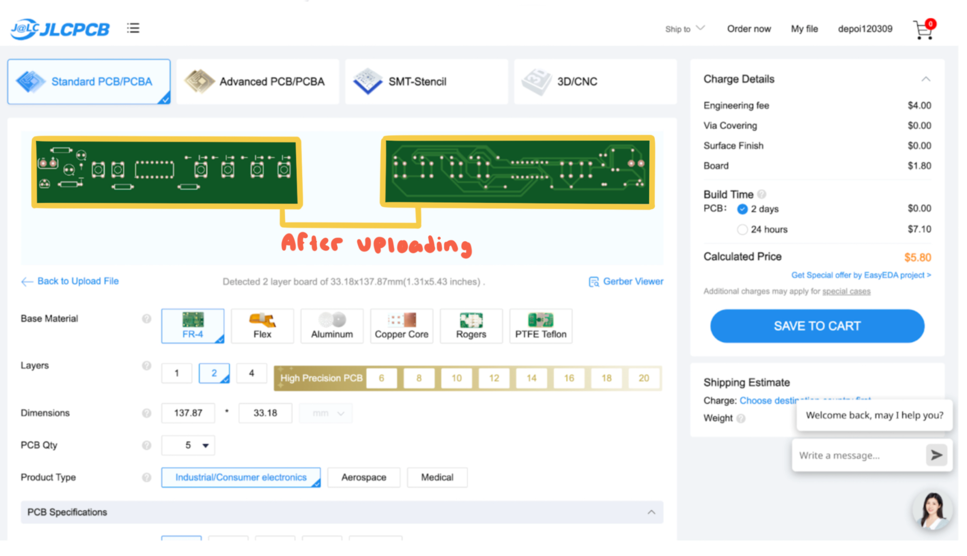
If the file is correctly uploaded you should see the outline of your PCB. (look at picture)
Sending Off Your PCB : 6
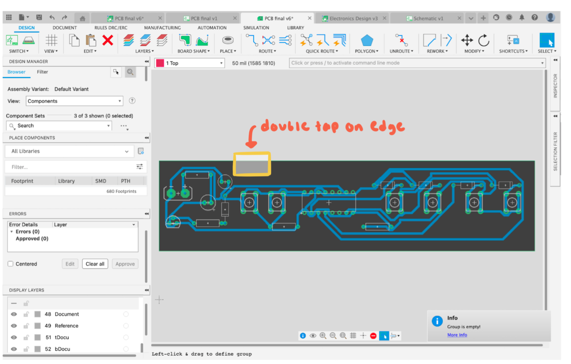
To send off your PCB, you will need the dimensions of your PCB. To find this, double tap on the side edge of the PCB of the dimension you wish to find.
Sending Off Your PCB : 7
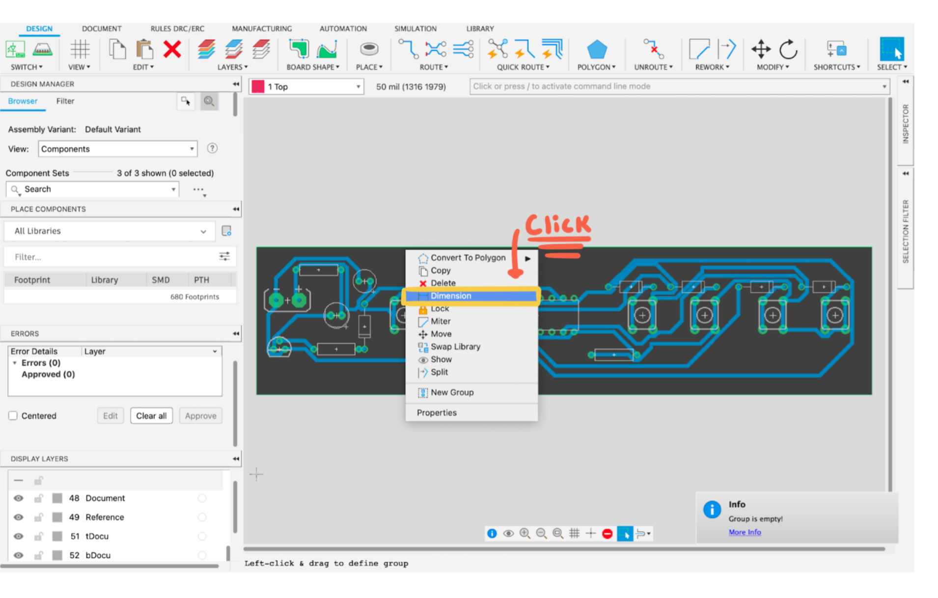
Click dimension.
Sending Off Your PCB : 8
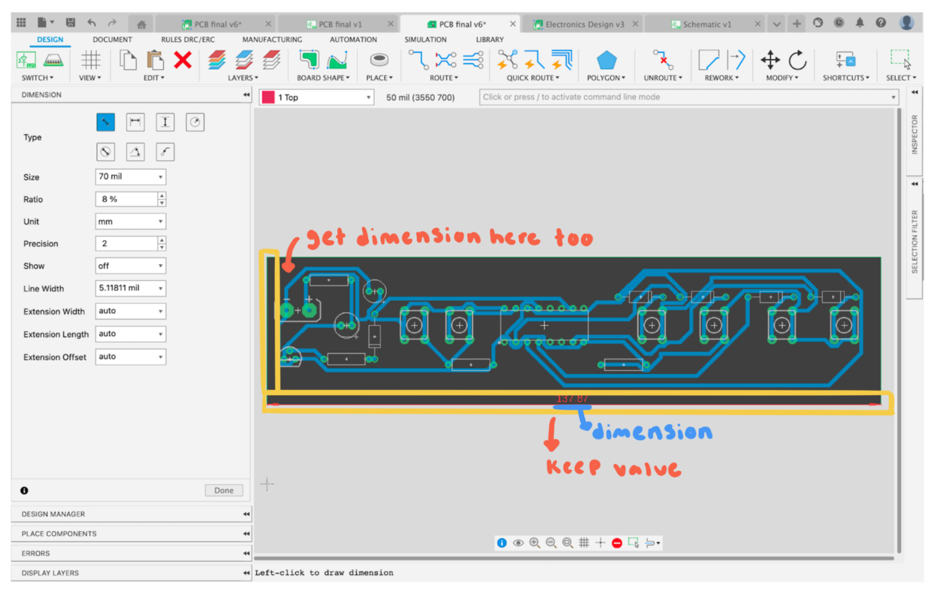
It should tell you the dimensions of the side you selected. Make sure you get the dimensions for both the length and width of your PCB.
Sending Off Your PCB : 9
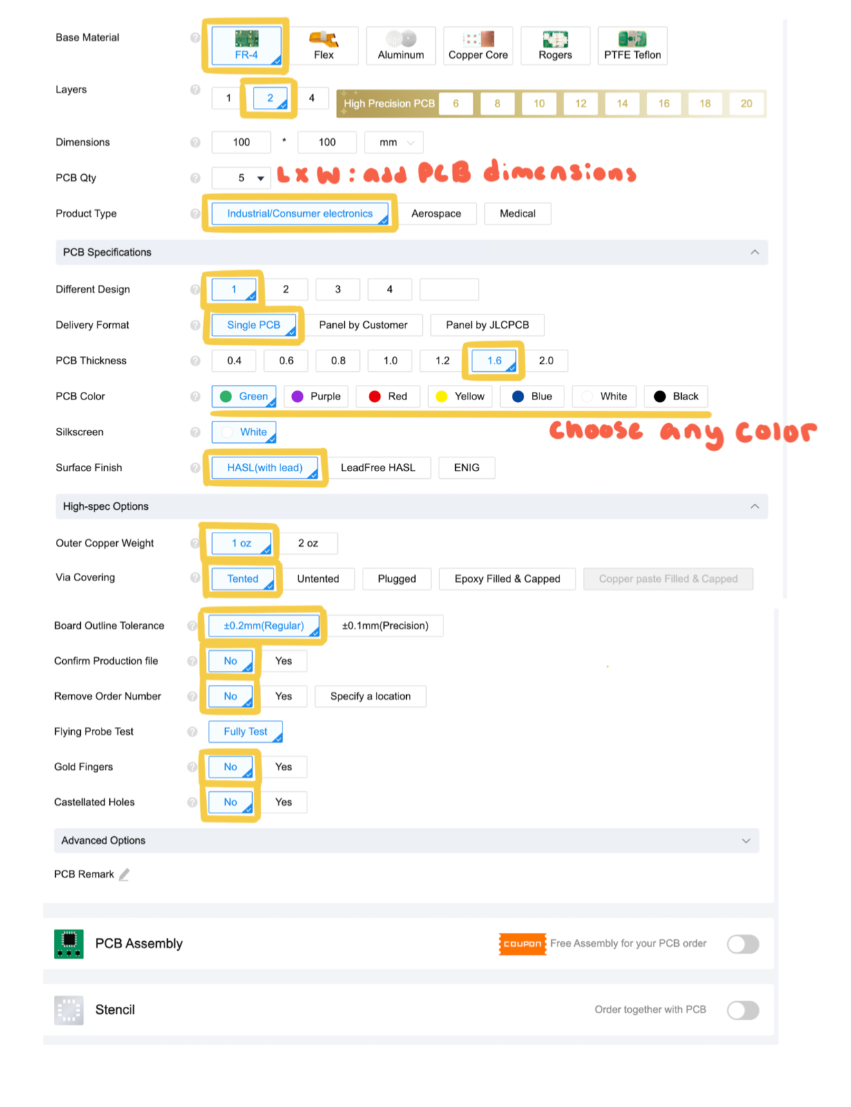
Input the dimensions that you found from steps 18-20. Select the color of the PCB you would like. Make sure all the other settings are the same as highlighted in the picture.
Sending Off Your PCB : 10
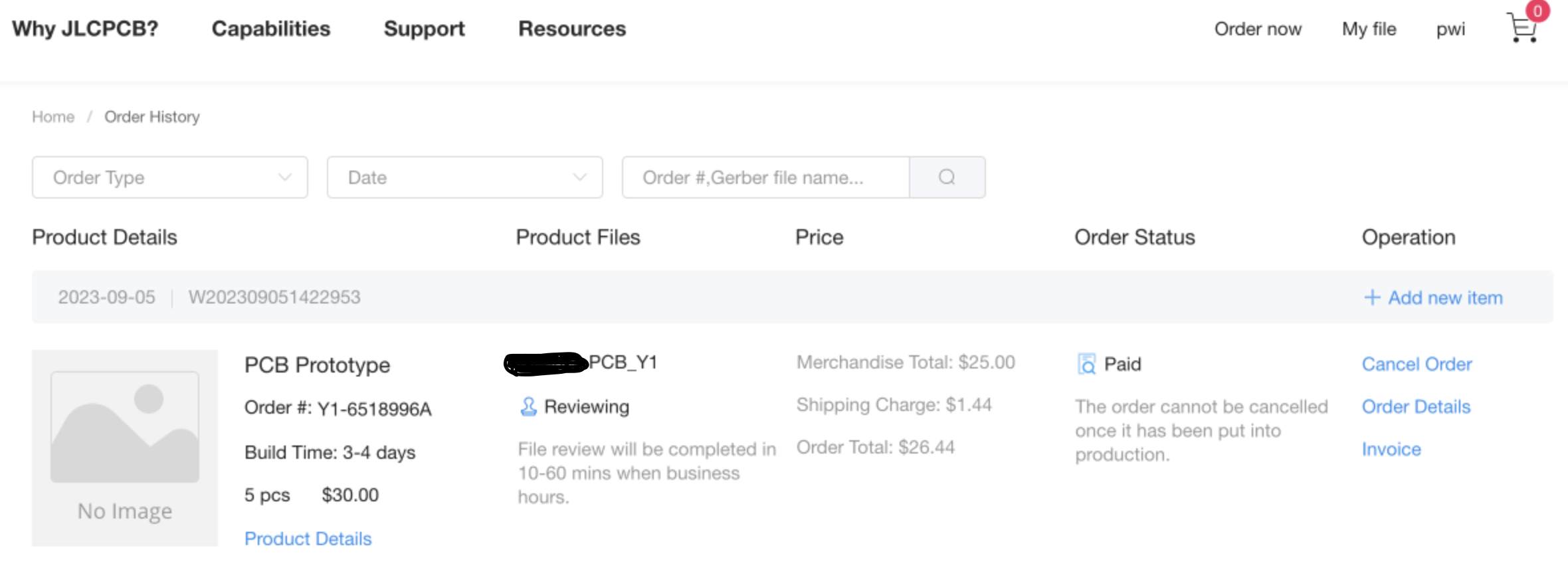
Pay and place your order!
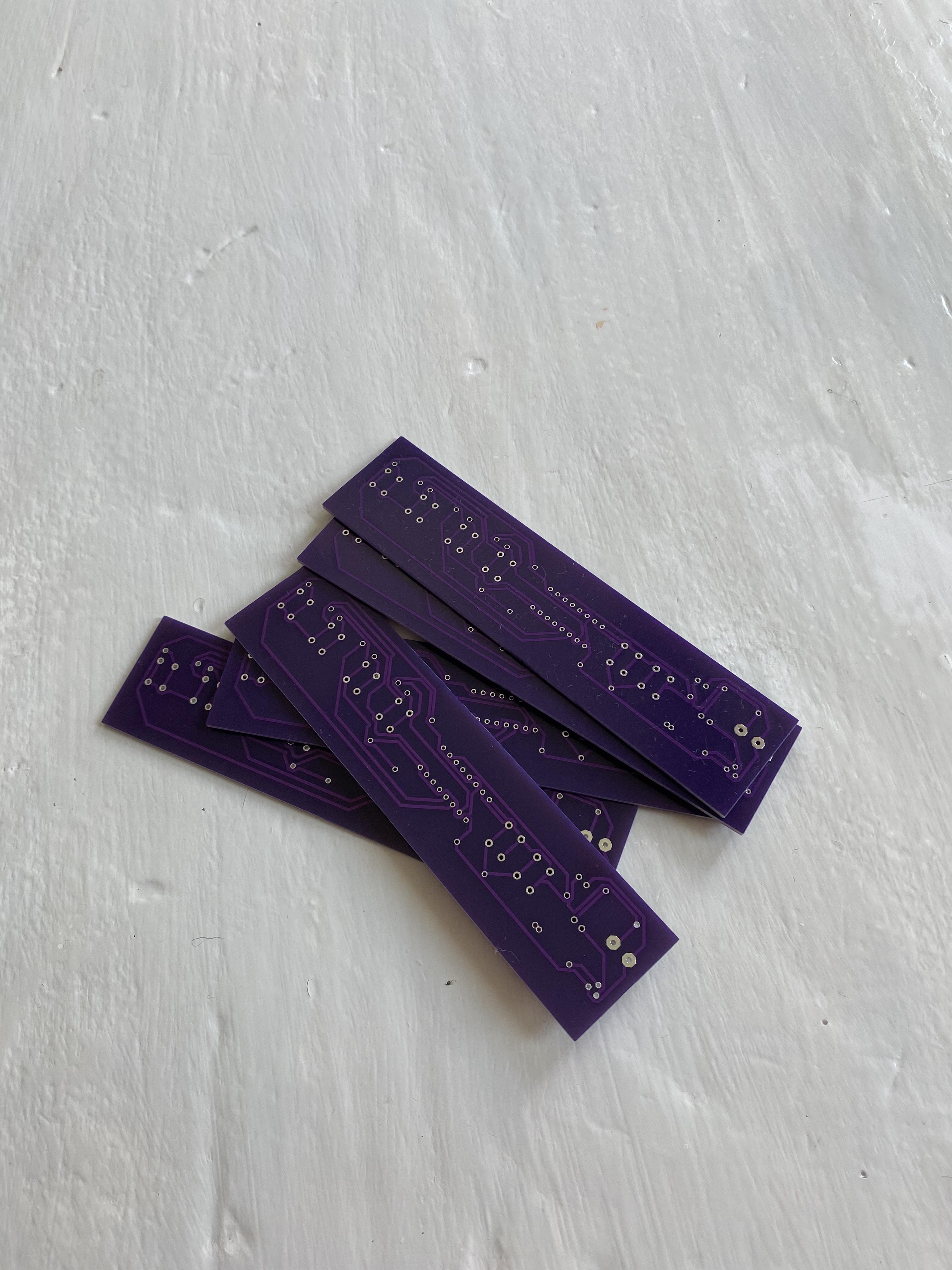
Receiving Your PCB
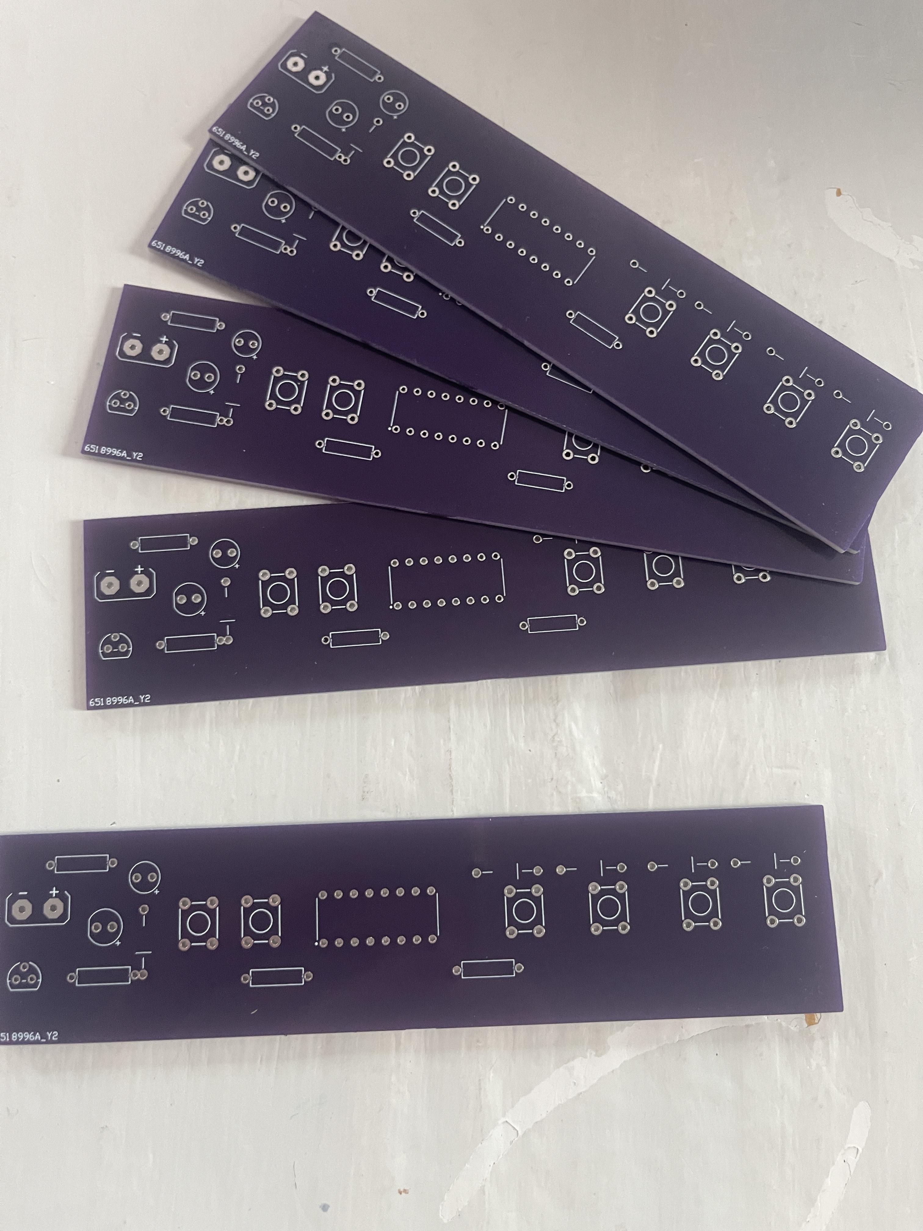
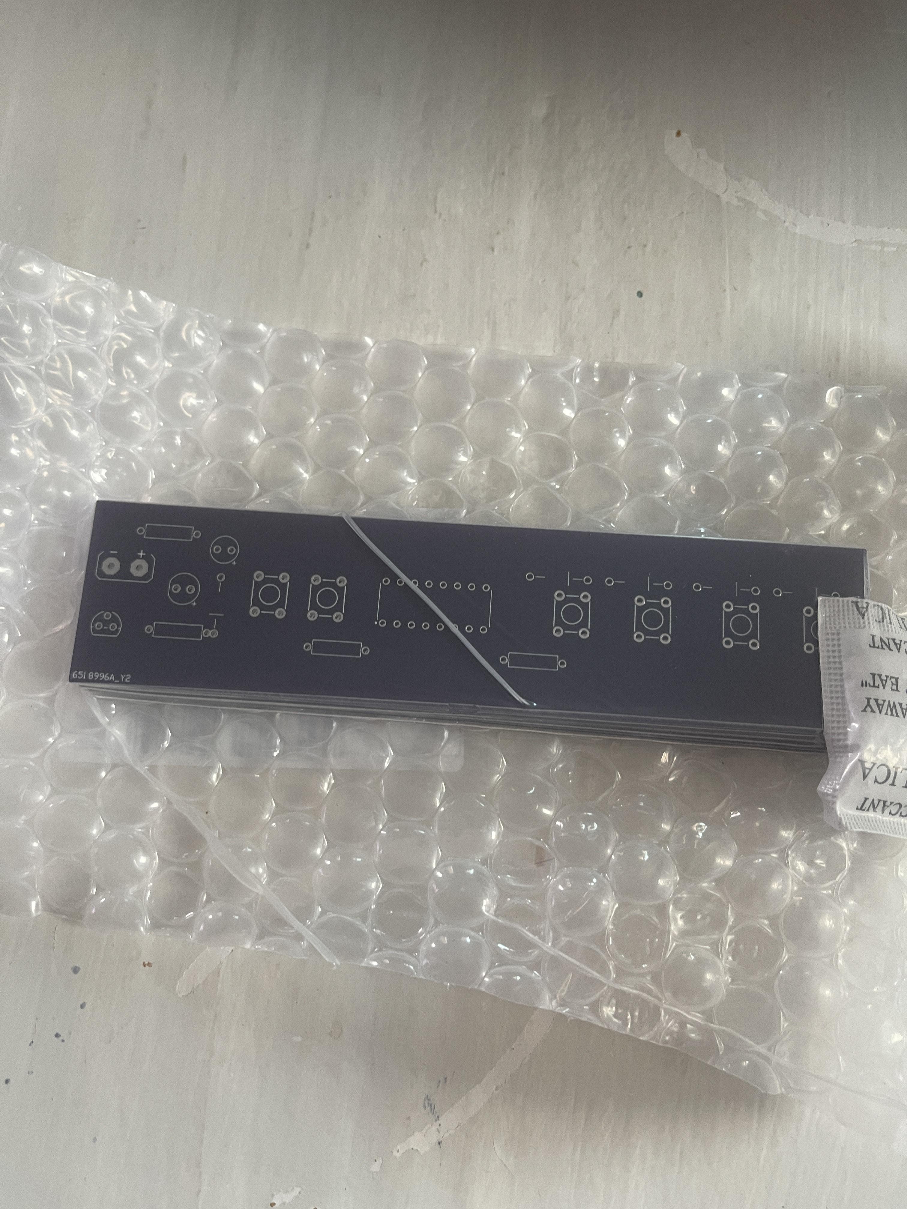

Your order has arrived!
Now you can solder the components to the tracks of the completed functioning PCB.