PCB Hole Size Chart


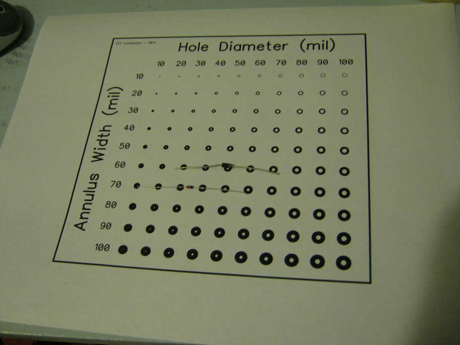
If you're into electronics, you might give PCB layout software a chance. This is what I'm doing because I'm finding that larger projects just take too long to solder by hand with perf-board and wire. This chart is generic so it will work with whichever layout software you chose since the end-file is just an image. The most important thing is to print out the chart without scaling at 600 DPI.
The chart can be found in the zip-file associated with this instructable. The layout software used is DipTrace.
If you want to share your own PCBs for printing, I recommend exporting them as PNGs. To set the resolution for printing, I used ImageMagick's mogrify command as such:
600 DPI is used because this is typically what most laser printers support for toner transfer method and printing.
The chart can be found in the zip-file associated with this instructable. The layout software used is DipTrace.
- Print out the chart without scaling. If you have issues with this in your photo editing programs, try using GIMP.
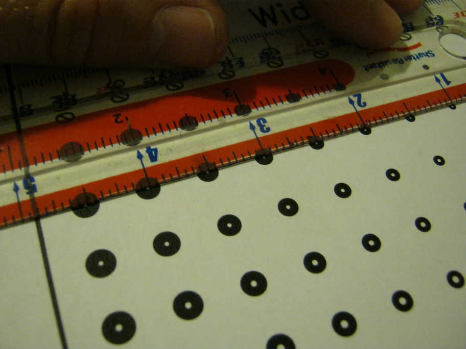
- Measure the hole separation to confirm that it's 1/2 of an inch. If so, it was printed without scaling which is good.
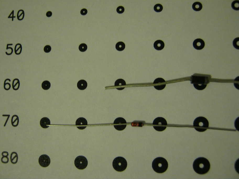
- Place a component lead over a hole, this will give you a rough idea of what to use in your PCB design.
If you want to share your own PCBs for printing, I recommend exporting them as PNGs. To set the resolution for printing, I used ImageMagick's mogrify command as such:
mogrify.exe -units PixelsPerInch -density 600x600 "Hole Chart.png"
600 DPI is used because this is typically what most laser printers support for toner transfer method and printing.