PCB Coils in KiCad

A few weeks back I had made a Mechanical 7 Segment Display that uses electromagnets to push the segments. The project was so well-received, it even got published in Hackspace Magazine! I received so many comments and suggestions that I had to make an improved version of it. So, thank you, everyone!
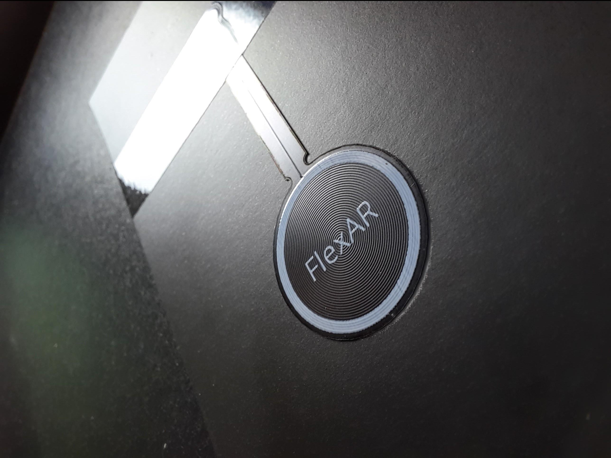
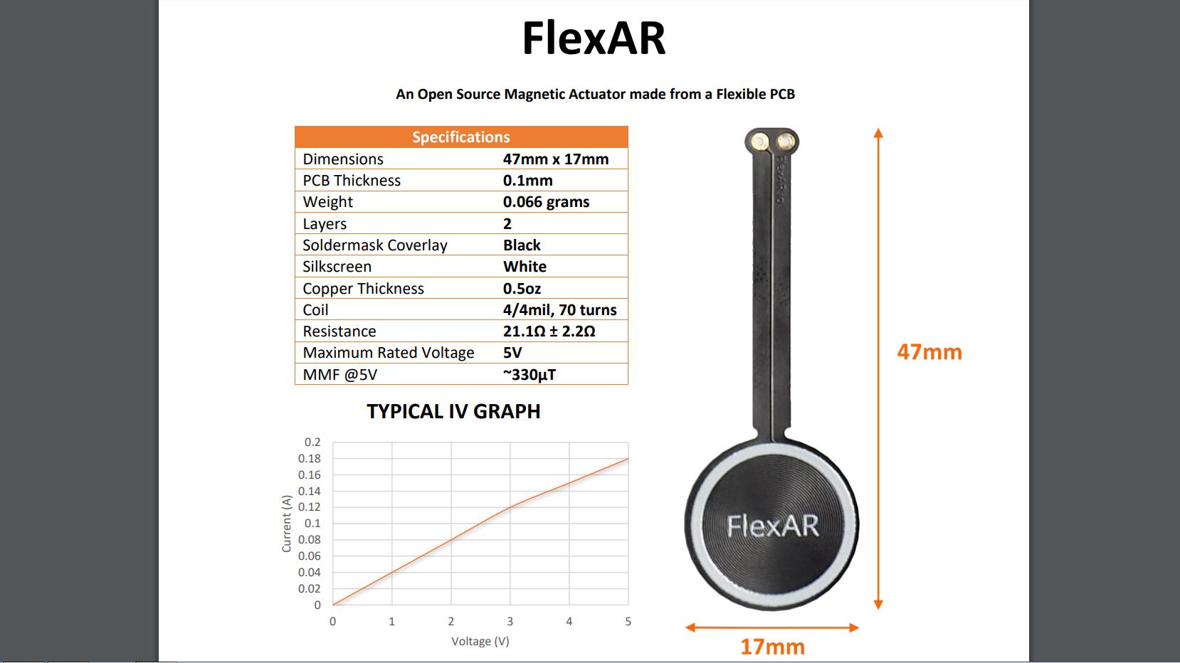
Originally I had planned to make at least 3 or 4 such digits to display some kind of useful information on it. The only thing that stopped me from doing it were the power-hungry electromagnets. Thanks to them, each digit draws about 9A! That’s a lot! Although providing that much current was not a problem but I knew it can be a lot better. But then I came across Carl’s FlexAR project. It is basically an electromagnet on a flexible PCB. He has made some awesome projects using it. Do check out his work! Anyways, it got me thinking if I could use the same PCB coils to push/pull the segments. This means that I could make the display smaller and less power-hungry. So in this Instructable, I will try to make a few variations of the coils and then test them to see which one works the best.
Let’s get started!
The Plan
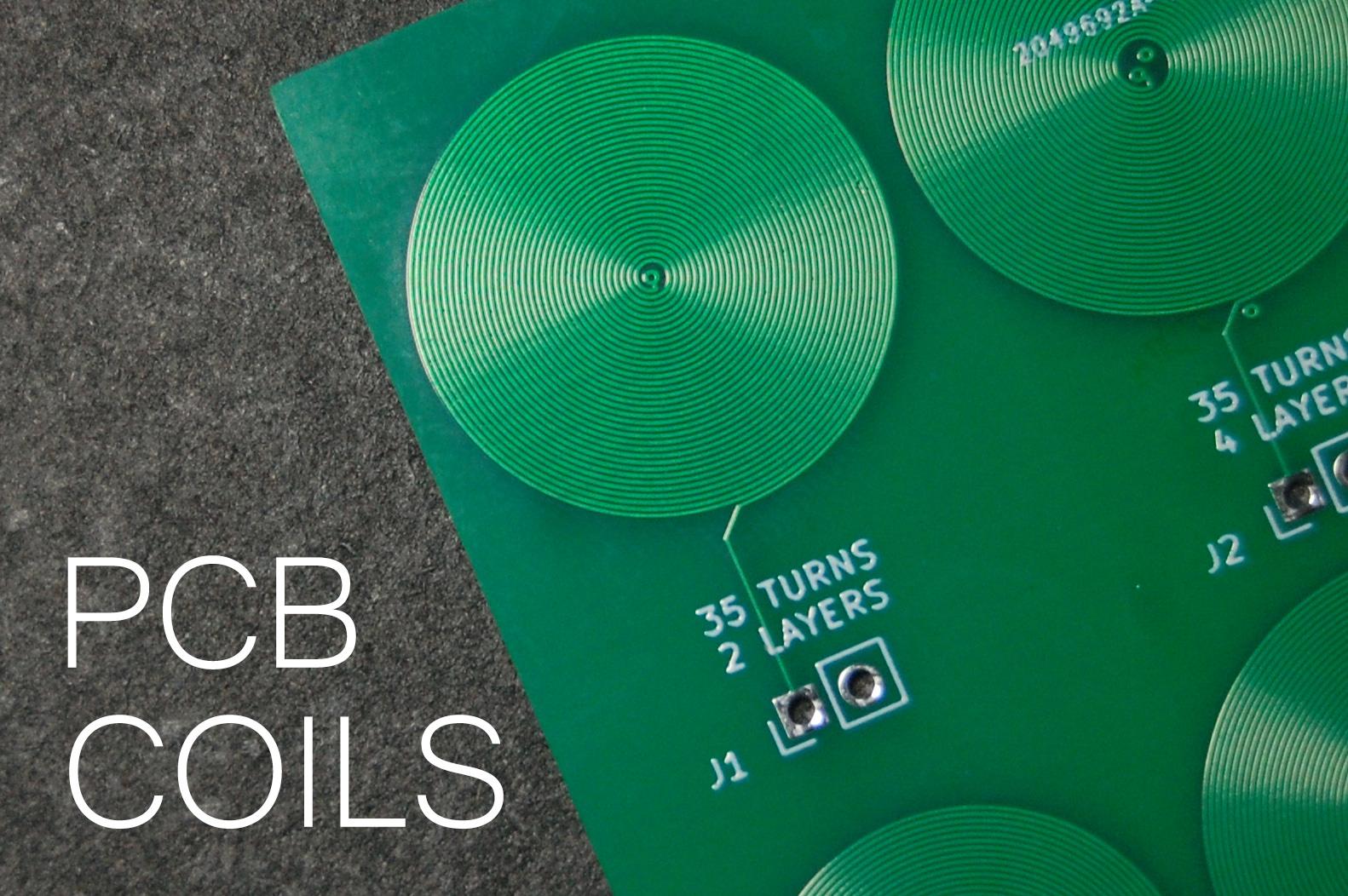
The plan is to design a test PCB with a few variations of coils. It will be a trial and error method.
To start with, I am using Carl's flexible actuator as a reference which is a 2 layer PCB with 35 turns on each layer.
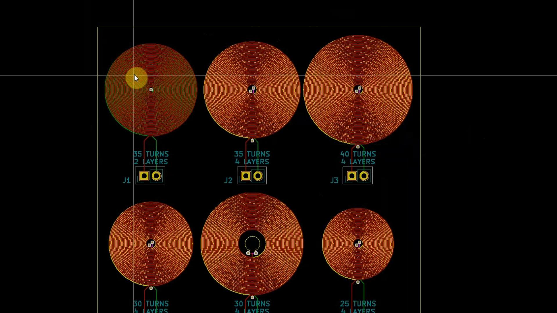
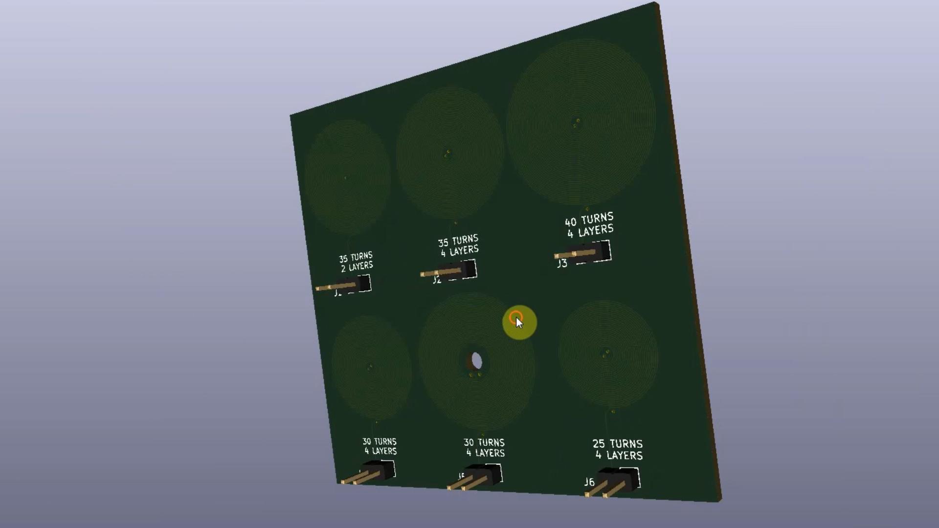
I decided to try the following combinations:
- 35 turns - 2 layers
- 35 turns - 4 layers
- 40 turns - 4 layers
- 30 turns - 4 layers
- 30 turns - 4 layers (with a hole for the core)
- 25 turns - 4 layers
Now here comes the difficult part. If you have used KiCad, you may know that KiCad does not allow curved copper traces, only straight traces! But what if we join small straight segments in such a way that it creates a curve? Great. Now continue doing this for a few days till you have one complete coil!!!
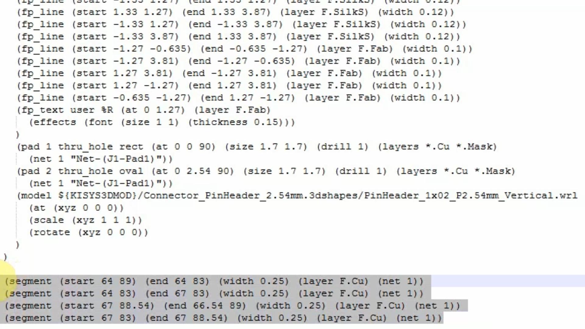
But wait, if you look at the PCB file, which KiCad generates, in a text editor, you can see that each and every segment’s position is stored in the form of x and y coordinates along with some other information. Any changes here will be reflected in the design as well. Now, what if we could enter all the positions needed to form a complete coil? Thanks to Joan Spark, he has written a Python script which after entering a few parameters spits out all the coordinates needed to form a coil.
Carl, in one of his videos, has used Altium's Circuit Maker to create his PCB coil, but I didn't feel like learning new software. Maybe later.
Making Coils in KiCad
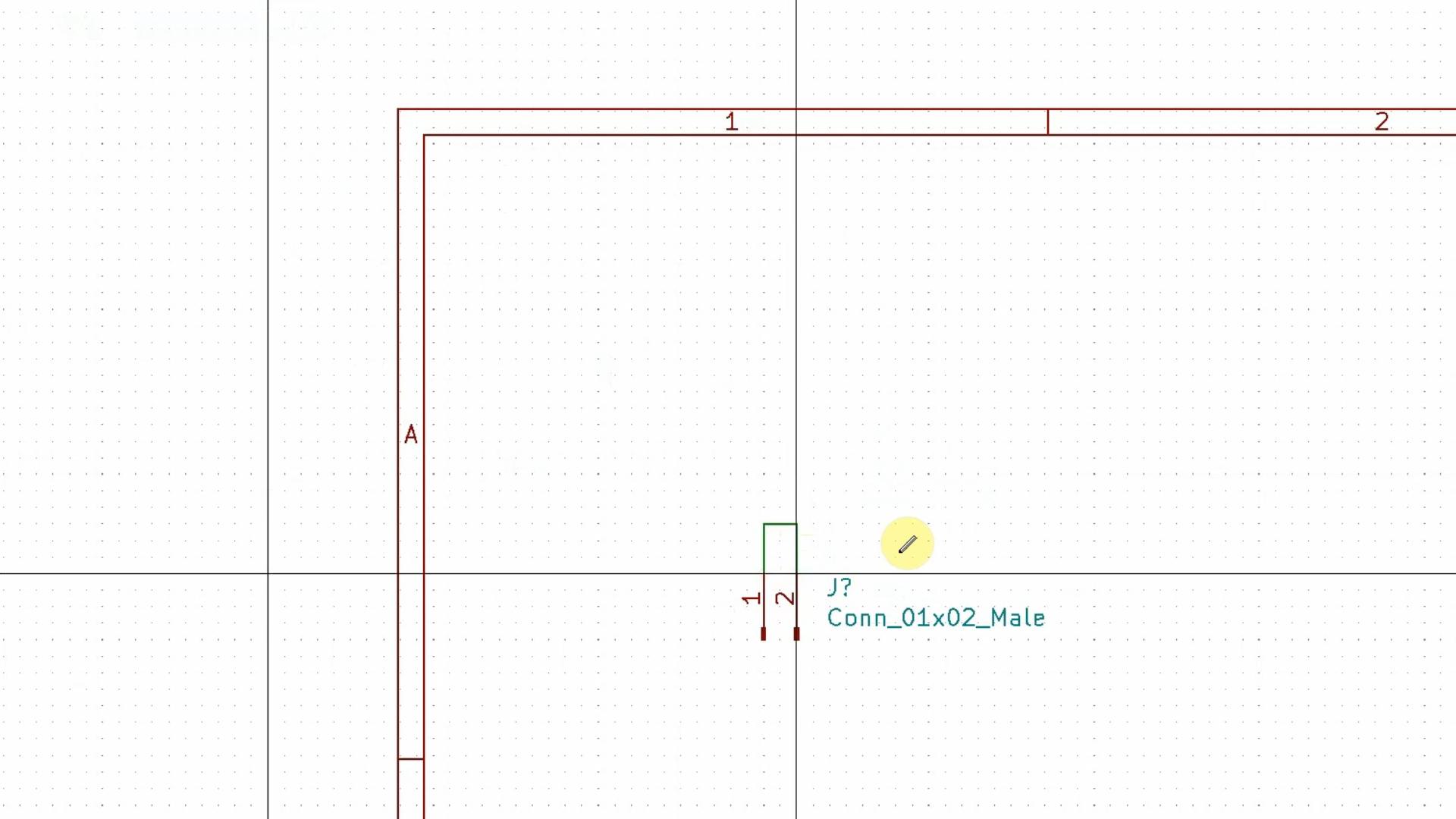
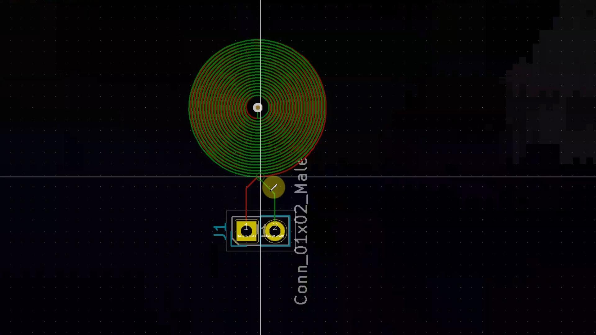
First I placed a connector on the schematic and wired it as shown above. This wire will become a coil in the PCB layout.
Next, you need to remember the net number. The first one will be net 0, the next will be net 1, and so on.
Next, open the python script using any suitable IDE.
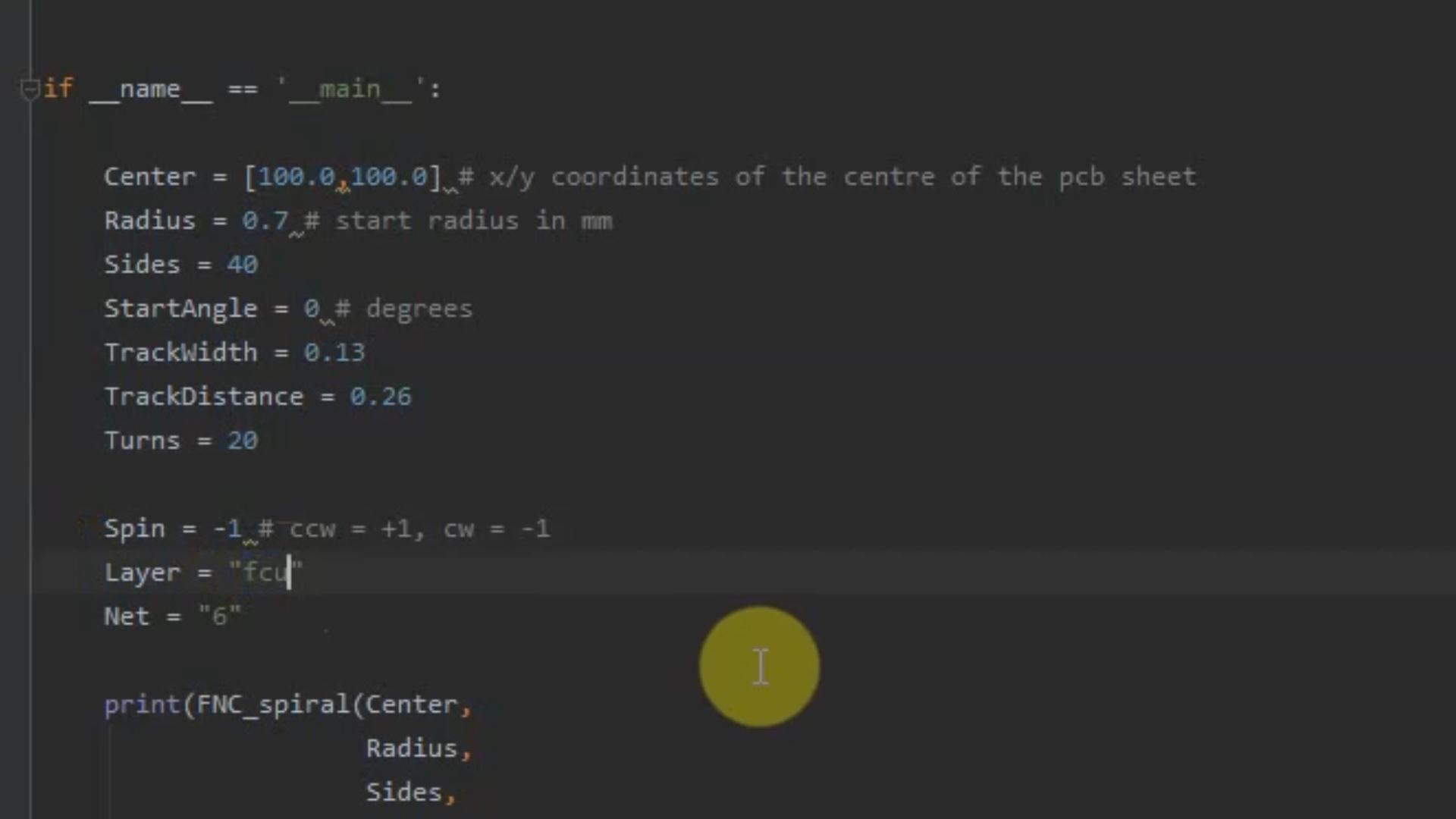
Choose the trace width you will be using. After that, try experimenting with sides, start radius and track distance. Track distance should be double the track width. The greater the number of 'sides', the smoother will be the coil. Sides = 40 works best for most of the coils. These parameters will remain the same for all coils.
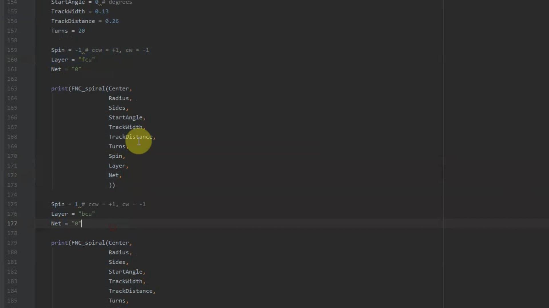
You need to set a few parameters like center, number of turns, copper layer, net number and most importantly, the direction of rotation (spin). While going from one layer to another, the direction must change in order to keep the direction of the current same. Here, spin = -1 represents clockwise while spin = 1 represents counterclockwise. For example, if the front copper layer is going clockwise then the bottom copper layer must go counterclockwise.
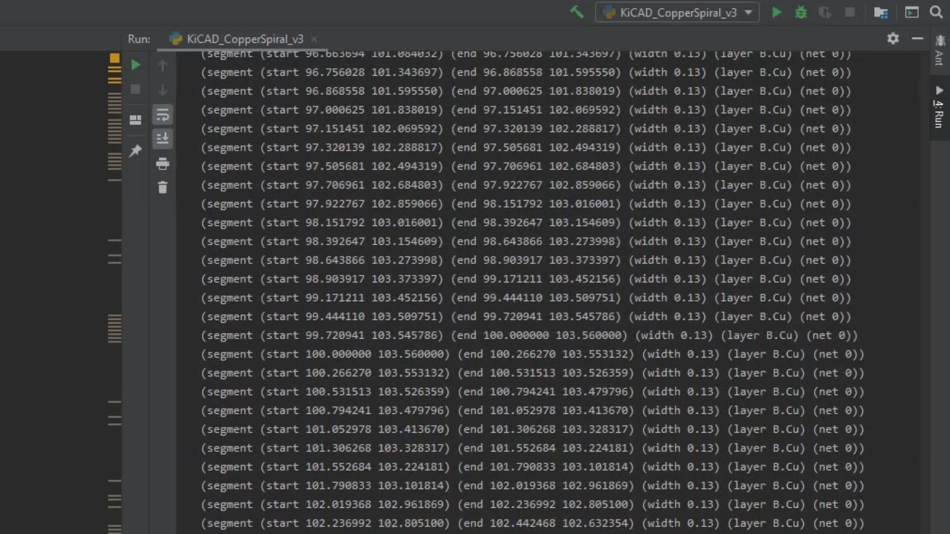
Run the script and you will be presented with a lot of numbers in the output window. Copy and paste everything into the PCB file and save it.
Open the PCB file in KiCad and there’s your beautiful coil.
Finally, make the remaining connections to the connector and you’re done!
Ordering PCBs
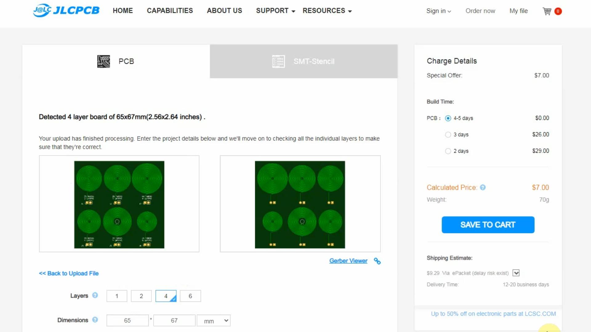
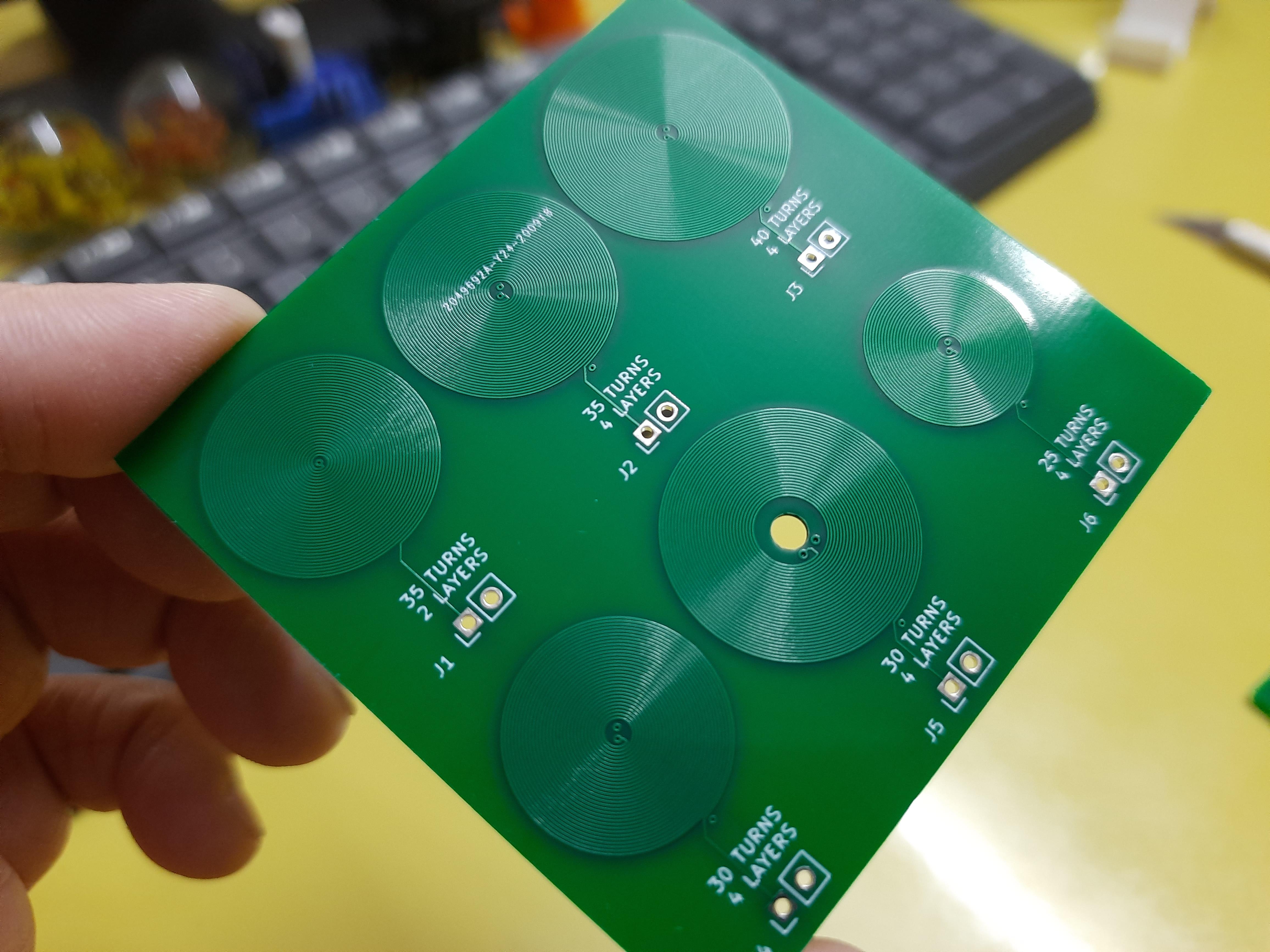
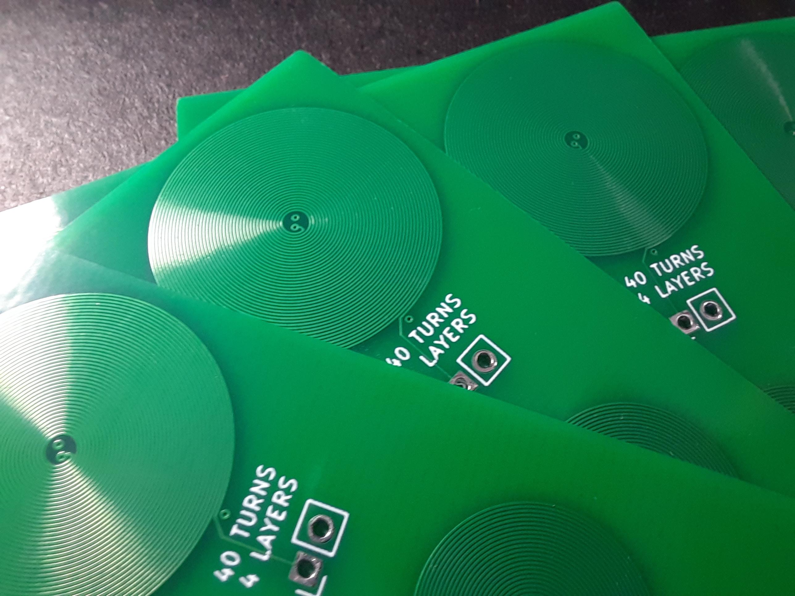
While designing coils, I have used 0.13mm thick copper trace for all the coils. Though JLCPCB can do a minimum trace width of 0.09mm for 4/6 layers PCB, I didn't feel pushing it too close to the limit.
After I was done designing the PCB, I uploaded the gerber files to JLCPCB and ordered the PCBs.
Click here to download the gerber files if you wish to try it out.
Making Test Segments
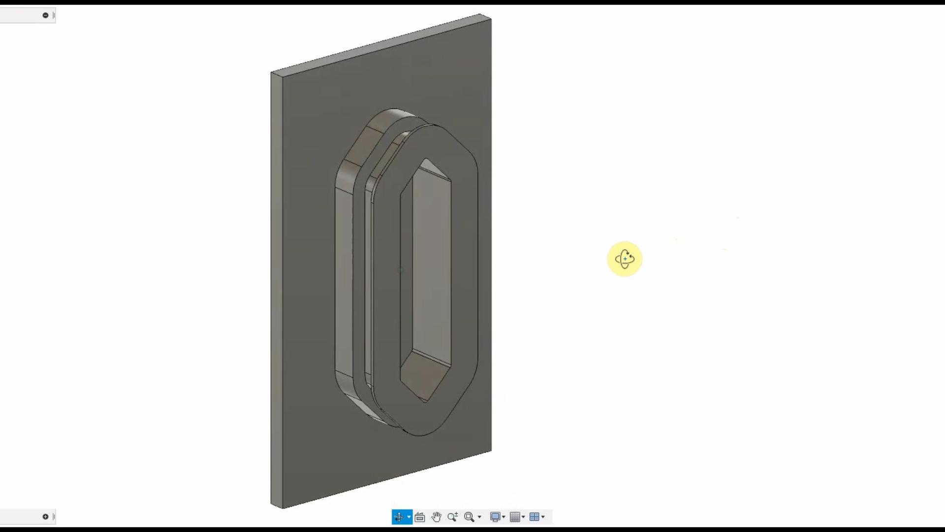
I designed a few test segments of different shapes and sizes in Fusion 360 and 3D printed them.
Since I have used 0.13 mm copper trace for the coils, it can handle a maximum current of 0.3A. The electromagnet which I had used in the first build draws up to 1.4A. Clearly, there will be a considerable reduction in the force which means that I have to make the segments light in weight.
I scaled down the segment and reduced the wall thickness, keeping the shape the same as before.
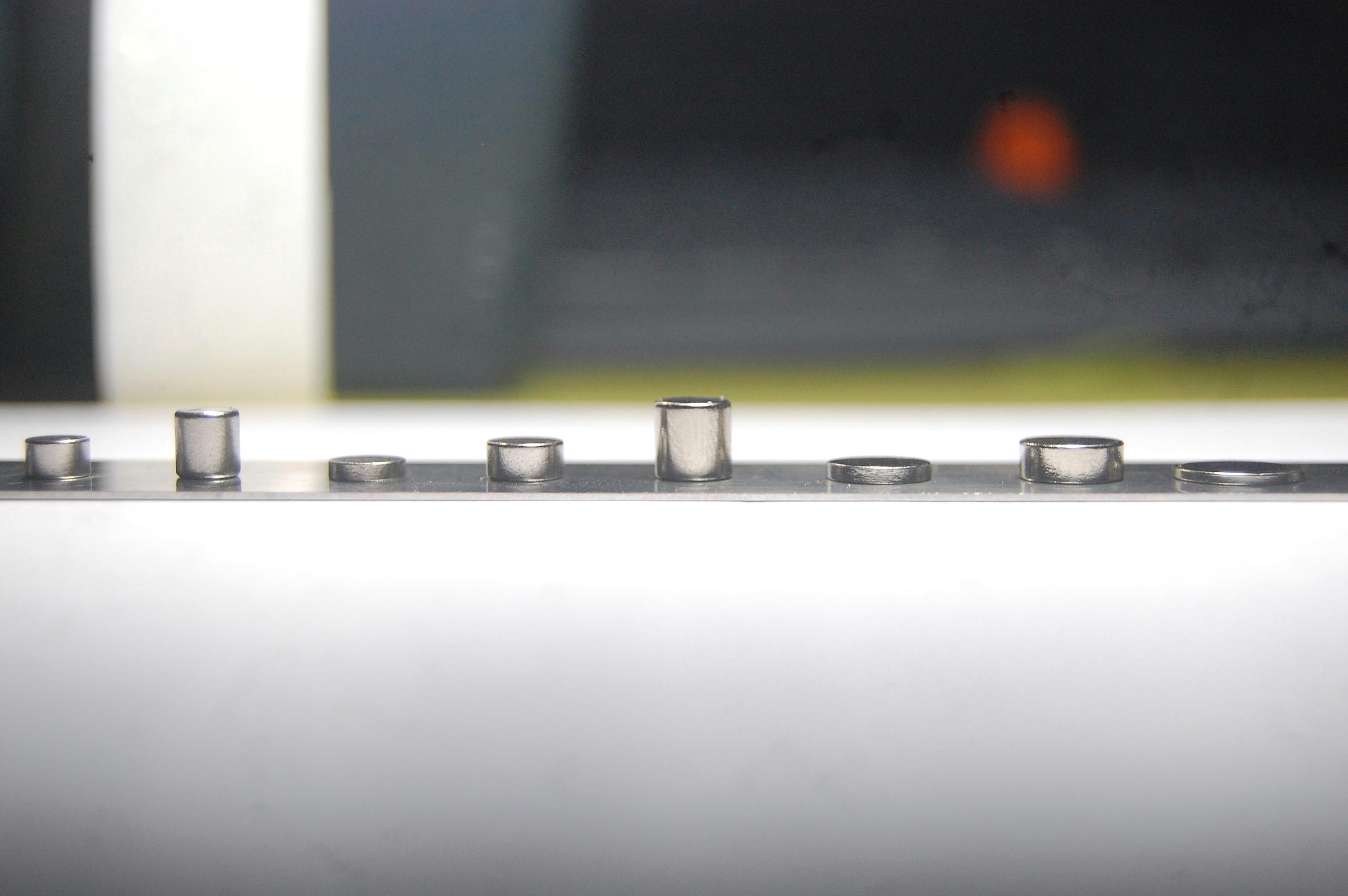
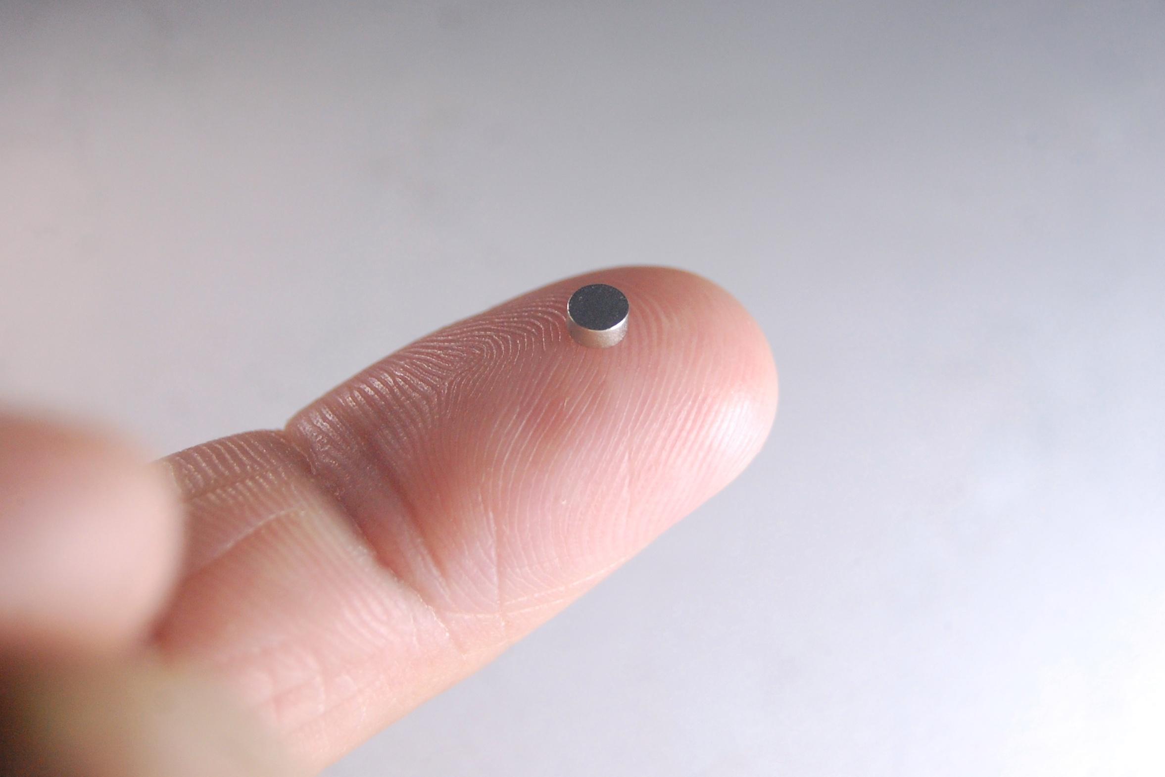
I even tested it with different magnet sizes.
Conclusion
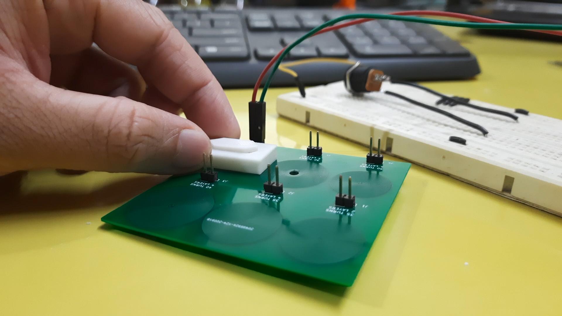
I found out that a coil with 4 layers and 30 turns on each layer along with a 6 x 1.5mm neodymium magnet was sufficient to lift the segments. I am very happy to see the idea working.
So that's it for now. Next, I will be figuring out the electronics for controlling the segments. Let me know your thoughts and suggestions in the comments below.
Thank you for sticking to the end. I hope you all love this project and learned something new today. Subscribe to my YouTube channel for more such projects.