OverEngineered Pen Holder


Hello and welcome back, everyone. Today's crazy and exciting project is THE OVERENGINEERED Pen Holder, which is constructed mostly from PCBs and some 3D-printed components.
The concept of this story was that after using a mug as a pen holder for some years, it was time for an upgrade—an OverEngineered upgrade.
I utilized four square PCBs and a few 3D-printed components to create a new pen holder. Three PCBs are only there for aesthetic purposes, but the one on the backside of the device has a power management IC that is being used to operate any 5V device, such as an Arduino board, or even charge a smartphone.
It also has a few RED LEDs that light up the entire system and make it appear like a lamp in the dark.
A 3D-printed pen holder would be easy to make, but where's the fun in that? This pen holder's overengineered design and built-in battery boost its usability and visual appeal, which in my opinion, makes it far superior to a pen holder that is entirely 3D printed.
This Instructables is about how this project was built, so let's get started.
Supplies
These were the materials used in this built-
- IP5303 IC
- Custom PCBs
- 10uF Capacitor 0805 package
- 2 Ohms resistance 1206 package
- USB Micro Port
- USB Port
- Tactile Switch
- ON OFF Switch
- RED LEDs 5mm (you can use any color)
- 3D Printed part
OverEngineered Pen Holder 3D Model


The foundation of the entire project is a straightforward model made of two pieces that each hold four 95mm x 95mm PCBs from the top and bottom sides.
The internal Holders have two holes on each side, and the PCB is attached to the Holders via screws.
The back side PCB will hold the circuitry and cell that will power the USB ports and LEDs, while the front, left, and right sides will remain empty and have aesthetic features added to make them appear attractive.
PCB Design


Two boards constitute the PCB design; one is designed for the front, left, and right sides, and the other is for the back, which houses all the electronic components.
We begin by creating the schematic for the back PCB, which houses the IP5303 IC, a power management IC with a 3.7V input and a reliable 5V output that can be used to power a variety of 5V-operated devices.
I have used this IC in many of my previous projects which you can check out here-
https://www.instructables.com/Sandwich-Dot-IO/
https://www.instructables.com/Grove-Raspberry-Pi-Power-Hat/
The IP5303 IC is placed first in the schematic, along with a few capacitors between Charging IN and GND on the input side and a few between the 5V Pin and GND on the output side.
Additionally, 14 LEDs are arranged in parallel and connected to a switch and a 5V supply in series to control the LEDs.
After creating the schematic, I used the 3D model's dimensions to create the base PCB's layout. The USB port and USB Micro ports were then positioned on the left side, and the lithium cell holder was positioned at the bottom.
The LEDs were positioned on the board's bottom side so they would glow inside the pen holder.
All of the Base board's components were removed from the aesthetic board, keeping only the outline.
I applied a line pattern to the board's TOP etch layer and removed the solder mask from that area to make the entire line pattern silver and shiny. In order to allow light from the inside to enter through the FR4 Board and create a lovely shining effect, the solder mask was also removed from the bottom side.
PCBWAY Service


After I completed the PCB, I generated the Gerber data, which was then sent to PCBWAY for samples. One order was placed for the aesthetic board, and the other was for a base board.
Orders for aesthetic boards were placed with black soldermask and white silkscreen; color is irrelevant in this case because the board has soldermask openings on both the top and bottom layers that were intended to let light pass through them.
Since white soldermask generally looks really awesome, base board orders were placed for white soldermask and black silkscreen.
I received PCBs within a week, and they were excellent, as expected.
I love the quality of PCBs made by PCBWAY. There are other manufacturers available, but their service is always on another level.
check out PCBWay service for getting great PCB service at less cost.
PCB Assembly


- The first step is to apply solder paste to each component pad.
- We then used an ESD tweezer to carefully pick and place all the SMD components in their assigned places one by one.
- Next, we carefully lifted the whole circuit board and place it on my DIY SMT Hotplate which is also homemade just like this project.
All of the components will be soldered using this hot reflow procedure after a short while, once the hotplate reaches the temperature at which the solderpaste is melting.
- After the reflow, we add the remaining THT components which are the ON-OFF switch, USB micro ports button, and USB Ports.
- At last, we solder each component pad by using a regular soldering iron.
Adding LEDs


The final step in this board's assembly is the addition of 5mm LEDs. While red LEDs were utilized in this case, any LED can be used.
- we first put the LED in their place and then bend their legs so we can solder them.
- Using a standard soldering iron and solder wire, we then solder leds in their place.
- Finally, we use a cutter to cut their leads, and the board assembly is finished.
RESULT


Here is the end result of the PCB assembly process, the base or bottom side board, which contains all the electronic parts, including SMD IC and all the THT parts, such as USB ports and RED LEDs.
Power Source


The SMD Cell Holder is then fitted with a 3.7V 2600mAh Li-ion cell.
The indication LED lights up when we press the tactile switch to turn on this setup, indicating that it is functioning.
Testing the Board


The output voltage across the USB port is then measured; if it is 5.1V, the IP5303 IC is working.
After that, we turn on the RED LEDs by pressing the ON-OFF switch.
We finish by including an XIAO Dev Board with an embedded RGB LED to 5V USB Port.
The board works, which means we can proceed to the next step, the assembly of the pen holder.
3D Printed PCB Holder


Here are the 3D-printed parts that will be used in the next process, which is the PEN Holder Assembly.
These components serve as both supports and holders for the PCBs, which can be attached to them using screws that are put through holes in them.
The top holder only serves to hold the PCBs together, while the bottom holder has a foundation or net that serves as the bottom lid for the pen stand.
These parts were both printed using orange PLA with a 0.2mm layer height, 20% infill, and a 0.4mm nozzle.
Pen Holder Assembly

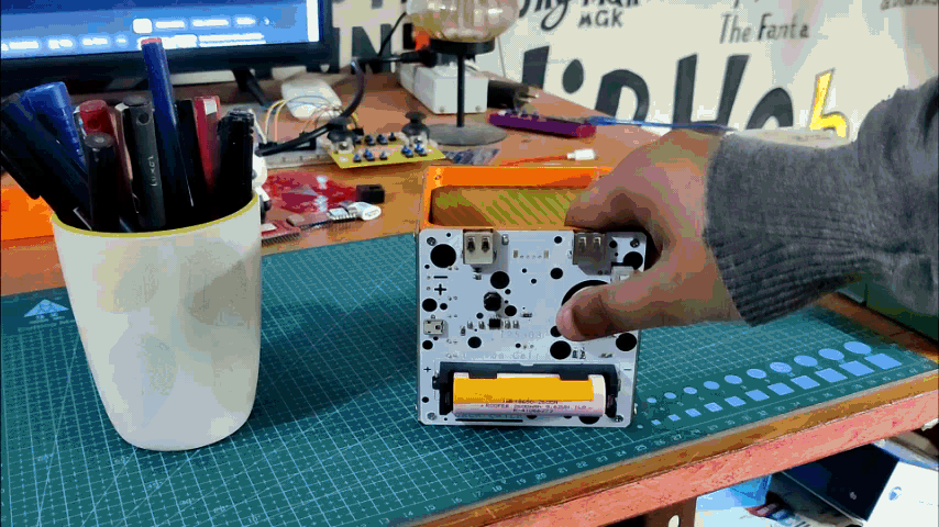
.gif)
- The assembly of the pen holder is quite easy; using four M2 screws, we first tighten the back PCB to the base and the 3D-printed PCB holder.
- Next, using 12 additional M2 screws—four for each side—we attach the final three Aesthetic PCBs to the Front, Left, and Right sides of the device.
End Result


Here is the final result of this crazy build: a Pen Holder created entirely out of PCBs.
This project tests the limits of using PCB as a material. Typically, PCB is used as a circuit board for XYZ electronics devices, but FR4 is a structurally sound material that can be used to prepare the body for some devices as well. In this case, PCBs were used as both the circuit and the body preparation, which is amazing.
This project is finished, and you can create your own using the attached files.
Overall, this was a worthwhile project that was far better than the mug pen holder I was previously using.
Thanks for getting this far; please leave a comment if you need any help with this project.
Special thanks to PCBWAY for supporting this project; do check them out for great PCB service at a lower cost.
Thanks again, and I will be back with a new project soon.