Next Gen Home Automation Using Eagle Cad ( Part 1 - PCB)
by ryan141298 in Circuits > Arduino
1393 Views, 2 Favorites, 0 Comments
Next Gen Home Automation Using Eagle Cad ( Part 1 - PCB)
Introduction:
- Why do i say its next generation: because it uses some components which are way better than traditional home automation devices.
- It can control appliances by:
- Google Voice Commands
- Touch Panel on the Device
- Control from app
- Control On and Off Along with speed of Fan
- Total Appliance:
- 2 On Off control devices
- 1 Dimming or Fan Speed Control
- How triac better than traditional relays
- No mechanical wear-out
- Easier to switch on zero-crossing. (Can also be done with a relay, but less accurate due to the switch-on delay)
- Can be used in dangerous environment, particularly in explosive sensitive environments where sparking relay contacts are absolutely out
- No EMI due to switching sparks/arcs
- No magnetic interaction with nearby inductors.
- Often more compact
- High frequency of switching
- It can control appliances by:
Components Required
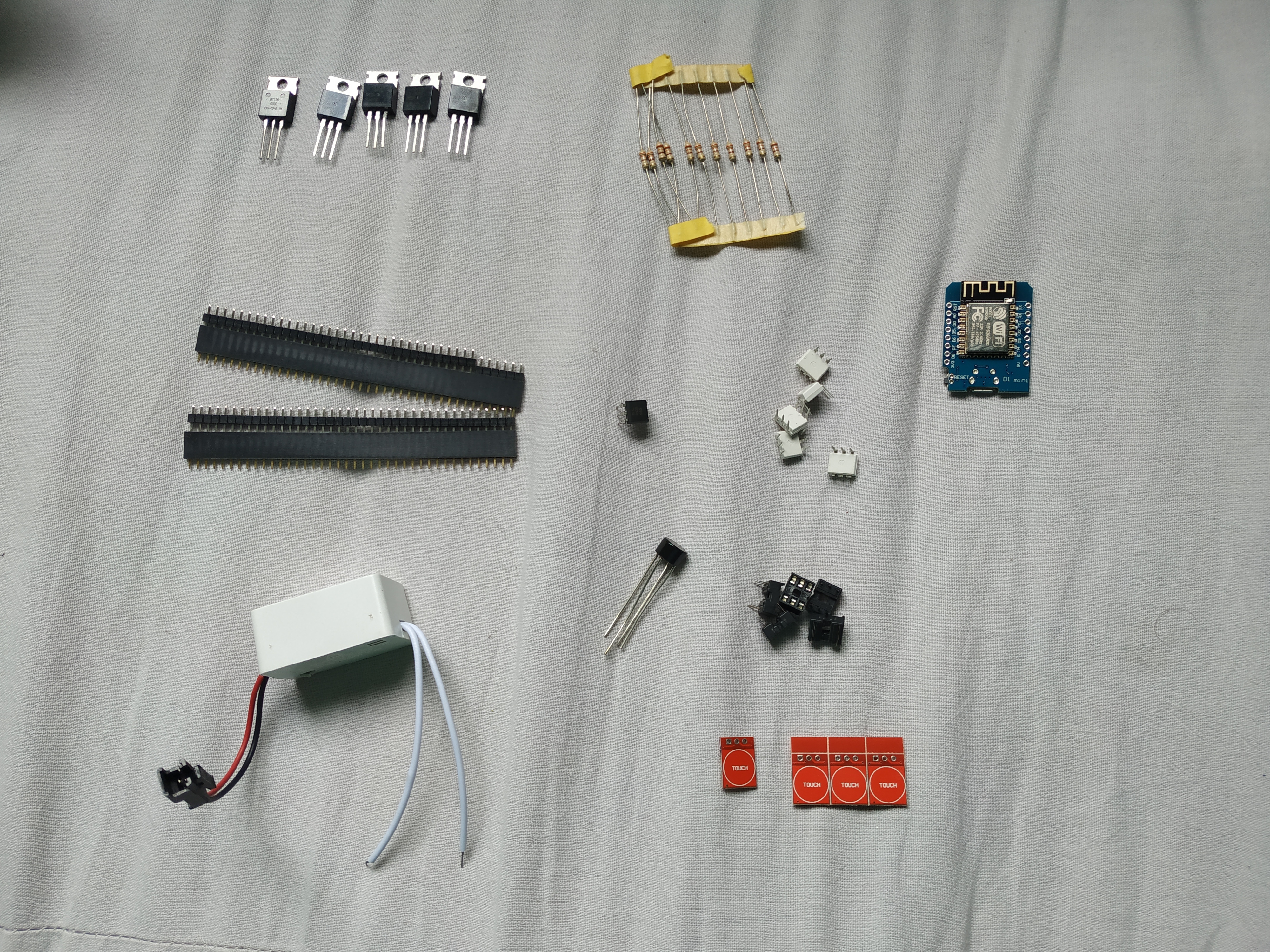
- Smps mini -5v
- MOC3041
- MOC3021
- Rectifier
- Triac-BT136
- Resistors
- Header Pins
- 4N35
- Touch Sensor
- D1 Mini Esp8266
Choosing of Microcontroller
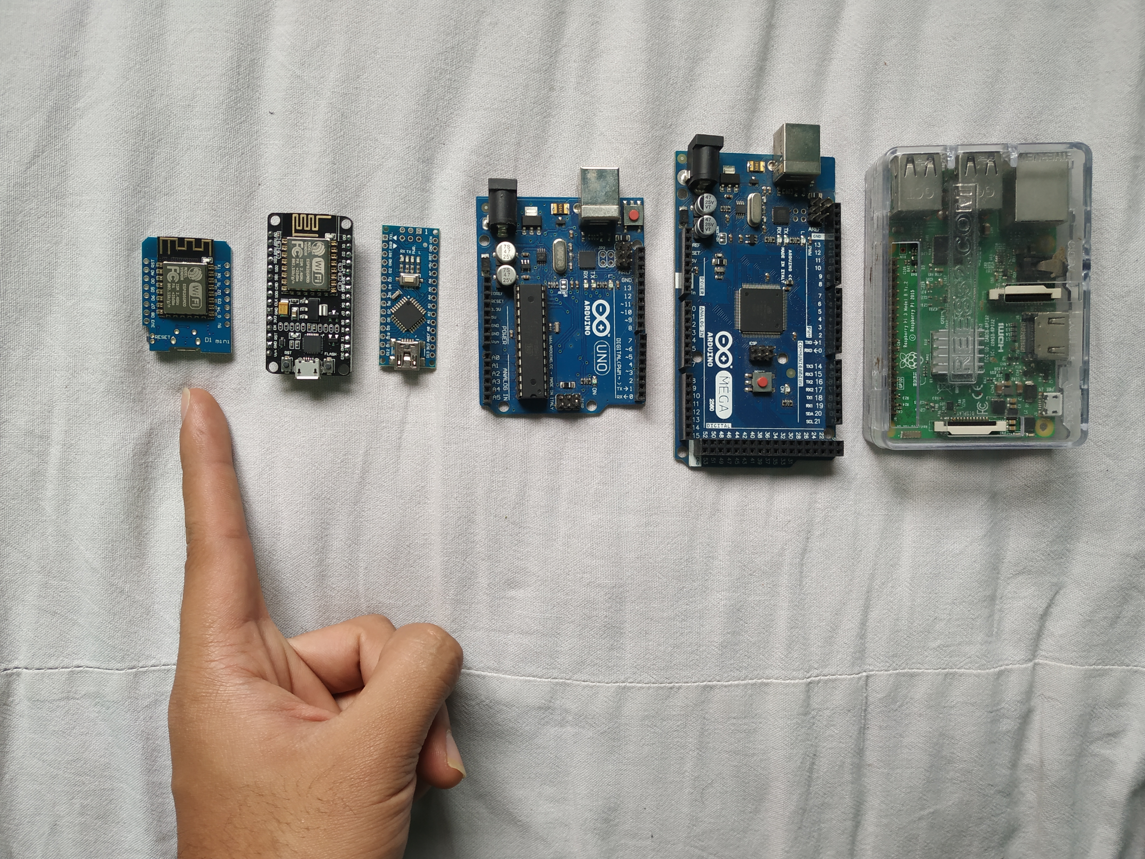
Which Micro controller to Choose:
We will be needing wifi control hence popular choices are either Raspberry Pi or Esp 8266.
As cost of raspberry pi is high, for this project i choosed Esp 8266. Now the question comes which variant of 8266?
- Esp-01
- Esp 12e
- NodeMCU
- D1 Mini
Now as i needed 10 controllable digital pins and size was an important factor i choosed D1 mini as it has sufficient no. of pins for my project and is small size.
PCB Designing Using Eagle Cad (Part -1)
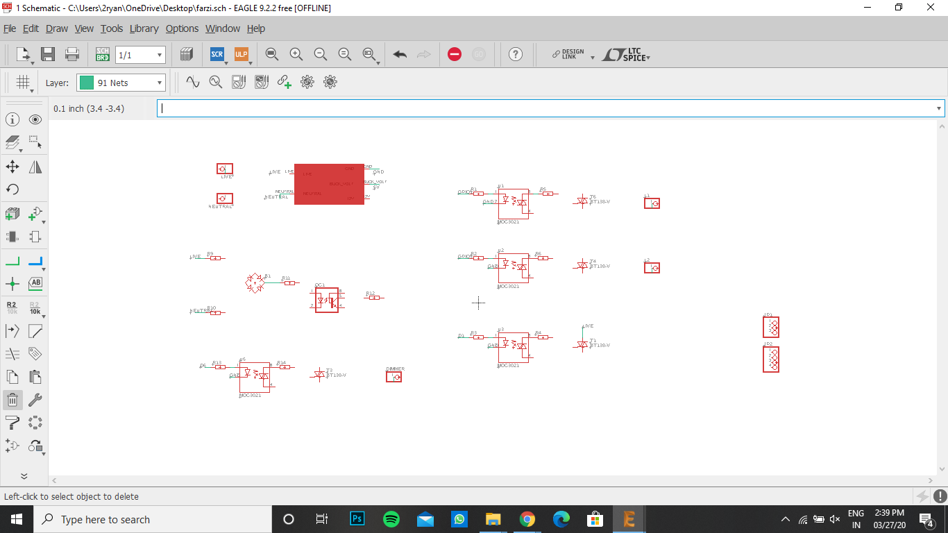
(Introduction):
- Open New Project, Name your project. Right click on it and select "New Schematic"
- Eagle Cad uses 2 files:
- Schematic file - For designing the circuit connections
- Board file- For final board design.
(Add Parts):
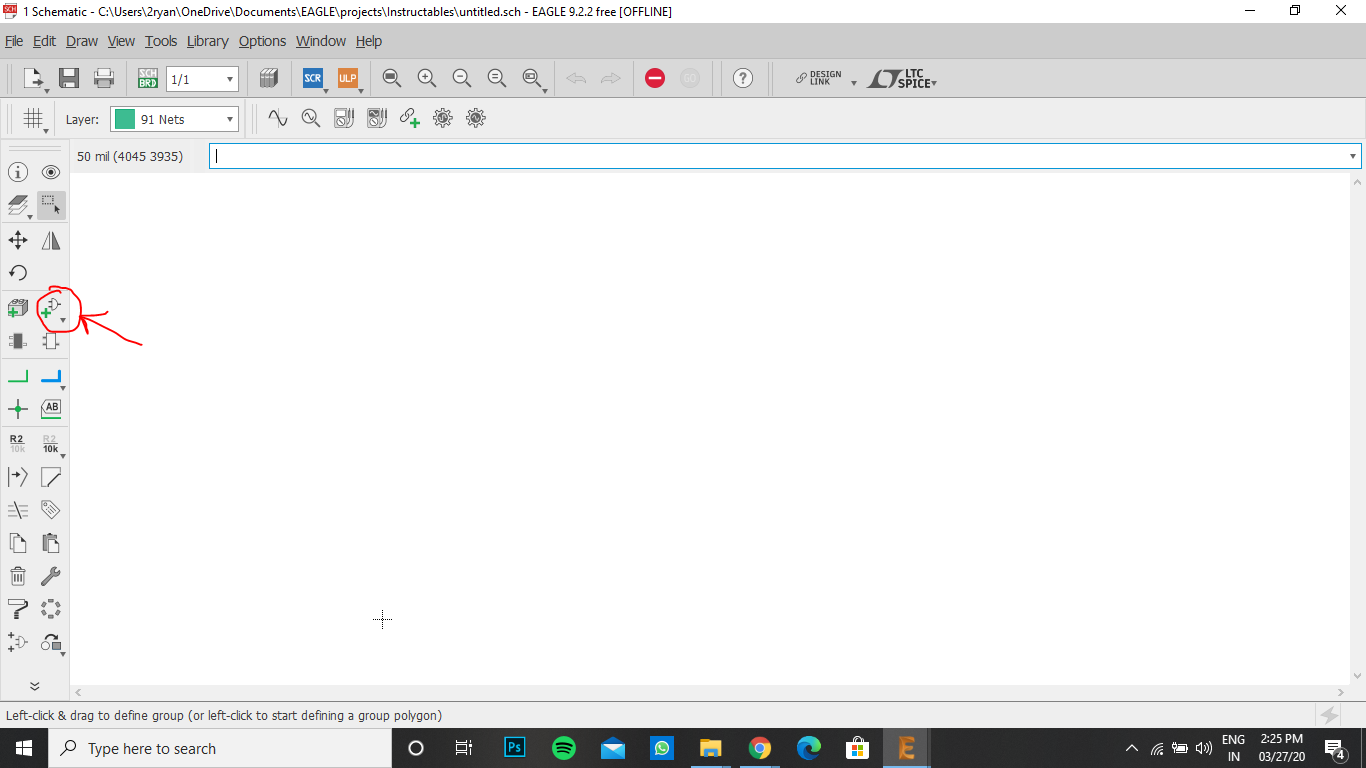
- Click "Add Part" as shown in the picture.
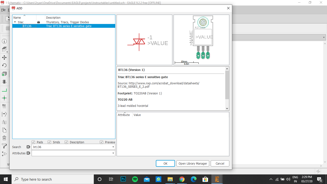
- Search each components and Press Ok.
- Place each components on the schematic.
PCB Designing Using Eagle Cad (Part -2)
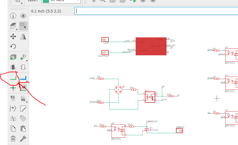
(Connect the components):
- According to the Circuit diagrams, each components should be wired accordingly.
- "Net Tool" is chosen and wires are made as shown in the picture.
PCB Designing Using Eagle Cad (Part -3)
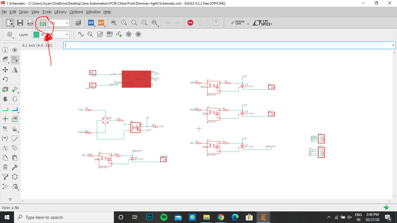
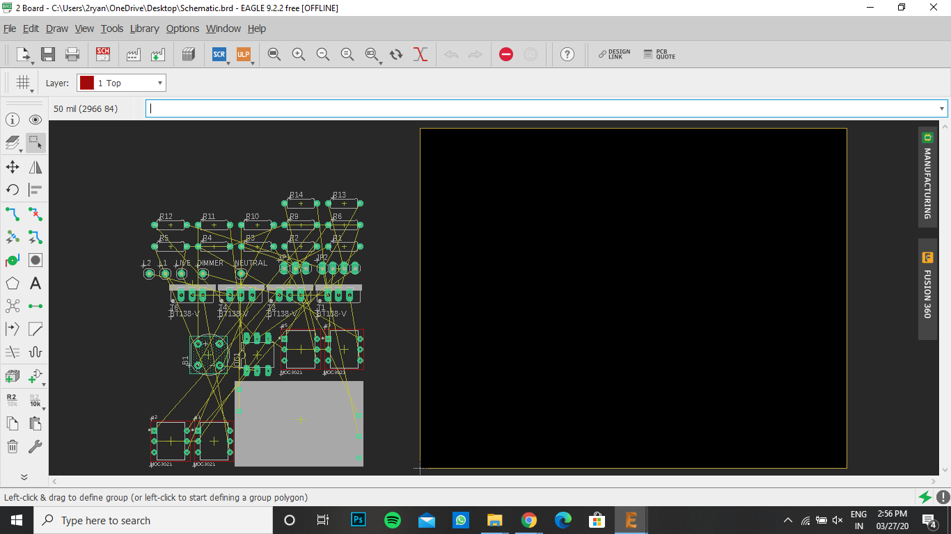
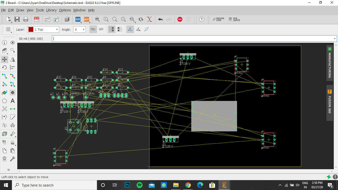
(Convert it to board file):
- Click "Generate to board" button on the left top as shown in the picture.
- Click "Create from schematic".
- Place the components as you wish to be on the final pcb.
PCB Designing Using Eagle Cad (Part - 4)
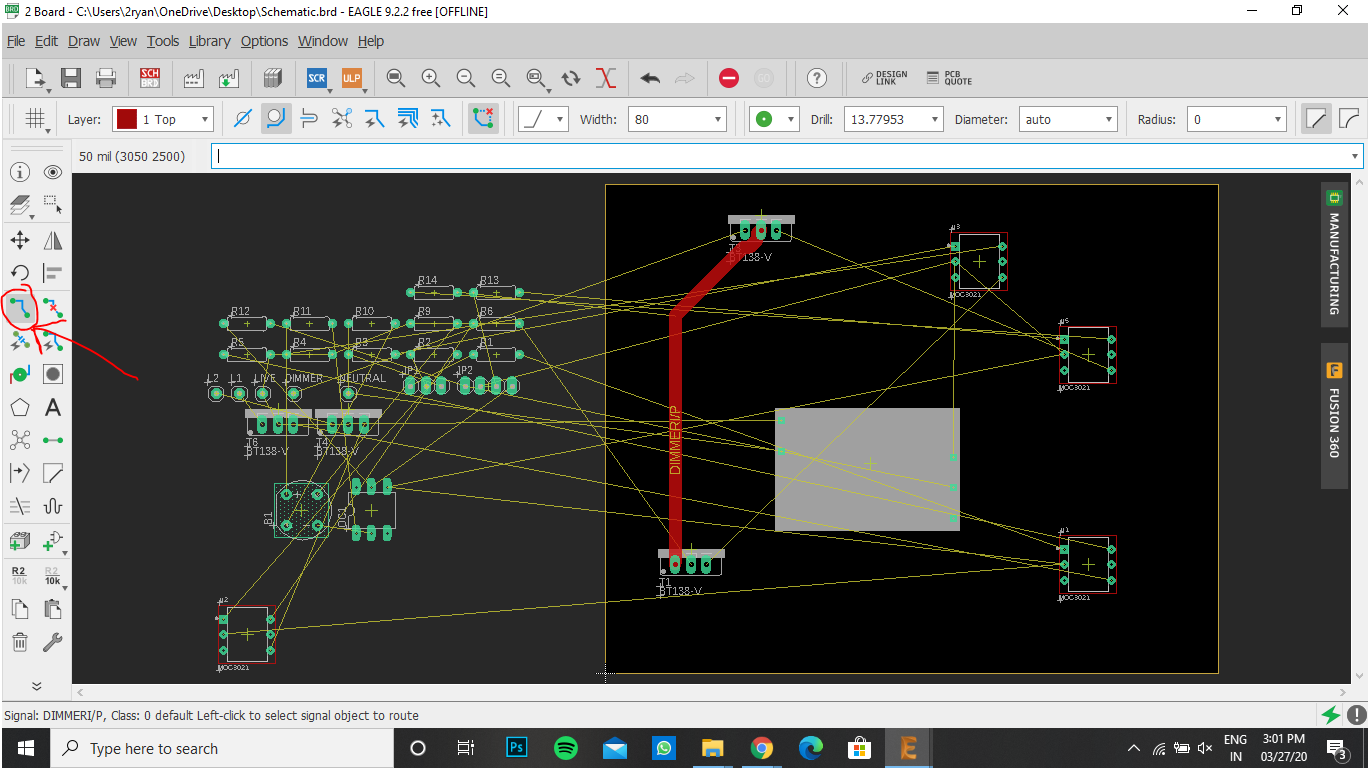
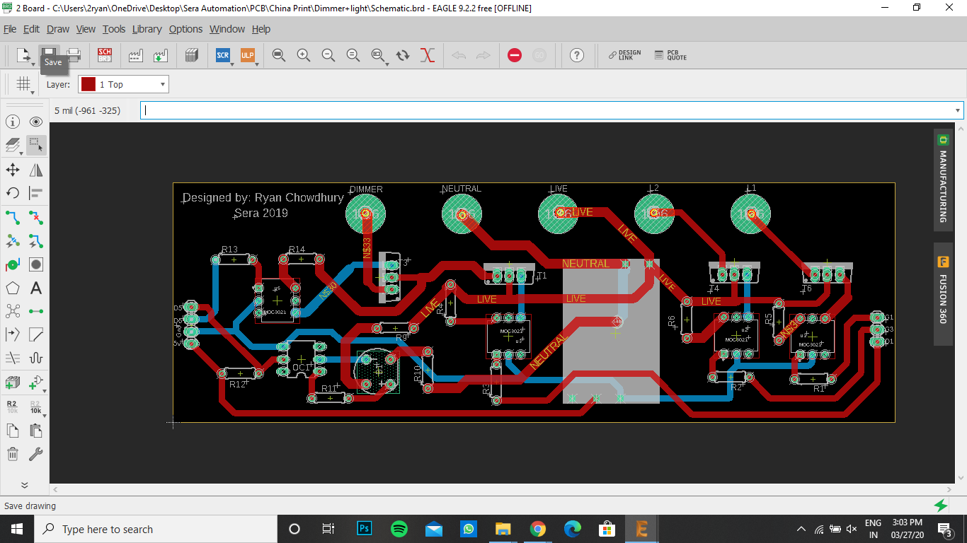
(Connections in the board):
- Use "Routing" tool to make the trace connections between the components.
PCB Designing Using Eagle Cad (Part - 5)

Generate Cam:
- PCB fabrication requires a lot of cam files.
- So by clicking on the "Generate Cam Data" button, the software will convert your project into files which can be read by CNC machines used for fabrication of pcb.
Testing PCB by Home Made PCBs
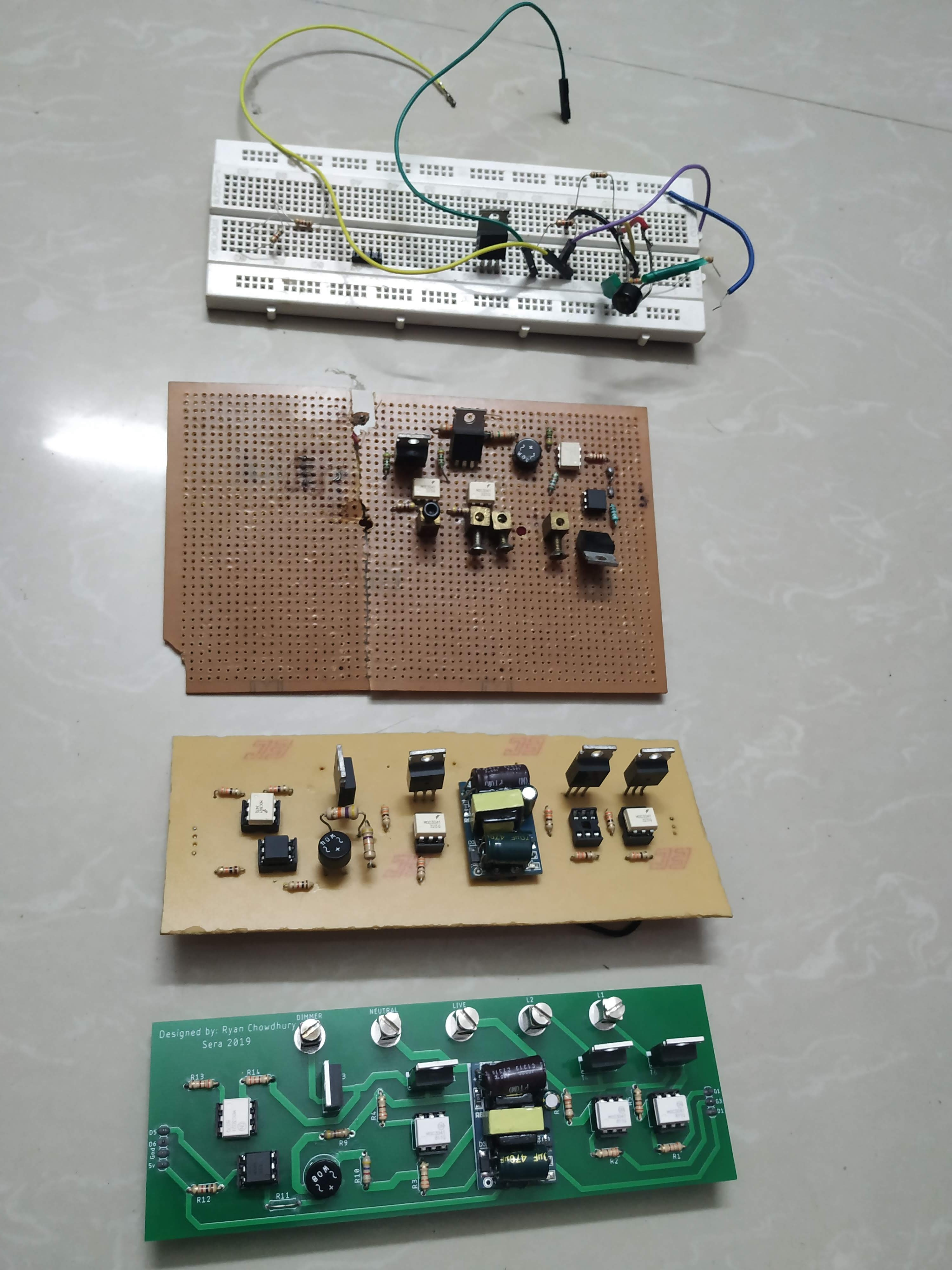
As cost of pcb fabrication is high, i wanted to check if its correct or not i made 3 similar circuit before sending it for fabrication.
- First one was done on the bread board.
- Second one was done by soldering components on stripboard ( or soldering board)
- Third one was done on the copper board by using the same pcb file and was made by cnc engraving present in my college campus.
After checking fully i send it for fabrication in PCB way
Check Gerber File and Send for Fabrication
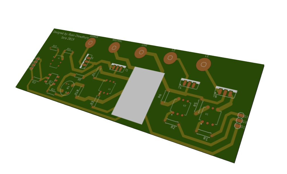
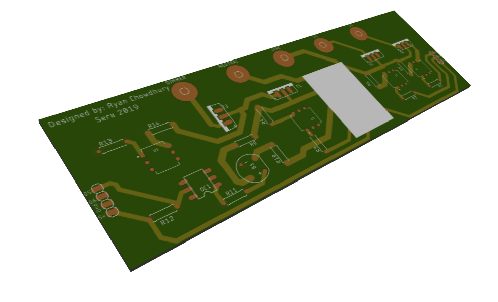
Checking:
- For Checking Gerber file go to : (http://mayhewlabs.com/3dpcb)
- Copy all the Gerber files and launch the gerber viewer
- Check How the final pcb will look.
Send for fabrication:
- I fabricated the pcb from (https://www.pcbway.com/)
Getting PCB and Soldering of Components
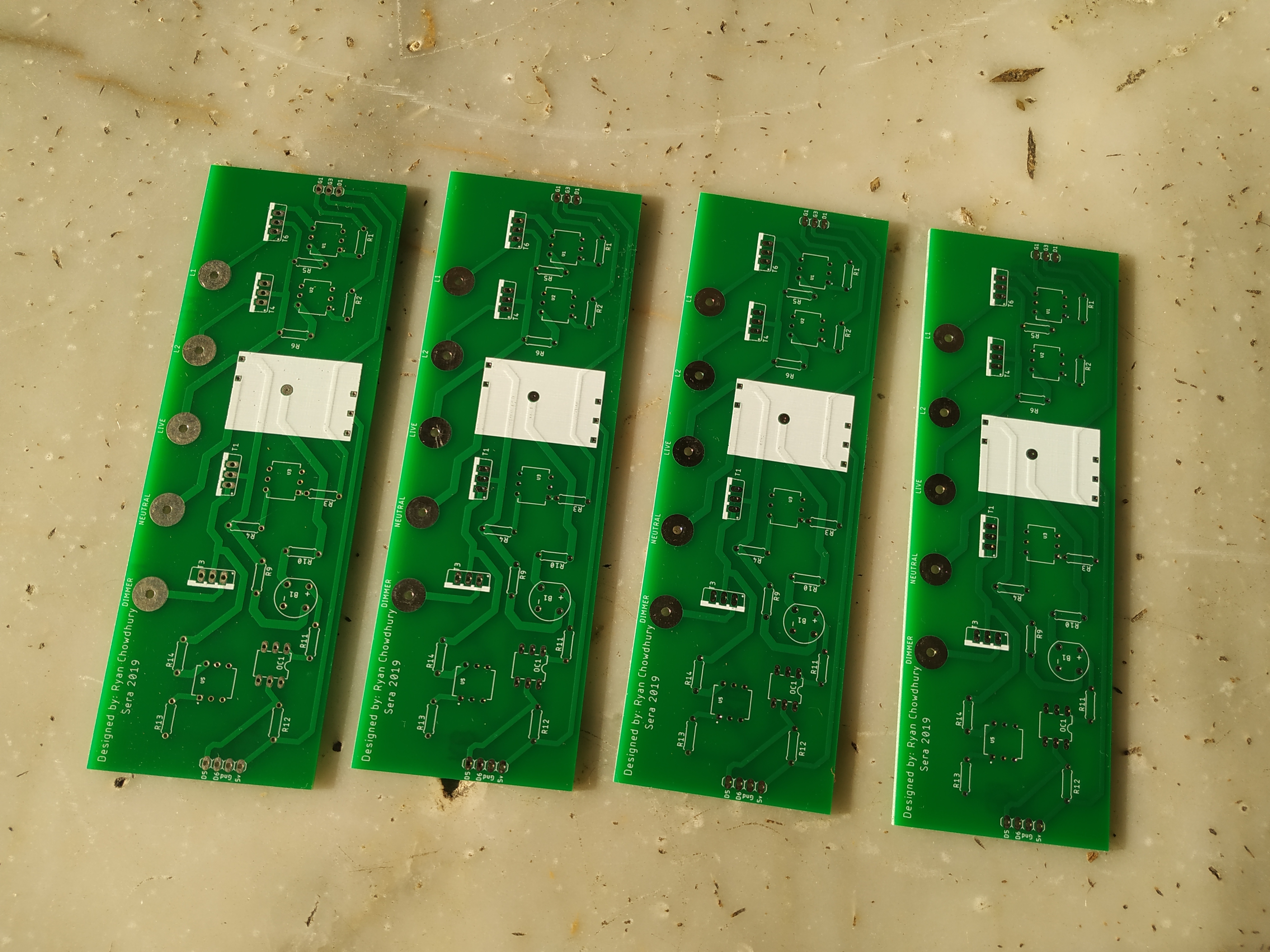
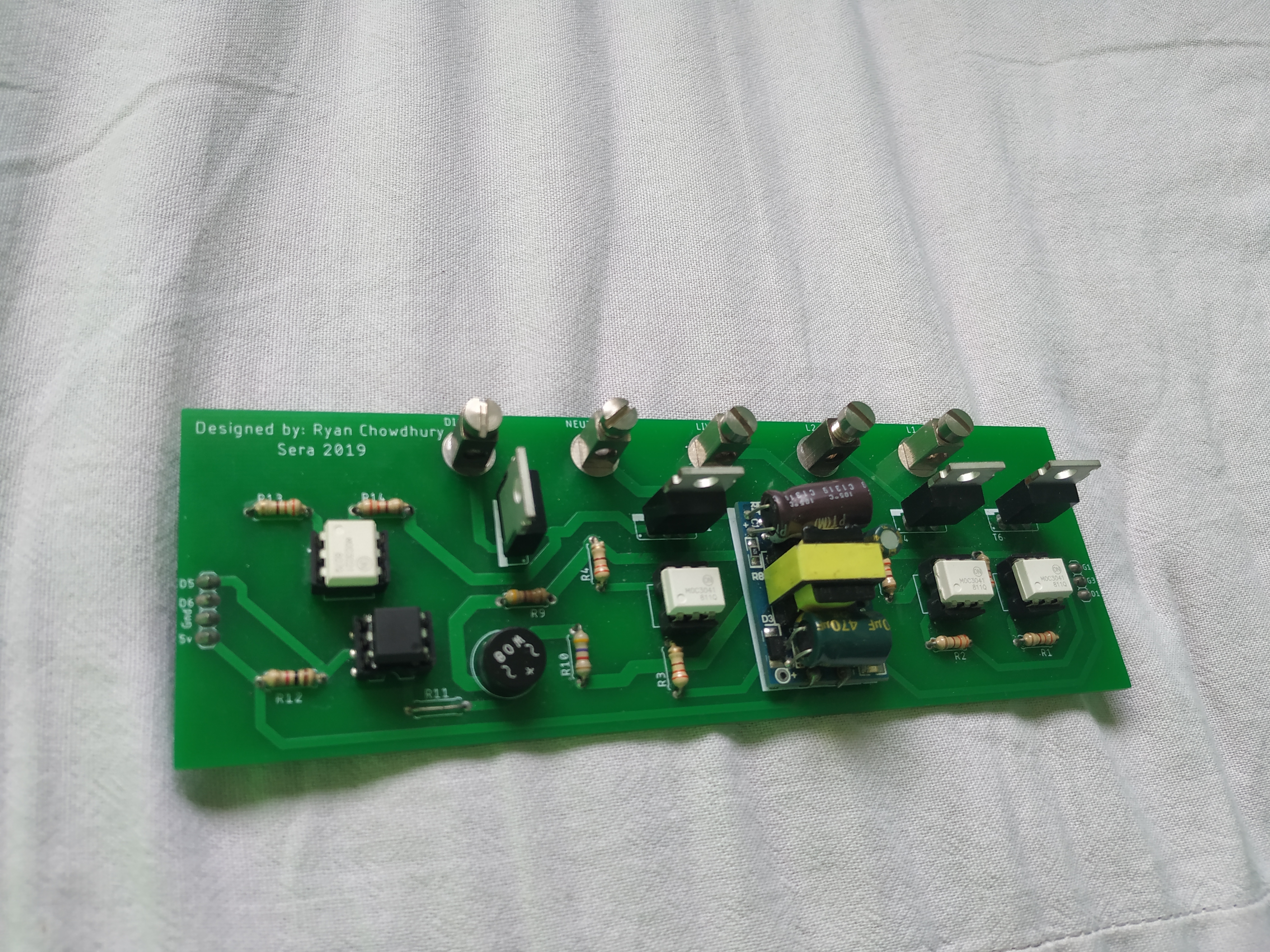
After getting the pcb, components are soldered and tested.
Touch Sensor and Microcontroller Layer
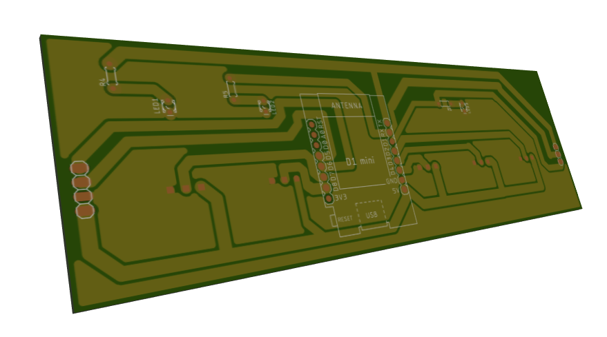
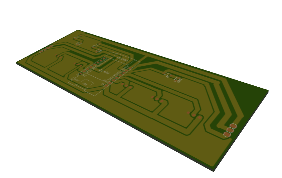
As this home automation project has touch capability, it require touch sensors. Hence we had to fabricate another pcb for touch sensor.This time I fabricated it in College CNC and not from PCB Way.
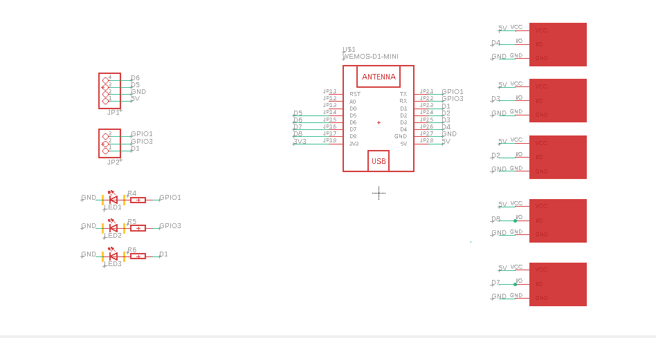
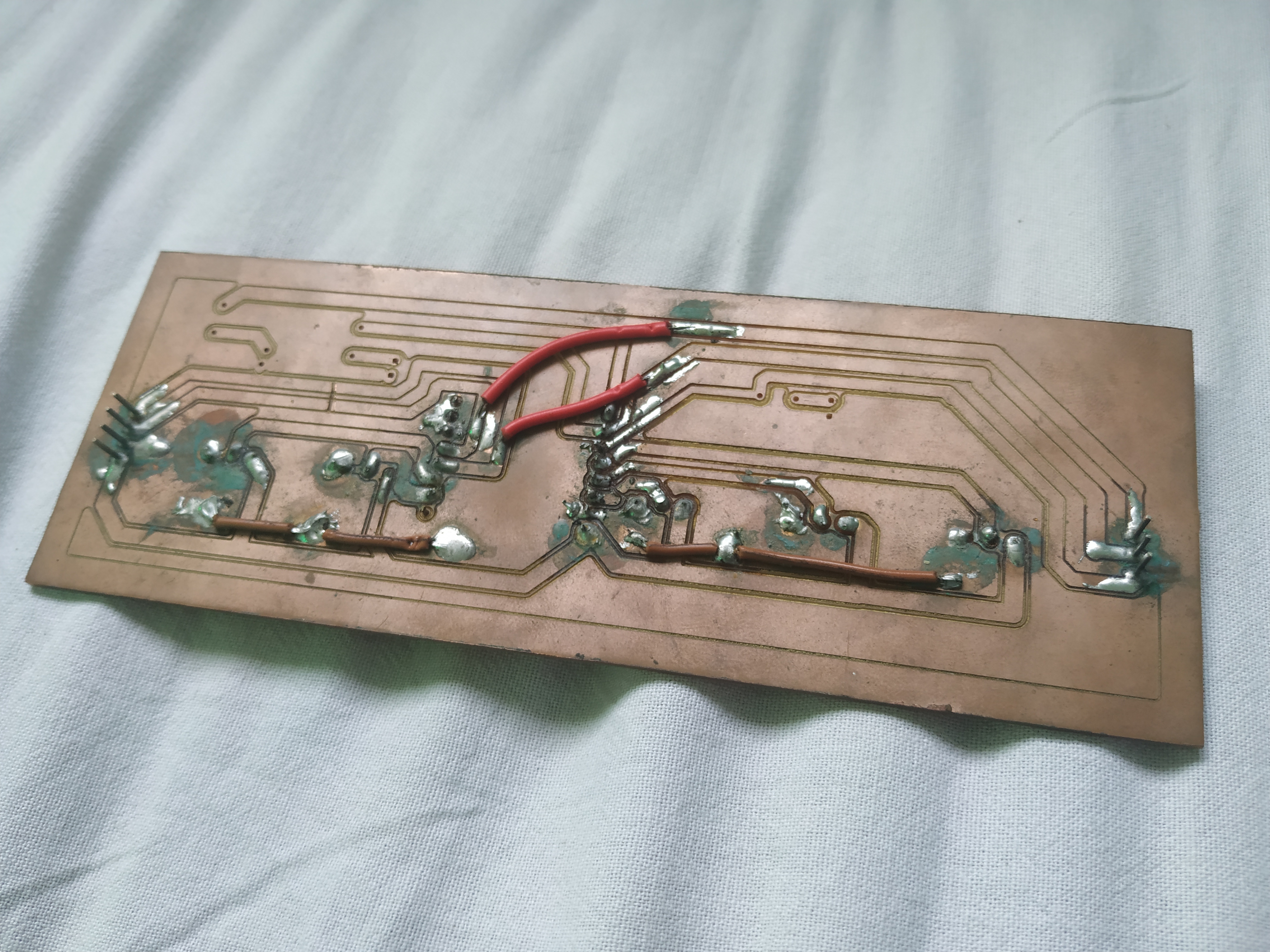
Schematic File and And Getting It Fabricated.
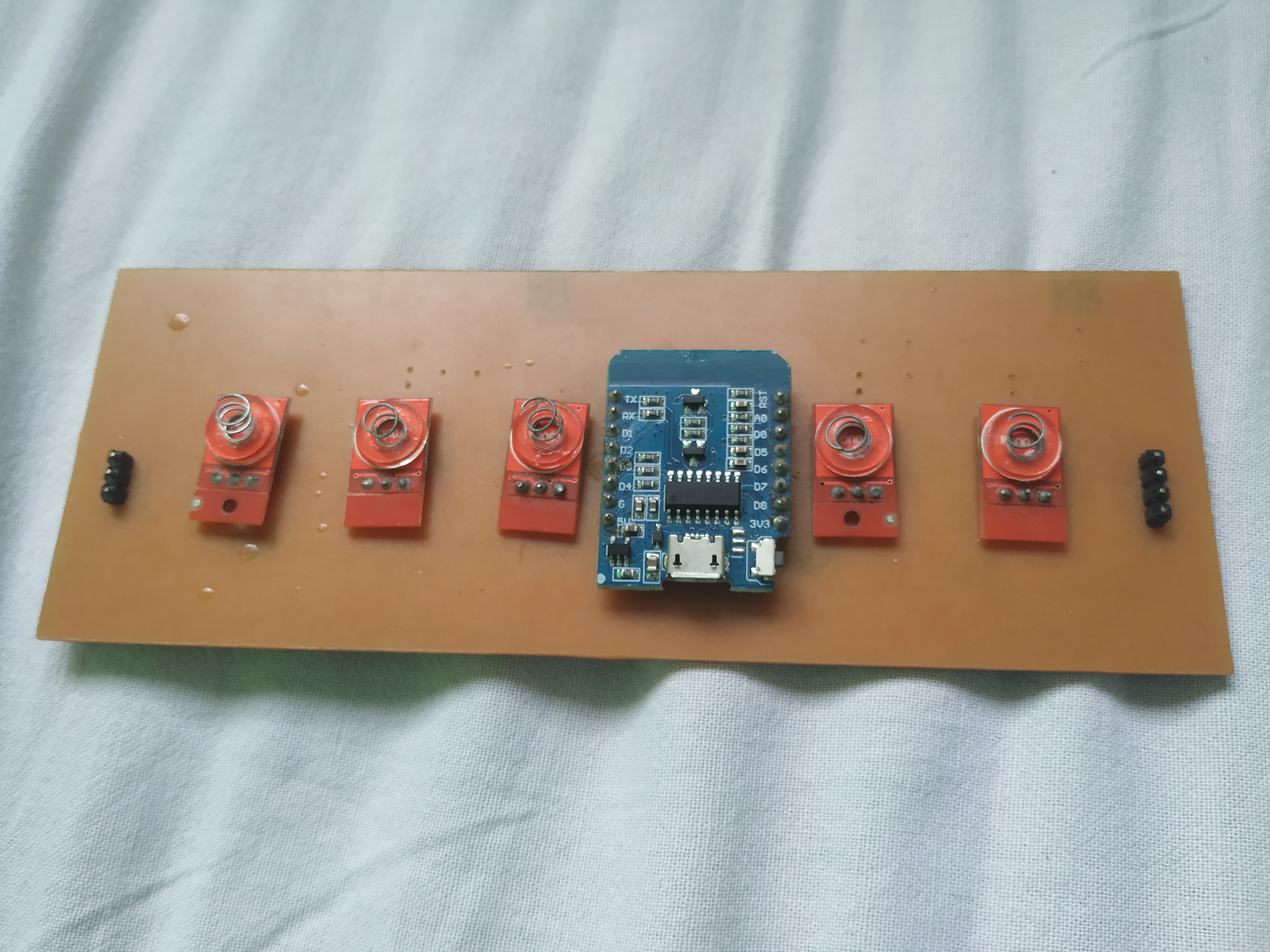
Finishing PCBs
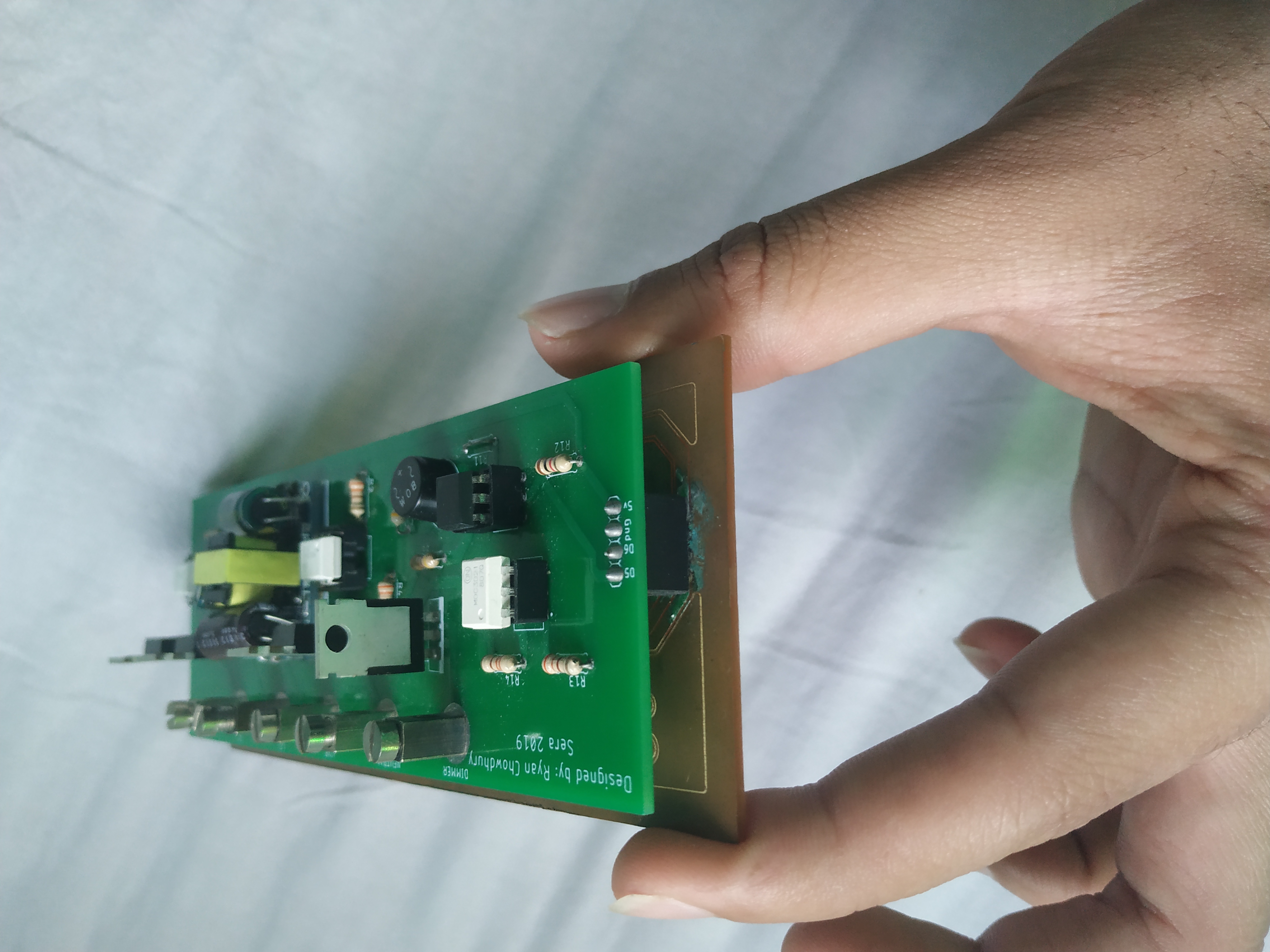
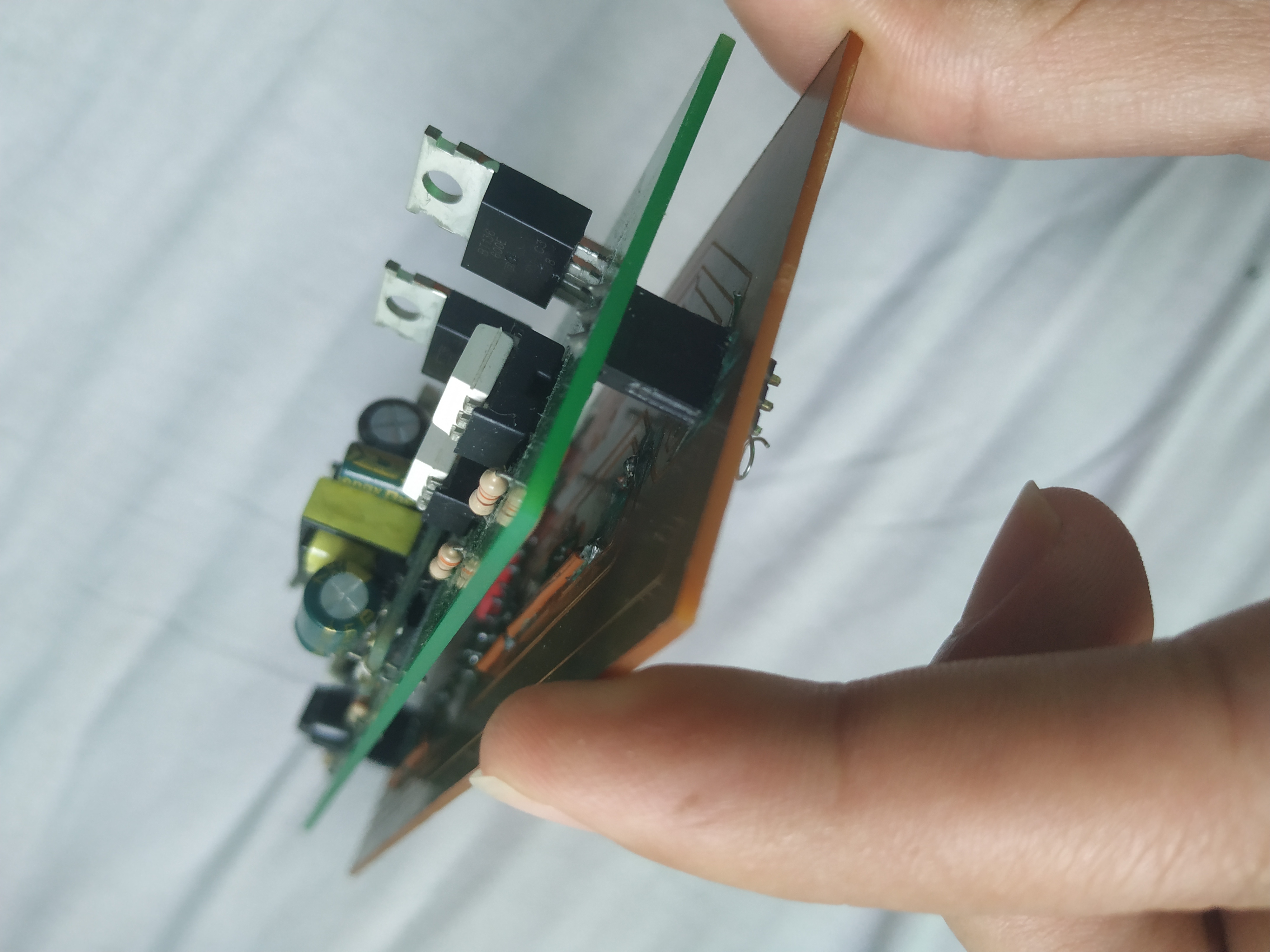
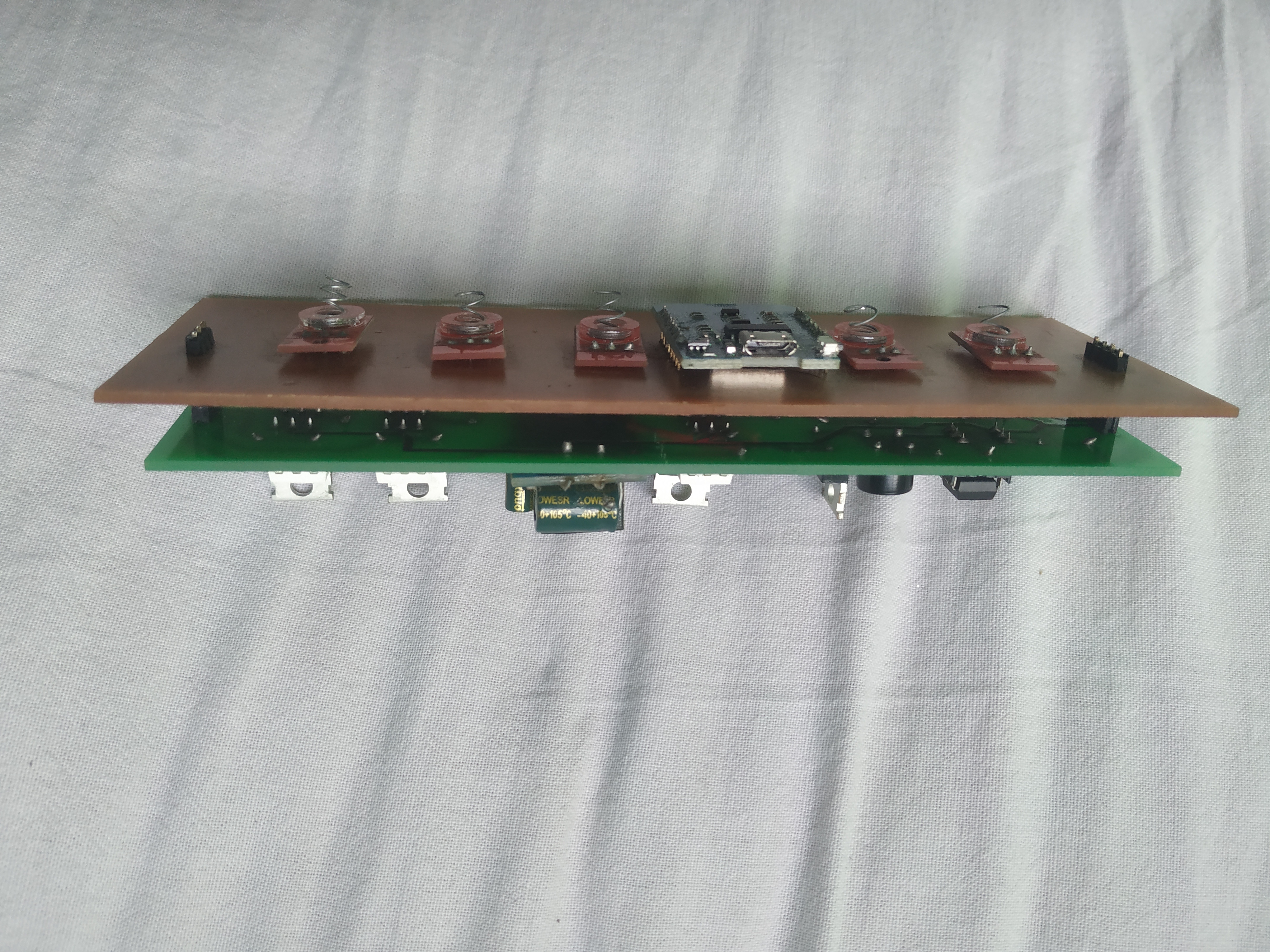
Both the layers are fixed one, top of another.
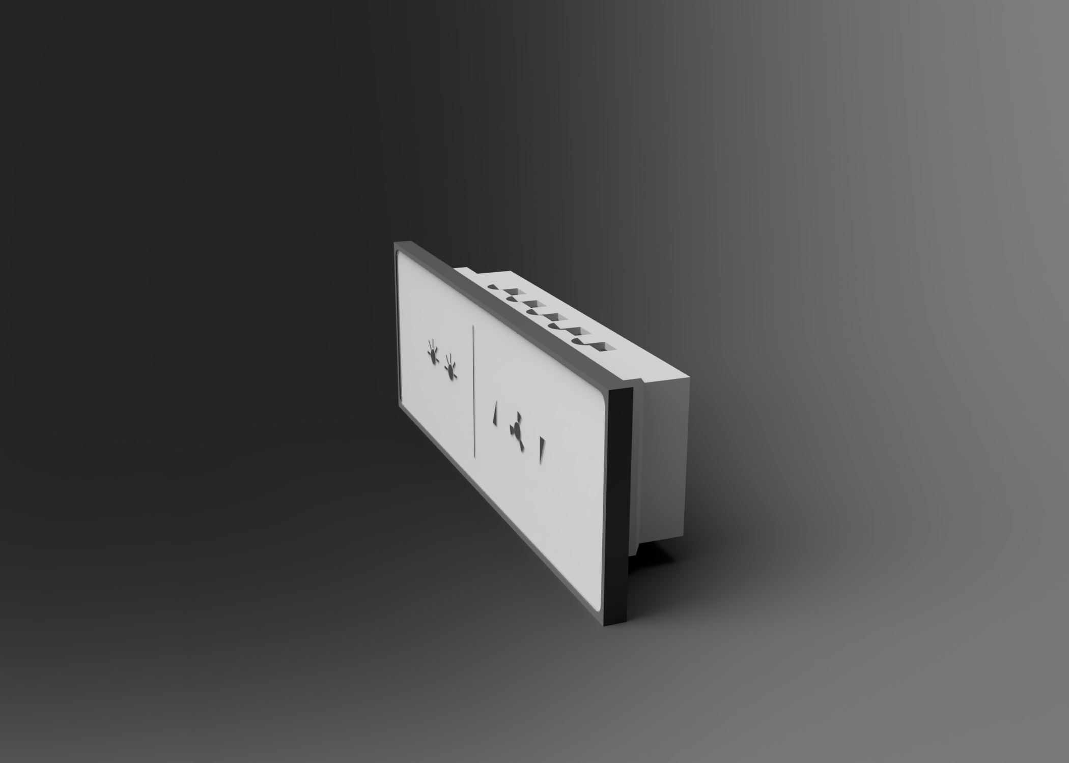
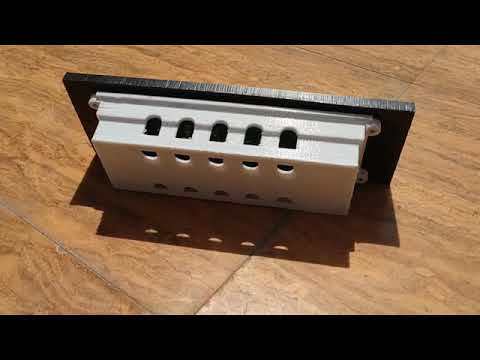
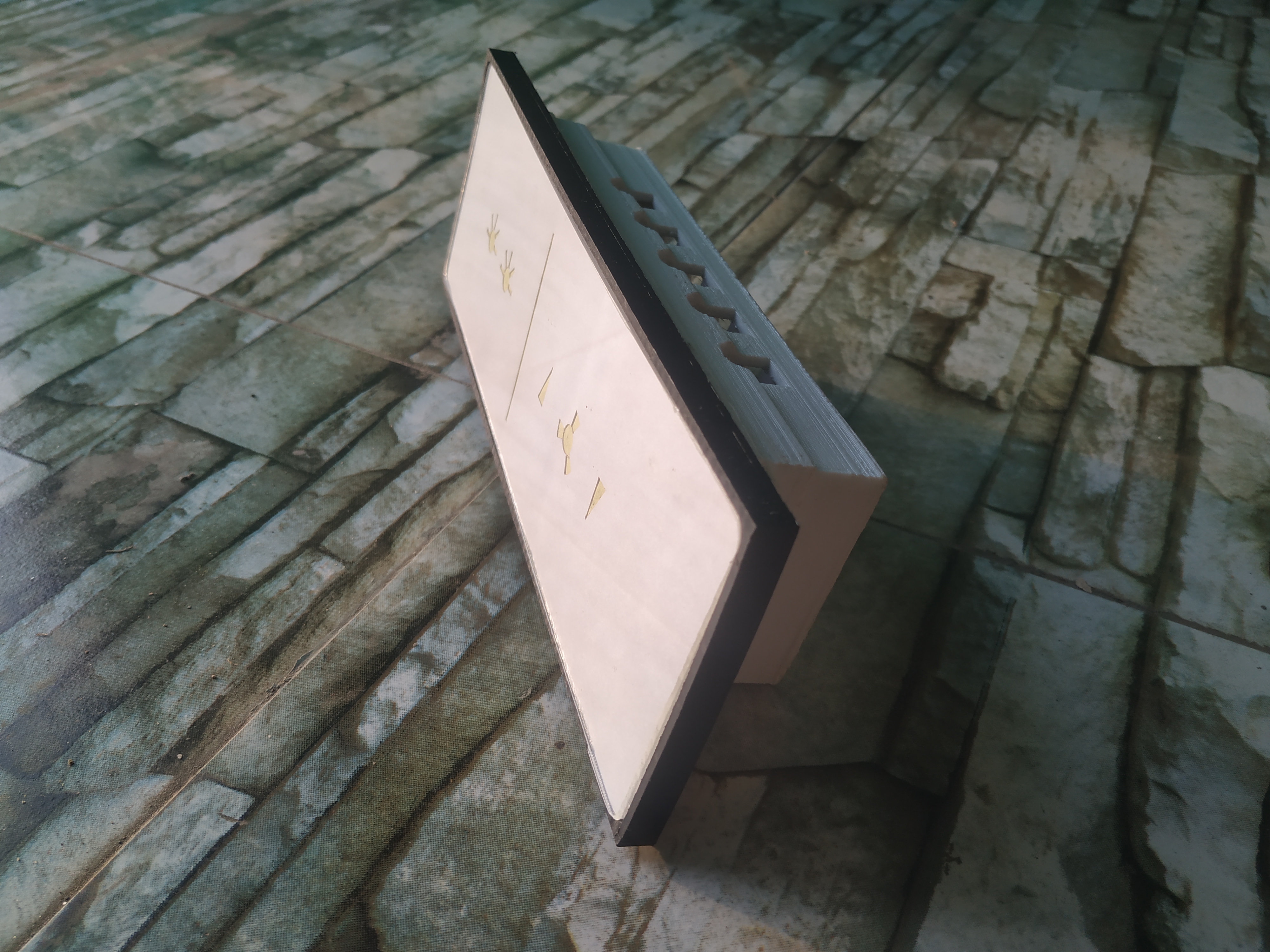
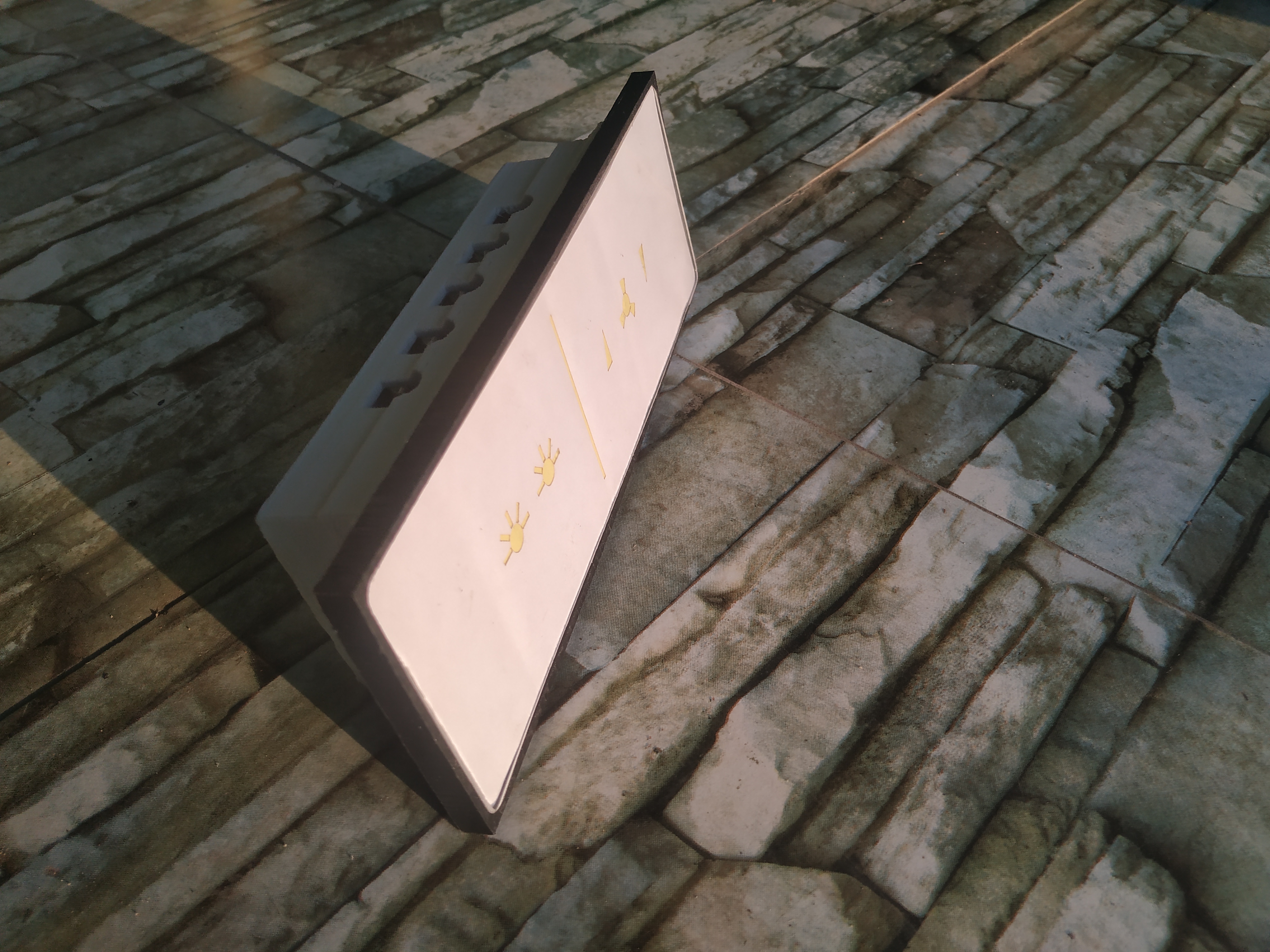
3d Printed Case
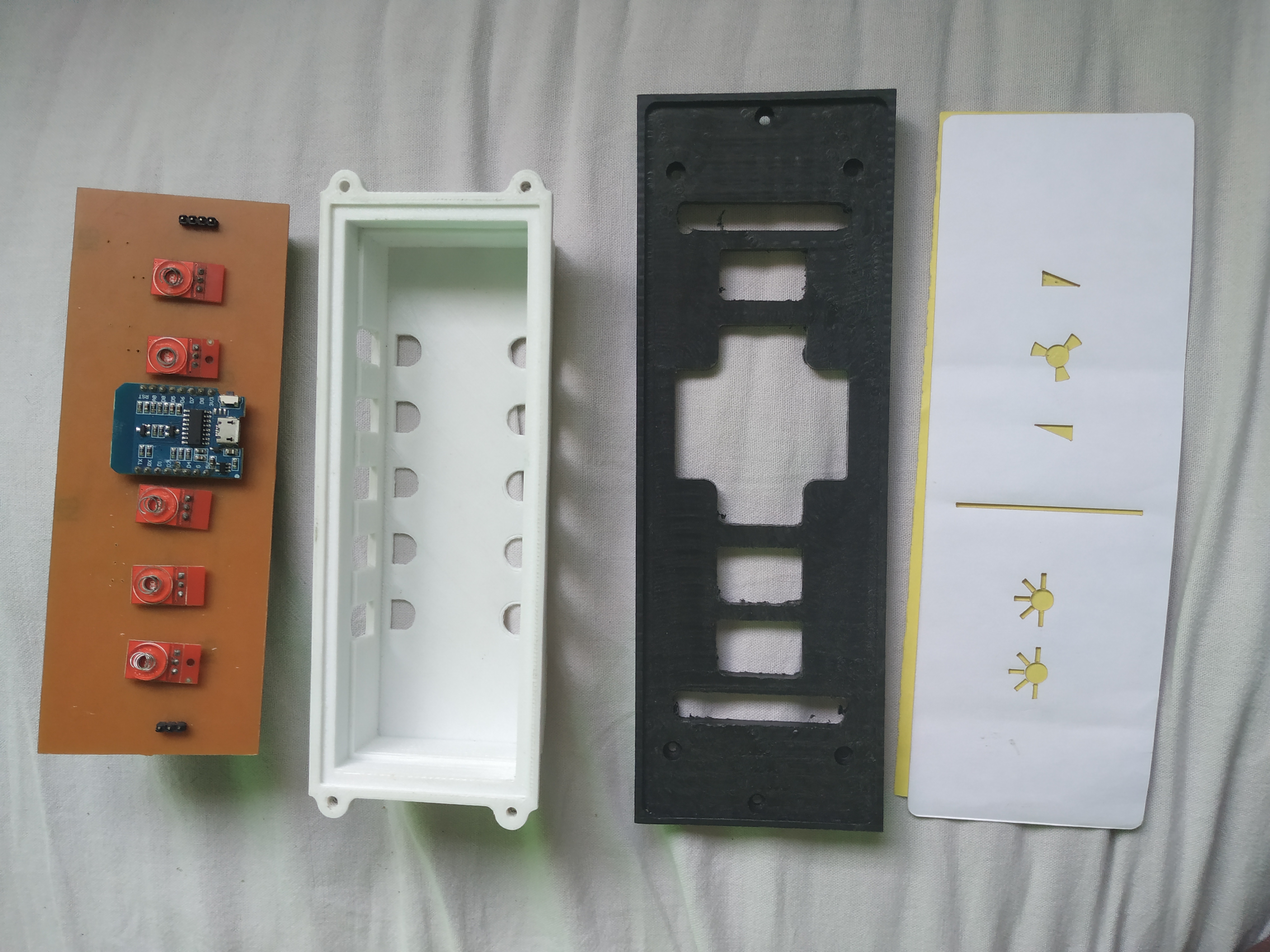
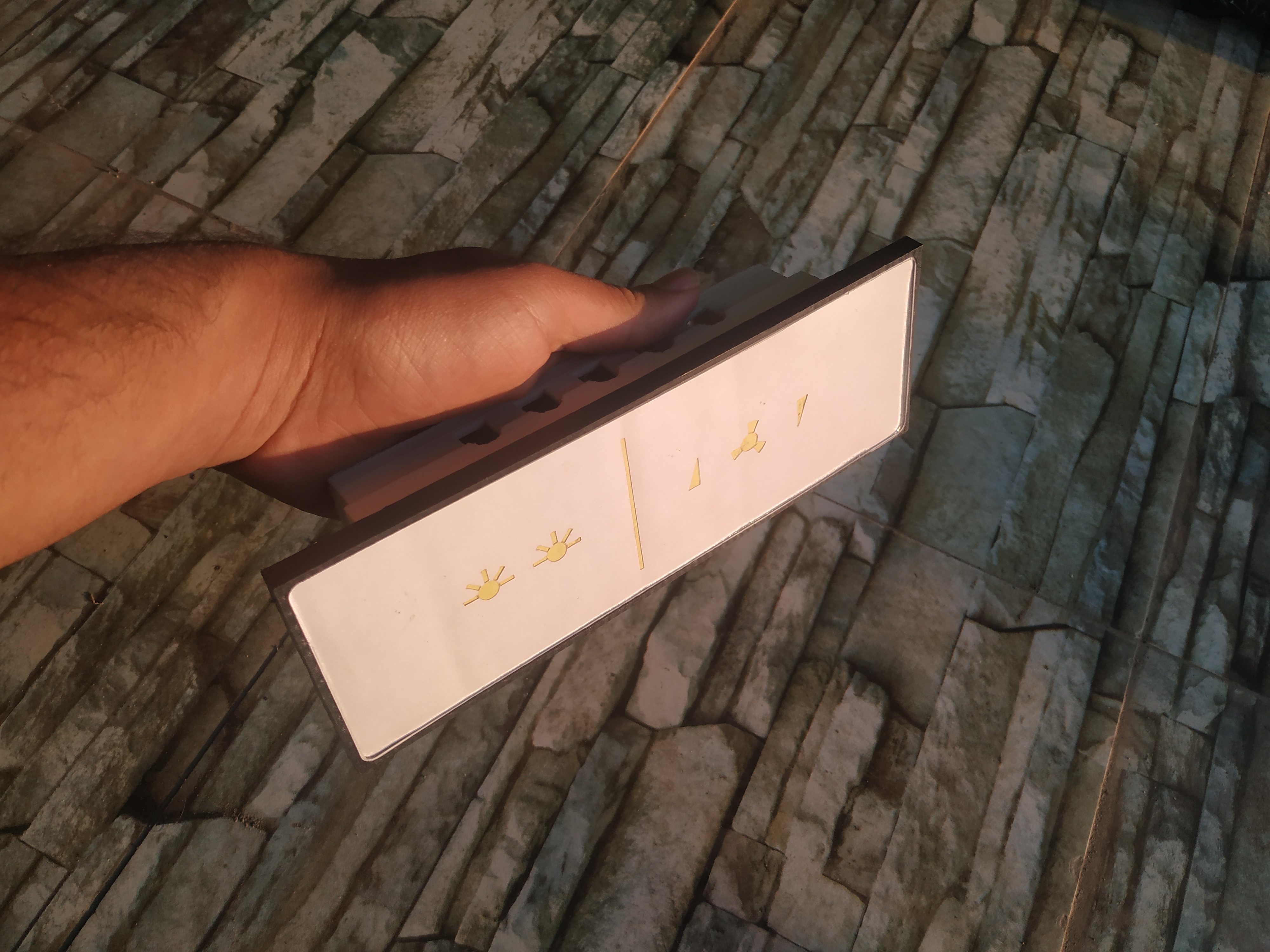
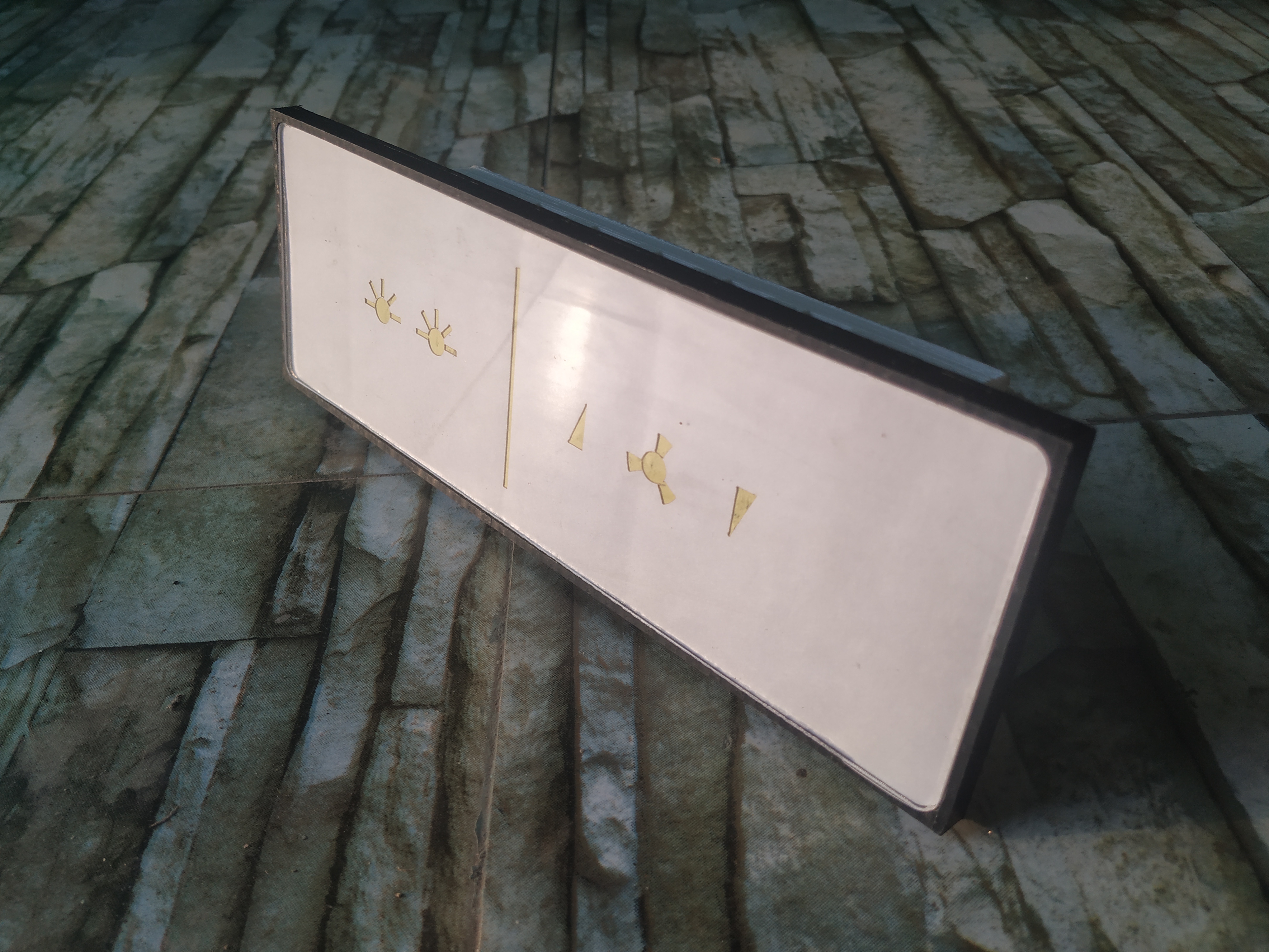
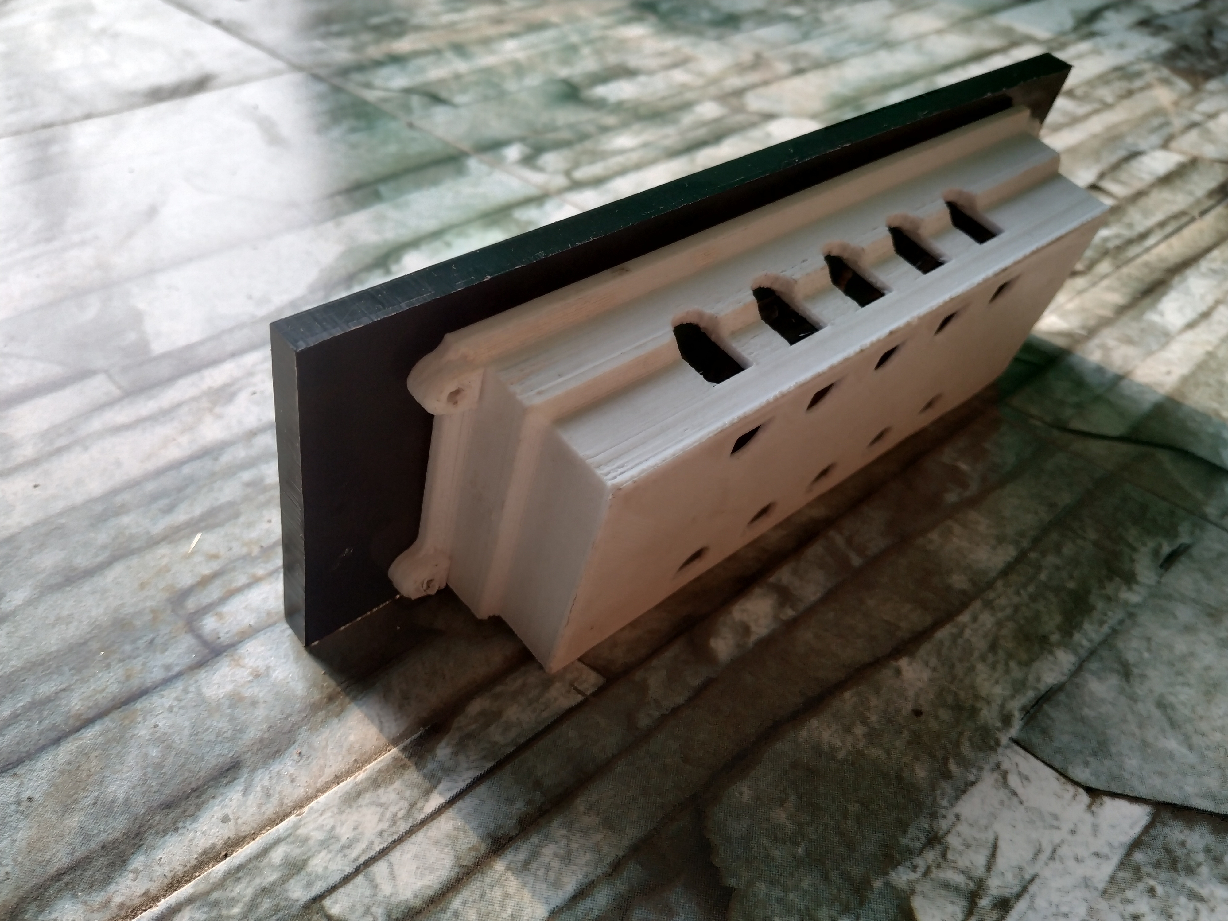
Casing is done by using 3d printer. Explanation of that would be on Part 2 of Instructables.