Making Paper Soldering Stencils for Electronic Circuit Boards by Hand
by JouleTime in Circuits > Soldering
7660 Views, 37 Favorites, 0 Comments
Making Paper Soldering Stencils for Electronic Circuit Boards by Hand
Easy because the small size make the leads heat quickly and draw in the solder. The solder is also drawn to the pads. This can help center and align the components. As the solder is pulled to the pads at either end, the part is slight shifted to balance the forces.
The hard part is the parts can be tiny and move around with the slightest touch. This can make it a challenge to position the parts and annoying because they move around just touching them with a soldering iron.
After learning to make my own aluminum stencils I decided that SMD parts, even with fine pitch pins like on a 32-pin TQFP, are really easy to use.
The secret is in the solder paste and how it works.
Solder Paste, Right Amount Is Most Important
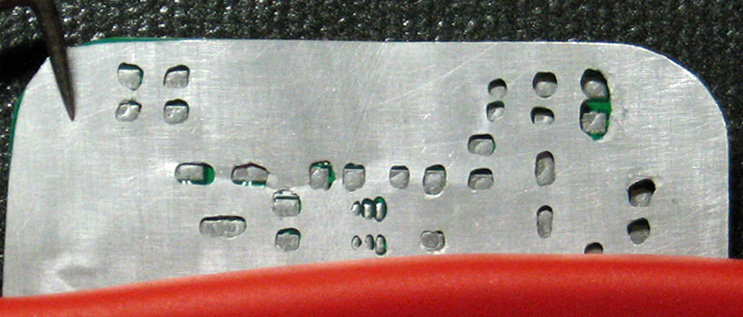
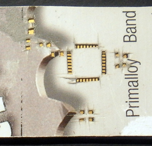
Solder paste is thick. When it is cold, it can hold its shape. When you first apply the paste it will look nice and each pad will have an individual patch. Then as it warms up the paste will flow. A part with many pins will become a grey blob.
It does not matter if the solder paste is a blob instead of individual patches. Magically as it is heated, the paste for individual pins will form distinct patterns to match the pads and pins.
I learned that it was more important to have the right amount of paste, and less important about how nicely it was applied. Too much paste and it would create solder bridges for me to fix. Too little paste, and either a bad connection or the whole part could be drawn to the opposite pad.
Aluminum Stencils Are Tricky
At first I would etch stencils out of aluminum. I tried to make them a perfect match for the part, but it never worked out perfectly. The biggest problem was that etching a hole through a large pad took longer than etching a narrow slot. My narrow slots would be over etched by the time the rest of the board was done.
Here is my Instructables on Aluminum Stencils: https://www.instructables.com/id/Easy-Aluminum-Solder-Mask/
Success varied with each attempt, but even the bad stencils worked. The thing I learned is that if the stencil was over etched, then I needed to scrape away the extra solder to keep the melted solder from forming bridges.
Switch From Aluminum to Paper Stencils
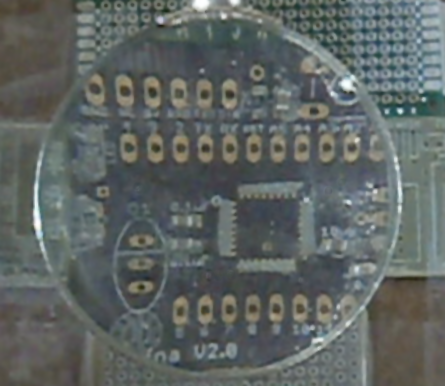
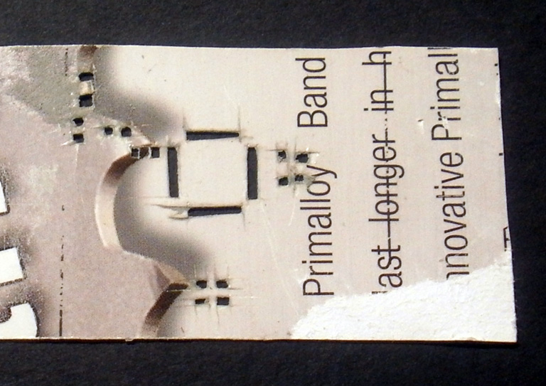
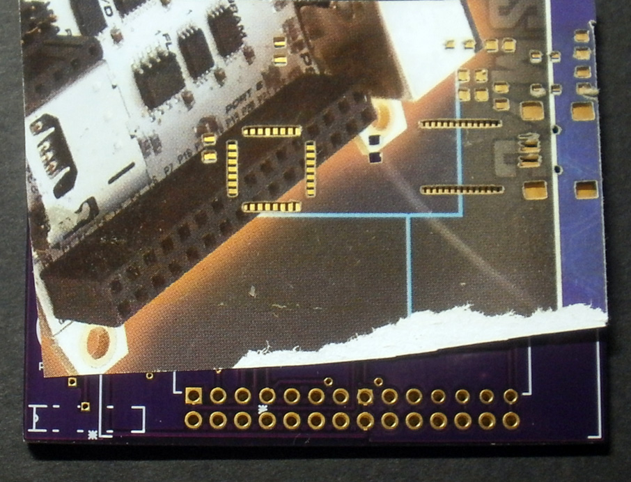
Then I had an inspiration* to use paper instead of aluminum for my stencil. Coated paper can come in the right thickness (I first tried gloss magazine cover paper). Paper can be cut out with an X-acto knife with fair precision. But there was no way I could cut out every pin for a 32-pin TQFP profile on a stencil.
To understand the problem, find a mechanical pencil. The typical pencil lead is 0.5mm thick. The pin size for a 32-pin TQFP package is 0.3mm. There is no easy way to cut out by hand 32 slots thinner than a pencil lead and have them look good. The secret is why bother.
Since the solder paste is going to flow and spread out, why not cut a long slot to take the place of many small slits. It works but you have to make adjustments.
* Others had the same idea before me, http://www.sharebrained.com/2011/01/11/pcb-stencils-on-the-cheap-kinda/.
Change From EagleCAD to PDF
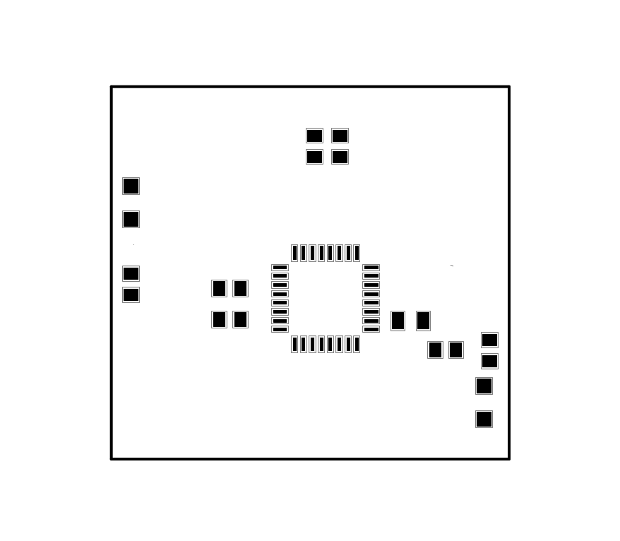
When I make a stencil, I start with my EagleCAD file for the board. I turn off all the layers except for dimension and tcream. Then I open the Design Rules popup window, and select masks tab. I set Cream Min to 4mil, 80%, and Max 5 mil. That helps to reduce the amount of paste that is applied to each pad. This minimizes the likelihood of creating solder bridges on closely space pins. (These are the same rules I used for aluminum stencils.)
From EagleCAD, I print the board image as a pdf at a 1 to 1 scale. This allows me to open the image and edit any details.
The image is opened in either Gimp or Photoshop. The resolution is set to at least 400 pixels/inch. The image is cropped with about 1/2” of space left around the stencil.
Print and Check Scale
At this point you should print a copy and measure the size of the board and compare to the size that it is supposed to be in EagleCAD. Scale the image as needed to match the correct dimensions and save the as either a jpg or png file.
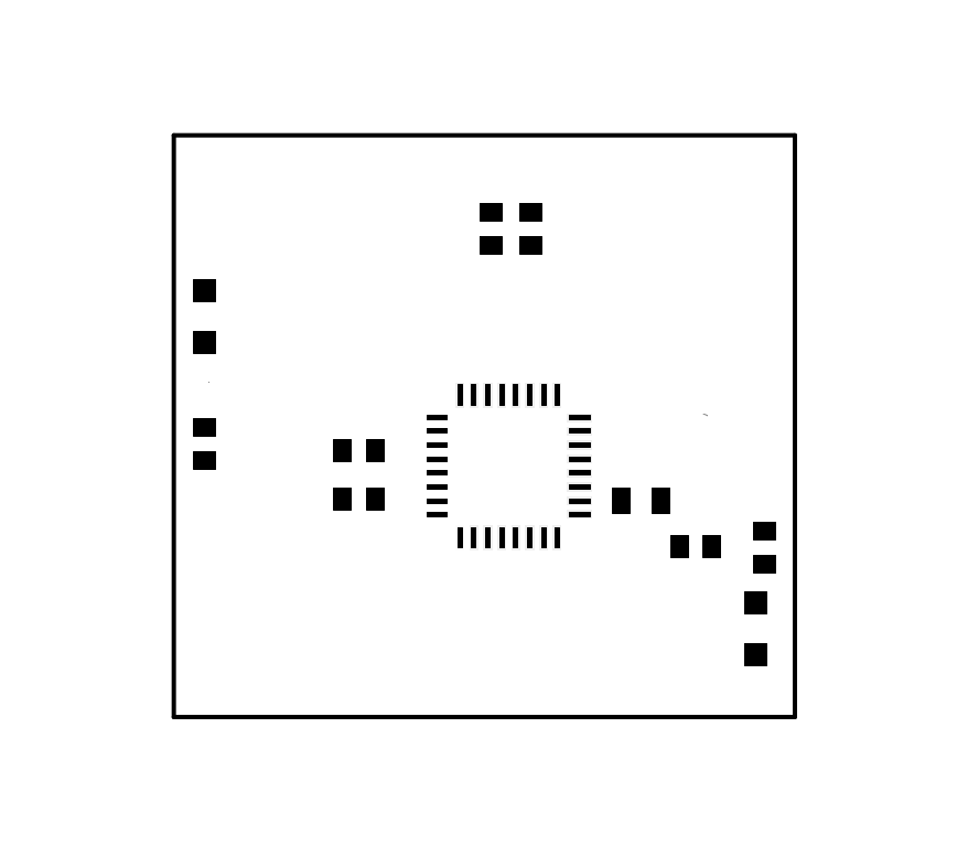
The pads for resistors and other similar parts were shrunk when you adjusted the Design Rules, but the stencil shape for a multi-pin part, like a microcontroller, need to be fixed.
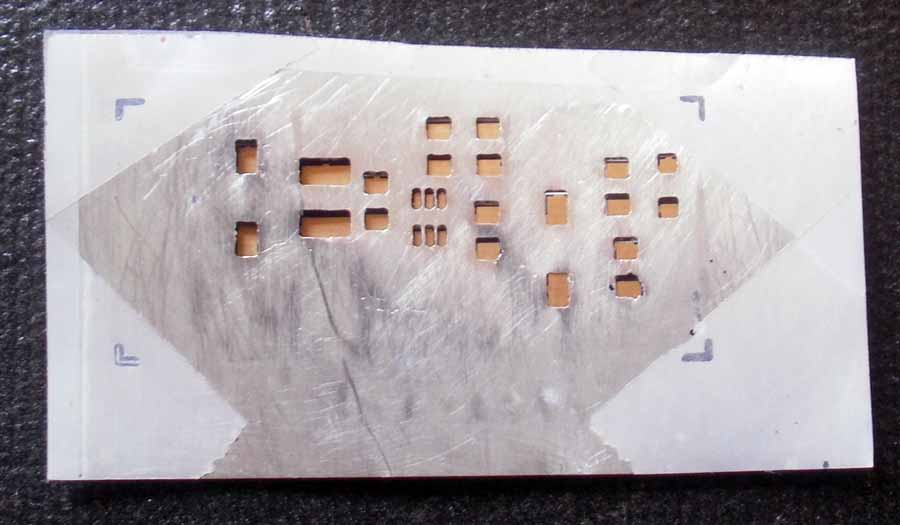
Remove Top and Bottom From Row
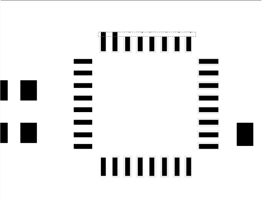
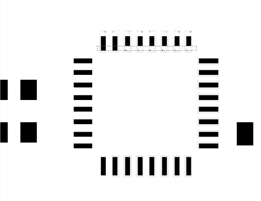
I start my removing part of the top and bottom of each pin. You should erase or white out slightly less than a third of the pin from the top and bottom. You can use the eraser tool, or pencil tool with the color set to white, or select the area and use the paint bucket tool.
I found the paint bucket worked the best. Start by selecting the top of a row of pin outlines. Then select white as the fill color. Bring the paint bucket tool over each pin and click. The selected area of each pin turns white. You move down the row fixing each pin outline. When the top half is done, you repeat for the bottom half of the row of pin outlines.
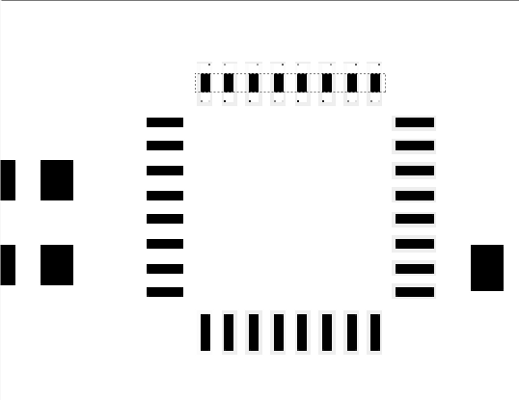
Fill in Between the Pins
Now you have about the middle third of the pin outlines left. Select the row again. You should extend your selection 3-4 pixels past the ends. The last two pins need a little extra solder. A few extra pixels is not much but you do not want too much that would cause a solder bridge.
Switch your color selection to black. Move your paint bucket tool to the white areas and color each black. Fill in all the spaces until you have a solid black bar for the row of pins.
You repeat this for all the rows around that part. If you have multiple parts with small rows of pins, then you repeat for all the components
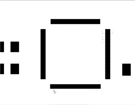
Clean Up the Outline & Get Cutting
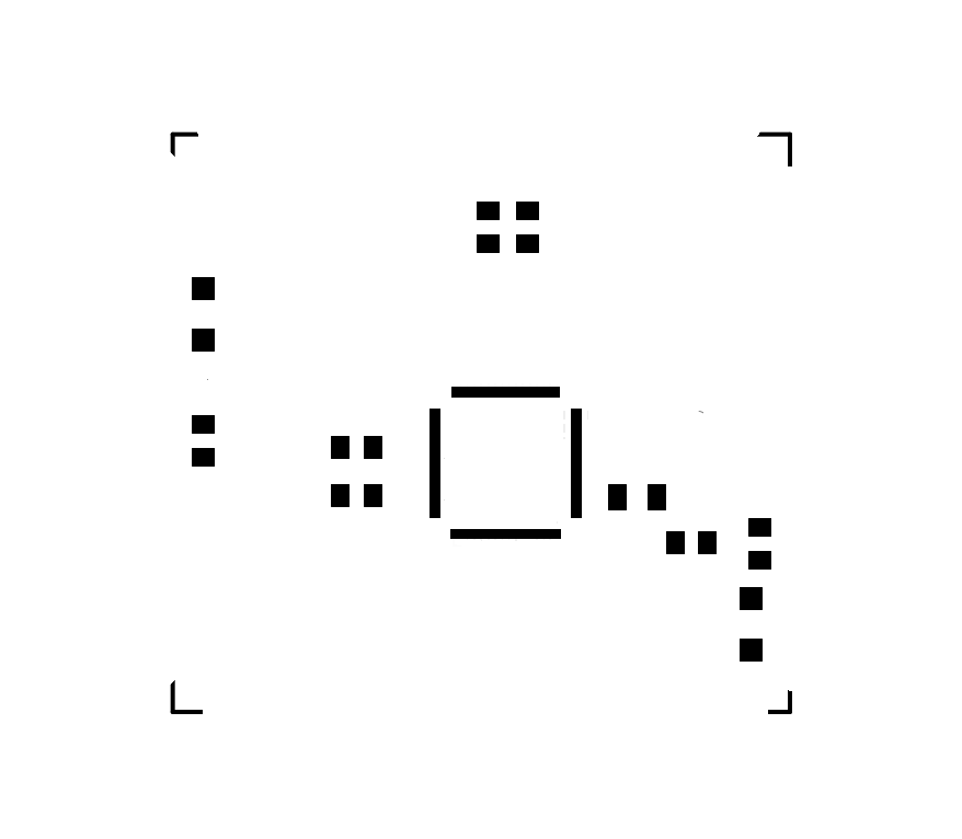
I like to remove most of the outside dimension line, but leave a little of each corner behind. This lets me measure the pattern when I print and it is a good reference for the board outline. You could cut out the pattern to the outside dimensions, but I like to leave a little extra area for when I tape down the pattern.
You can now print out the pattern on a sheet of coated paper and cut out the pattern with an X-acto knife. I found it works best to cut away from the center of each component pattern. Usually there is a blank section you need in the middle and you do not want to accidentally cut it off.
Optional Papercutter
If you happen to have a paper-cutting machine (these are popular with scrapbookers and other craft hobbyists) then you can export your file into a compatible format. The Silhouette Studio Designer software can convert svg or dxf (vector based format) files for use on the Silhouette machine.
I use this website to convert files to SVG format.
http://image.online-convert.com/convert-to-svg