LED Tower V2
.gif)
.gif)

Hey Everyone and what is up?
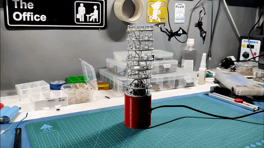
So this is the LED TOWER 2.0 which is basically a fancy Desk Lamp made by combining LEDs in a row and lighting them up individually to make a pattern.
8 LEDs are connecting in parallel on a Ring PCB that has a mosfet as a switch setup to drive the LEDs, we add 8 more Rings together in a row with jumper wires to make a tower-like setup that looks super cool when lighten up.
This Instructables is about the whole build process of this LED Tower, so let's get started.
Supplies
MATERIAL REQUIRED
- Custom PCBs x 8
- 5mm RED LEDs x 64
- 3D Printed Base
- AO3400 Mosfet
- 10K Resistor 0603
- 12 Ohms 1206
- Jumper wires
GETTING STARTED

This project is version 2 of my previous LED Tower project which was completely made by soldering LEDs together by jumper wires, LEDs were held in their place with a JIG and then soldered together by using their leads and jumper wires.
That project was made a few years ago, so to make V2 I planned to make a RING Shaped PCB that will hold LEDs in their place, These ring PCBs will be stacked up in a row by using leftover Leads of LEDs or we can use silver copper wire here as well.
SCHEMATIC
.jpg)
This is the schematic that was used in the project, all 8 LEDs are connected in parallel. an AO3400 Mosfet is connected with parallel LEDs with two Resistors in series with the LED.
R2 and R1 Resistors are connected in series with LEDs to limit the current of the LED when they are powered by VCC which will be around 5V.
The ring has one more Pad that is connected with a Resistor and then goes to the gate of mosfet, this pad is used to control the state of mosfet through a Microcontroller.
PWM Signal or HIGH LOW signal can be used to control the state of mosfet.
PCB DESIGN

here's the PCB Design that was made in such a way that it can be stacked up in a row by soldering jumper wires on its VCC and GND pads that are present on four parts of the PCB. On one side, Mosfet as a switch setup is placed along with 8 LEDs connected in parallel.
SEEED Fusion PCB Service
.gif)
.gif)
.gif)
After finalizing the PCB and generating its Gerber data, I send it to SEEED STUDIO for samples.
Ordered PCBs in white Soldermask with black silkscreen.
I received PCBs in a week and their quality was super good considering the rate which was also pretty low.
Seeed Fusion PCB Service offers one-stop prototyping for PCB manufacture and PCB assembly and as a result, they produce superior quality PCBs and Fast Turnkey PCBA within 7 working days.
PCB Quality of this Motor Controller PCB WAS SUPER!
Seeed Studio Fusion PCB Assembly Service takes care of the entire fabrication process from PCB manufacturing, parts sourcing, assembly, and testing services, so you can be sure that they are getting a quality product.
After gauging market interest and verifying a working prototype, Seeed Propagate Service can help you bring the product to market with professional guidance and a strong network of connections.
PCB ASSEMBLY
PCB Assembly of this project consists of four major steps which are
- Solder Paste Dispensing Process
- Pick & Place Process
- Hotplate Reflow
- Adding THT Components
SOLDER PASTE DISPENSING
.gif)

We start first by adding Solderpaste to each component pad on the bottom side of the board.
We do this process for all the Ring PCBs.
PICK AND PLACE
.gif)

Then we pick and place each component in its assigned place one by one.
We do this process for all 8 Ring PCBs.
HOTPLATE REFLOW
.gif)
.gif)
Next, we carefully lift all the PCBs and place them on the hotplate. I’m using my good old DIY hotplate which I made a while back.
Hotplate Heats the surface up to the solder paste melting temp and it slowly melts. after a few mins when the solder paste completely melts, we remove the PCB and let it cool down for a moment.
RESULT OF HOTPLATE PROCESS
.gif)
.gif)
Here's the PCB that has been reflow, Next we start the THT Process.
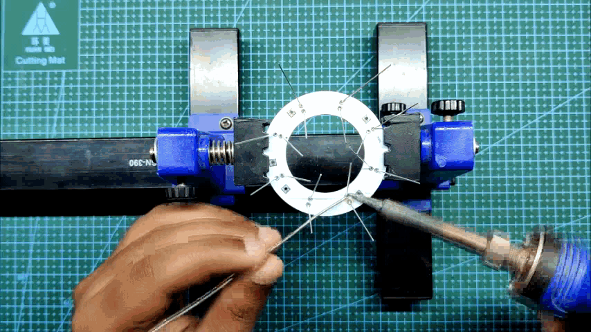
THT PROCESS
.gif)
.gif)
.gif)
.gif)
Here's the final setup, We add 5mm LEDs in their place one by one and then use a soldering iron to solder them in their place.
next, we use a wire cutter to remove the long LEGs of LEDs. (we will be using these LEGs to connect Rings in Row)
TESTING
.gif)
.gif)
.gif)
After soldering all the LED Ring PCBs completely, we move on to the next process which is to teach each LED Board, testing includes LED testing via a multimeter set in diode checking mode and MOSFET checkup by using an Arduino to control the gate of mosfet by providing it a PWM Signal.
We do both of the testings on each LED Ring PCB and move on to the next step which is the Assembly of the LED Tower.
FINAL ASSEMBLY 01
.gif)
.gif)
.gif)
.gif)
.gif)
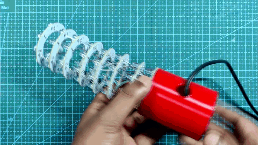
- We start the assembly of the LED Tower by first using a lead that was cut down from LED, we can also use silver copper wire here.
- We connect two LED Ring PCBs by soldering lead on one ring and soldering the other ring over it. Make sure to connect the lead in the right pad, the VCC lead will connect with the VCC lead of the other PCB, GND lead will be connected to the GND lead of the other PCB.
- We follow this same method and connect all 8 PCBs together in a row.
MAIN WIRING

.gif)
.gif)
.gif)
.gif)
- Next, we first add a few long wires to the signal pad of each LED Ring board along with two additional VCC and GND wires. VCC and GND of all Rings are already connected in parallel with leads.
- After this, we prepare a controller board by soldering two header pins for Arduino nano on a perf board.
- We then add all the signal wires with VCC and GND wires to the Arduino nano board by following the attached wiring diagram.
3D PRINTED BASE
.gif)
Here's the 3D Printed Base that I modeled to hold electronics inside and LED Ring Board outside, we mount the LED Ring on this Base by using Hotglue so no screw hole was added in the design.
The STEP file of this base is attached along with mesh files for the base and its lid.
FINAL ASSEMBLY 02
.gif)
.gif)
.gif)
.gif)
.gif)
- For final assembly, we first put the Arduino Nano in the 3D Printed Base and add hot glue to the base LED Ring PCB.
- Hot glue will attach the LED Ring Array to the 3D Printed base.
- We then connect a USB Cable to Arduino Nano and our setup is completed.
MAIN CODE
This is the main code that plays an animation by turning LED ROWs ON OFF that are connected to digital Pins of Arduino Nano.
int t = 40;
int rnd =5;
int pat1t =75;

void setup()
{
   for(int i=3; i<=12; i++)
   pinMode(i,OUTPUT);
}

void loop(){

   for(int i=0; i<=rnd; i++) {
   pat1();}
   for(int i=0; i<=rnd; i++){
   pat2();}
   for(int i=0; i<=rnd; i++) {
   pat3();}
   for(int i=0; i<=rnd; i++) {
   pat4();}
   for(int i=0; i<=rnd; i++){
   pat5();}
   for(int i=0; i<=rnd; i++) {
   pat6();}
   for(int i=0; i<=rnd; i++) {
   pat7();}
   for(int i=0; i<=rnd; i++) {
   pat8();}
   for(int i=0; i<=rnd; i++) {
   pat9();}


}

void pat1(){
    for(int i=3; i<=12; i++) {
      digitalWrite(i,HIGH);
      delay(pat1t);
      digitalWrite(i,LOW);

    }

    for(int i=11; i>=4; i--) {
      digitalWrite(i,HIGH);
      delay(pat1t);
      digitalWrite(i,LOW);
    }
}
void pat2(){
     for(int i=3; i<=12; i++) {
      digitalWrite(i,HIGH);
      digitalWrite(i-1,HIGH);
      digitalWrite(i+1,HIGH);
      delay(100);
      digitalWrite(i,LOW);
      digitalWrite(i-1,LOW);
      digitalWrite(i+1,LOW);
    }

    for(int i=11; i>=4; i--) {
      digitalWrite(i,HIGH);
      digitalWrite(i-1,HIGH);
      digitalWrite(i+1,HIGH);
      delay(100);
      digitalWrite(i,LOW);
      digitalWrite(i-1,LOW);
      digitalWrite(i+1,LOW);
    }
}
void pat3(){
  for(int i=3; i<=12; i=i+2) {
      digitalWrite(i,HIGH);
      delay(100);
      digitalWrite(i,LOW);

    }

    for(int i=12; i>=3; i=i-2) {
      digitalWrite(i,HIGH);
      delay(100);
      digitalWrite(i,LOW);
    }
}
void pat4(){
      for(int i=3; i<=12; i++) {
      digitalWrite(i,HIGH);
      delay(100);
    }

    for(int i=12; i>=2; i--) {
      digitalWrite(i,HIGH);
      delay(100);
      digitalWrite(i,LOW);
    }
}
void pat5(){
     for(int i=3; i<=12; i++) {
      digitalWrite(i,HIGH);
      }
    delay(100);
    for(int i=3; i<=12; i++) {
      digitalWrite(i,LOW);
      }
    delay(100);
}
void pat6(){
       for(int i=3; i<=8; i++) {
      digitalWrite(i,HIGH);
      }
    for(int i=8; i<=12; i++) {
      digitalWrite(i,LOW);
      }
    delay(200);
    for(int i=3; i<=8; i++) {
      digitalWrite(i,LOW);
      }
    for(int i=8; i<=12; i++) {
      digitalWrite(i,HIGH);
      }
    delay(200);
}
void pat7(){
       for(int i=3; i<=12; i=i+2) {
      digitalWrite(i,HIGH);
      }
    for(int i=4; i<=12; i=i+2) {
      digitalWrite(i,LOW);
      }
    delay(200);
     for(int i=3; i<=12; i=i+2) {
      digitalWrite(i,LOW);
      }
    for(int i=4; i<=12; i=i+2) {
      digitalWrite(i,HIGH);
      }
    delay(200);
}
void pat8(){
    digitalWrite(7,HIGH);
    digitalWrite(8,HIGH);
    delay(t);
    digitalWrite(7,LOW);
    digitalWrite(8,LOW);
    delay(t);
    digitalWrite(6,HIGH);
    digitalWrite(9,HIGH);
    delay(t);
    digitalWrite(6,LOW);
    digitalWrite(9,LOW);
    delay(t);
    digitalWrite(5,HIGH);
    digitalWrite(10,HIGH);
    delay(t);
    digitalWrite(5,LOW);
    digitalWrite(10,LOW);
    delay(t);
    digitalWrite(4,HIGH);
    digitalWrite(11,HIGH);
    delay(t);
    digitalWrite(4,LOW);
    digitalWrite(11,LOW);
    delay(t);
    digitalWrite(3,HIGH);
    digitalWrite(12,HIGH);
    delay(t);
    digitalWrite(3,LOW);
    digitalWrite(12,LOW);
    delay(t);
     digitalWrite(4,HIGH);
    digitalWrite(11,HIGH);
    delay(t);
    digitalWrite(4,LOW);
    digitalWrite(11,LOW);
    delay(t);
    digitalWrite(5,HIGH);
    digitalWrite(10,HIGH);
    delay(t);
    digitalWrite(5,LOW);
    digitalWrite(10,LOW);
    delay(t);
    digitalWrite(6,HIGH);
    digitalWrite(9,HIGH);
    delay(t);
    digitalWrite(6,LOW);
    digitalWrite(9,LOW);
    delay(t);
}

void pat9(){
    for(int i=3; i<=12; i++) {
      digitalWrite(i,HIGH);
    }
     for(int i=3; i<=12; i++) {
      digitalWrite(i,LOW);
      delay(100);
      digitalWrite(i,HIGH);
    }
    for(int i=11; i>=4; i--) {
      digitalWrite(i,LOW);
      delay(100);
      digitalWrite(i,HIGH);
    }

}
RESULT
.gif)
.gif)
Here's the result and as you can see, LED Tower is working.
For power, we can use any 5V Source like a power bank or smartphone adaptor.
This LED Tower is like a dumb version of LED Cube, it works with one row but the cube has multiple rows so maybe we can prepare a similar setup by using more leds and digital I/O Ports for Version 3.
Stay tuned for the next project, all the Docs related to the project are attached, if you need any help regarding this project, DM me or comment.
Special thanks to Seeed Studio for providing PCBs for this project, do check them out if you need great PCB Service for less cost.
Peace out and I'll be back with a new project soon!