KiCAD Basic Tools
.gif)
KiCad
KiCad is an open-source software tool for the creation of electronic schematic diagrams and PCB artwork.[1]
KiCad includes a set of main software tools [1]:
- KiCad: The project manager
- Eeschema: Schematic editor and component editor
- Pcbnew : Circuit board layout editor and footprint editor (PCB layout program). It also has a 3D view.
- Gerbview : the Gerber viewer
- Bitmap2component : A tool to convert images to footprints for PCB artwork.
Eeschema Basic Tools
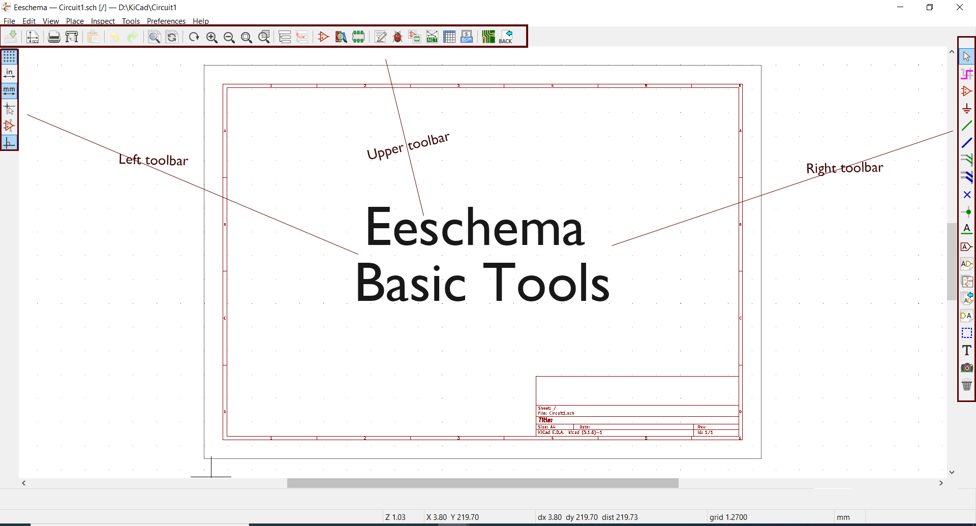.gif)
Upper Toolbar Tools
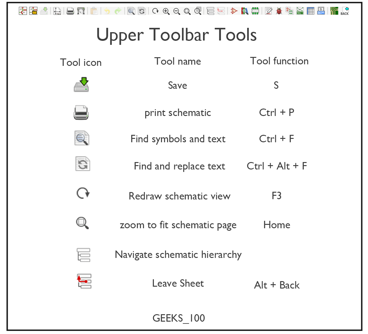
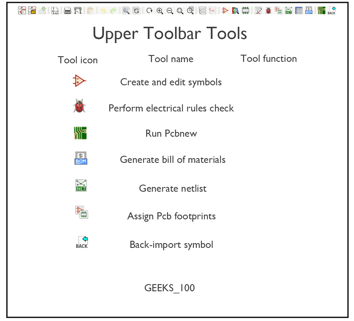
Some of Upper Toolbar Tools:[2]
Save Tool: Save complete schematic project.
print schematic Tool: Open print dialog.
Find symbols and text: Show the dialog to search symbols and texts in the schematic.
Find and replace text: Show the dialog to search and replace texts in the schematic.
Redraw schematic view: Refresh screen.
zoom to fit : zoom to fit schematic page.
Navigate schematic hierarchy: View and navigate the hierarchy tree.
Leave Sheet: Leave the current sheet and go up in the hierarchy.
Create, delete and edit symbols: Call the symbol library editor to view and modify libraries and symbols.
Perform electrical rules check: Electrical Rules Checker (ERC), automatically validate electrical connections.
Run Pcbnew to layout printed circuit board: Call Pcbnew to perform a PCB layout.
Generate bill of materials: Generate the Bill of Materials (BOM).
Generate netlist: Export a netlist (Pcbnew, SPICE and other formats).
Assign PCB footprints to schematic symbols: Call CvPcb to assign footprints to symbols.
Back-import: Back-import footprint assignment (selected using CvPcb or Pcbnew) into the "footprint" fields.
Right Toolbar Tools
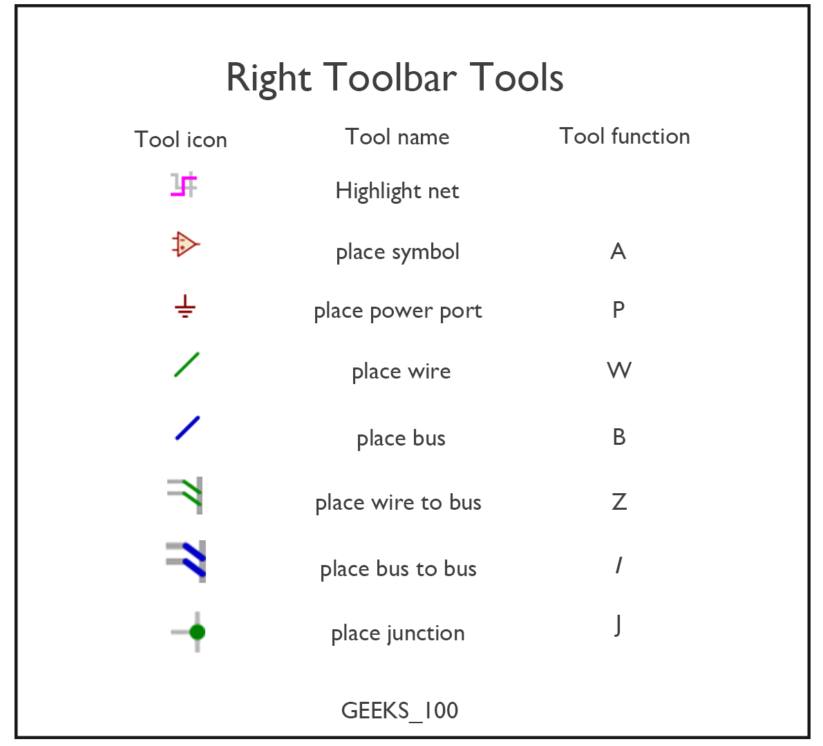
Some of Right Toolbar Tools:[2]
Highlight net: Highlight a net by marking its wires and net labels with a different color. If KiCad runs in project mode then copper corresponding to the selected net will be highlighted in Pcbnew as well.
place symbol: Display the symbol selector dialog to select a new symbol to be placed.
place power port: Display the power symbol selector dialog to select a power symbol to be placed.
place wire: Draw a wire.
place bus: Draw a bus.
place wire to bus: Draw wire-to-bus entry points. These elements are only graphical and do not create a connection, thus they should not be used to connect wires together.
place bus to bus: Draw bus-to-bus entry points.
place junction: Place a junction. This connects two crossing wires or a wire and a pin, when it can be ambiguous (i.e. if a wire end or a pin is not directly connected to another wire end).
Left Toolbar Tools
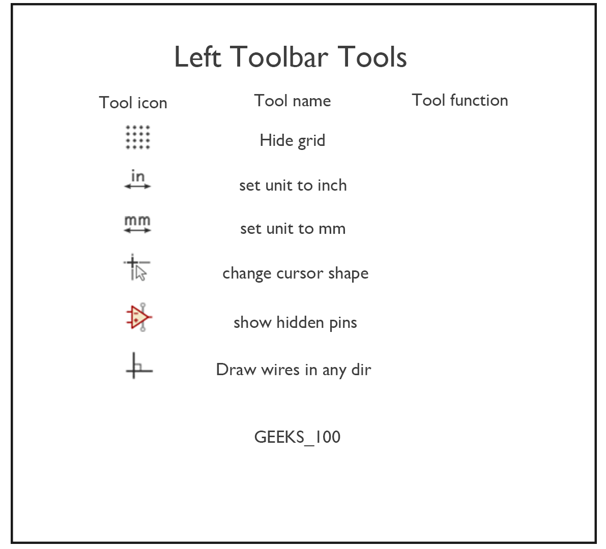
Left Toolbar Tools:[2]
Hide grid: Toggle grid visibility.
set unit to inch: Switch units to inches.
set unit to mm: Switch units to millimeters.
change cursor shape: Choose the cursor shape (full screen/small).
show hidden pins: Toggle visibility of "invisible" pins.
Draw wires and buses in any direction: Toggle free angle/90 degrees wires and buses placement.
Thanks for reading.