Just a Regular OverEngineered FlowerPot
by Arnov Sharma in Circuits > Art
1416 Views, 6 Favorites, 0 Comments
Just a Regular OverEngineered FlowerPot


So Here's something Super Cool and unique, A Flower Pot made completely out of PCBs.
I made this flowerpot by combining three different PCBs, I used a diamond-shaped board as a flower petal by soldering them together in star-shaped form.
This project is a combination of electronics and art by pushing the limits of how and where we can use PCBs in so many different things.
This Instructables is gonna be about the build Process of the whole Flower so let's get started.
Supplies
These were the things I used in this build-
- Custom PCBs (Base PCB, Diamond-shaped PCB, STEM PCBs, and Tear Shaped PCB)
- Atmega328PU
- IP5306 Power Management IC
- 10uF Capacitor 0805 Package
- Resistor 10K 0603 Package
- Resistor 1K 0603 Package
- Resistor 3R3
- 1H Inductor
- Push Button SMD
- Push Button THT
- ON-OFF Switch
- Type C Port
- 22pf Capacitor
- Indicator LED 0603 Package
- 8205S Mosfets
- Connecting Wires
- WHITE LEDs 0603 Package
- BLUE LEDs 0603 Package
- 3D Printed PCB HOLDERs
- 3D Printed Vase
- Lithium-Ion cell 18650 Holder
- Lithium-Ion cell 3.7V 2200mah Cell
Prologue
.gif)
.gif)
.gif)

I used a previously made PCB as a leaf because its shape was somewhat similar to an actual leaf.
As for the stem, I prepared a PCB that holds the flower and leaf together, this stem is then soldered on a base that holds the whole structure and also contains the control board.
I've added LEDs on Petals and Leaf, these LEDs connected are in parallel. LEDs on each PCB are connected in parallel, they are all driven by six MOSFETs that are on the Base PCB.
These Mosfets are controlled by an Atmega328PU, we can turn them ON-OFF in sequence or dim them down or do some fading effects on them.
As for the Power, I've added a Boost IC Setup on the base that boosts 3.7V from the Lithium Cell into 5V for powering the LEDs and Microcontroller.
Basic Concept
.gif)

.gif)
This idea came into existence almost two weeks ago, I prepared a diamond-shaped PCB necklace, and after finishing the project I noticed that it could be aligned side by side in a polygon shape, a pentagram to be specific.
So I taped five diamond-shaped PCBs together and made a PCB Flower just to visualize the idea.
As for the rest, I prepared a rectangular board that is long and have three big holes for connecting two or more PCBs.
For Leaf, I used a PCB from my previous project as the PCB Shape was similar to an actual leaf.
For Driving LEDs, Six N Channel Mosfet ICs were used which are connected to six PWM Pins of Atmega328PU.
SCHEMATIC for the Main Controller Board
.jpg)
The Controller board consists of three main sections, the Atmega328PU Setup, Boost Module part, and Mosfet setup.
I used Atmega328PU here instead of using an MCU like Arduino as I wanted to make this project from scratch instead of using modules and addons.
The whole setup is powered by IP5306 IC that takes 3.7V from lithium-Ion Cell and boosts it up to 5V for driving MCU and LEDs.
PCB DESIGN of Main Board

After finalizing the schematic, I prepare the PCB Design of the base board by using a 100mm Circle as an outline and putting all the components inside this circle.
I've added a Slot in the middle of the PCB, This slot will hold the STEM PCB, I also added all the MOSFETs setup around this slot so it would be easy to connect the LED section with each of its MOSFETs through connecting wires.
PCB DESIGN of STEM Board


For Stem Board, I added three CON1 and connected them with each other.
As for the PCB Design, I used a Mechanical Hole Pad of hole size 5mm in each CON1 so it would be easier to attach two or more by using nuts and bolts or solder them other as these holes will be plated from inside and outside.
Getting PCBs From PCBWAY
.gif)
.gif)
.gif)

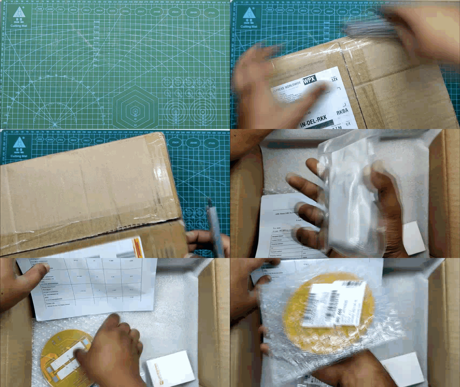
After finalizing both of the designs, I exported their Gerber data and upload it on PCBWAY's quote page.
I Choose a Yellow soldermask with white silkscreen for the Base Board and Green Soldermask for STEM Board.
I received PCBs after a week which was super fast. As for the PCB Quality, it was super good.
You guys can check PCBWAY out if you need great PCB Service for High-Quality stuff at an affordable rate.
Just see the intricate design of mine, I placed many unusual patterns on the PCB like irregular outlines and shapes of soldermask which is hard to make but they did an awesome job of making the PCBs with no problem whatsoever.
Checkout PCBWAY from here- https://www.pcbway.com/
Base Controller Board Assembly
.gif)
.gif)
.gif)
.gif)
.gif)
.gif)
- I first started the Base board assembly process. first, we add solder paste to each component pad one by one with a solder paste dispenser.
- We then gather all the components and place them in their place.
- Next, we add the PCB on an SMT Hotplate that heats up the PCB from Below up to the solder paste melting temperature.
- Later, I added SMD Lithium Ion cell Holder on the bottom side
Base Controller Board Testing
.gif)
.gif)
.gif)
The next step is to test the Boost module setup, so I added a Lithium Cell to its SMD holder and turn ON the setup by using the SMD Switch on the board.
This triggers the IP5306 IC and its indication LEDs glow up indicating the battery percentage.
We measure the output voltage of this setup by using a multimeter, the output voltage was 5V which indicates this part of the base board is working properly.
Next, we add a Type C Charger to this setup in order to check if the indication feature is working or not.
IP5306 has four LED-based indication feature that shows the battery percentage of 25% 50% 75% and 100%.
After testing the Power management setup properly, we move on to the next step which is to add THT Components to the base board.
Adding THT Components
.gif)
.gif)
.gif)
Next, I gather all the THT components and started the THT Assembly by placing them in their right place and then soldering their pads using a Regular soldering Iron.
Leaf PCB Assembly
.gif)
.gif)
.gif)
For the Leaf PCB Assembly, we first gather 24 White 0603 LEDs and start by adding solder paste to the LED Pads on the PCB.
Next, we Pick and place each LED and then use the SMT Hotplate to melt the solder paste.
Petal PCB Assembly
.gif)
.gif)
.gif)
.gif)
.gif)
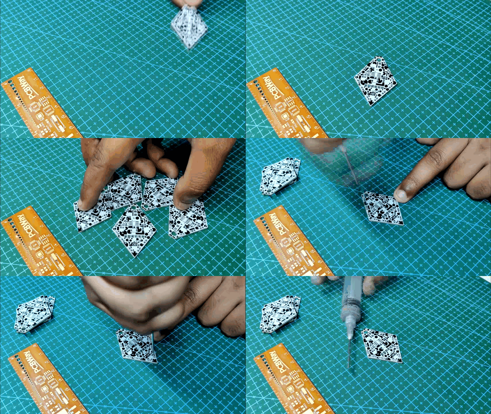
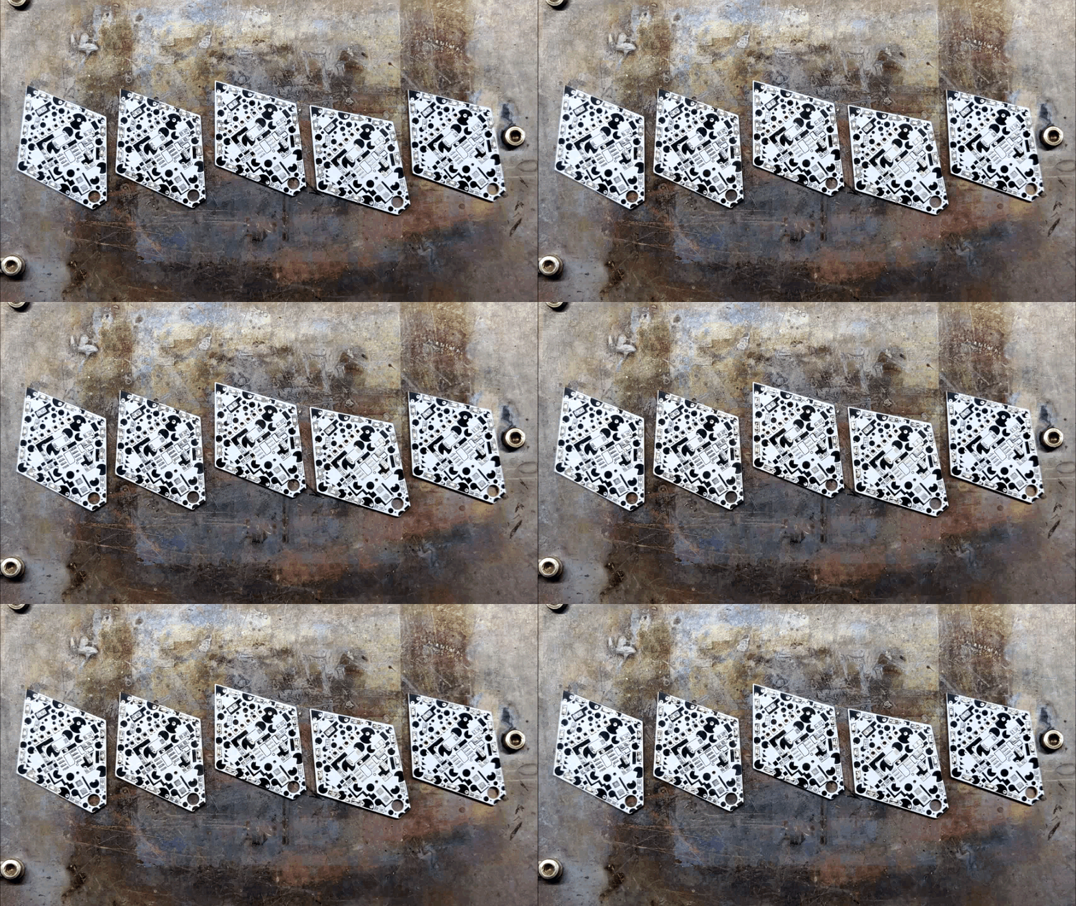
For Petal PCB Assembly, I used 12 Blue LEDs of 0603 Package and start the assembly by first applying solder paste to LED Pads on the PCB.
We then pick and place each LED in its assigned place and put the whole board on SMT Hotplate for reflow.
Because we are preparing a Pentagon Flower, we need to prepare a total of five boards.
Editing Part in Petal and Leaf PCB
.gif)

Next, We connect all the LEDs in parallel by using a few jumper wires to connect their negative together as in the previous board, six LEDs were connected in parallel and they were driven by a single mosfet and I've used four Mosfets to control four sections of LEDs so its important to connect all LEDs in Parallel by connecting their negative terminal together.
We do this process in both Petal and Leaf boards and then move on to the next process which is to test each board's LED continuity.
Testing Leaf and Petal PCBs
.gif)
.gif)
Next, We use a multimeter set in diode checking mode to check the LEDs by connecting the positive probe of the multimeter on the Positive terminal of the LED and the negative probe to the negative terminal.
We check both Leaf and all Petal PCBs with the same method.
FLOWER ASSEMBLY

.gif)
.gif)
The first step is to gather all the Diamond-shaped PCBs and add tape on the back side to hold two PCBs together.
By following this method, we attach five PCBs together in a pentagon shape.
Next, we add super glue in between all the PCBs so they fuse together and make one single flower-like structure.
Preparing STEM
.gif)
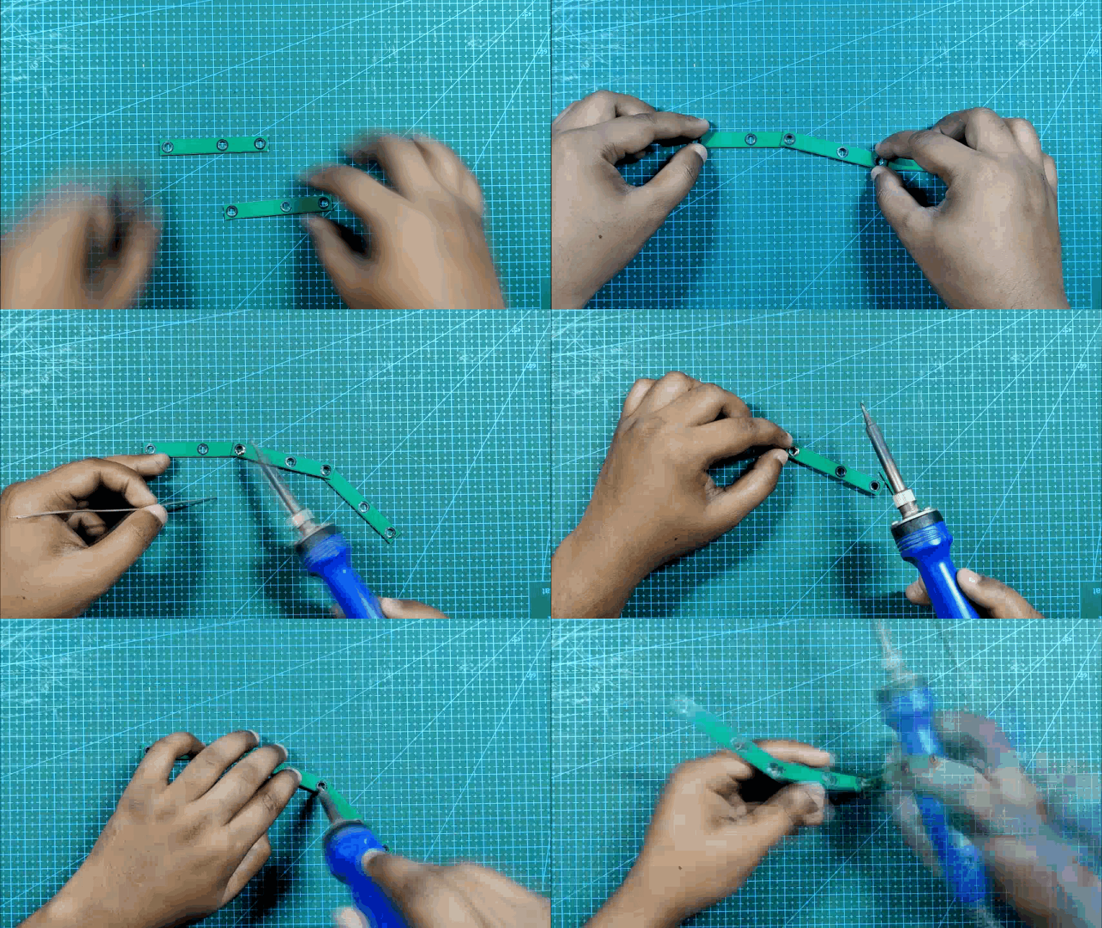
We then prepare the STEM part by soldering three STEM PCBs together in a curve pattern, kinda like an Arc made from three lines.
LEAF and STEM ASSEMBLY
.gif)
.gif)
.gif)
Next, we connect Leaf PCB with STEM Structure by using a 3D Printed Circuit holder that we screw to STEM PCB first and then add Leaf PCB on it.
FLOWER and STEM ASSEMBLY
.gif)
Similarly, we add Flower Structure with the Leaf and STEM assembly by using another 3D Printed Circuit holder that connects STEM with Flower.
MAIN ASSEMBLY
.gif)
.gif)
.gif)
.gif)
Next is the main assembly in which we start first by connecting the upper flower with the base by putting the STEM PCB in the slot on the base PCB, we then solder the pads of STEM PCB with Base pads and this secures the PCB in its place.
WIRING
.gif)
.gif)
.gif)
.gif)
.gif)
.gif)
The last process of this build is to wire everything up.
We start first by connecting the positives of all the LEDs that are being used in the flower portion and the leaf together.
Then we connect wires from the negative of each LED Section to a mosfet Switch present on the base PCB.
There are a total of 6 different LED Sections, five petals, and one leaf. Six MOSFETs control each section and their VCC are common. GND of each LED section goes into Mosfet's Drain port.
CODE and Flashing the Atmega328PU
.gif)
Because I'm using an Atmega328PU MCU, we cannot directly connect it with a USB and put code into it.
In order to flash code in it, we first need to burn the bootloader by using an ISP Device that connects the SPI Pins of the MCU with its ISP pins and lets us flash the MCU.
I used my previously made Arduino as ISP Module which is an easy-to-make setup for flashing AVR MCUs.
We connect the Base Module's ISP Pins with SPI Pins of Arduino setup by following this wiring layout.
- VCC to VCC
- GND to GND
- D13 of Arduino to D13 of Atmega328PU
- D12 of Arduino to D12 of Atmega328PU
- D11 of Arduino to D11 of Atmega328PU
- D10 of Arduino to RESET PIN of Atmega328PU
As for the code, I first used the test sketch which was a chase sketch that turns ON and OFF LEDs in a chaser sequence. This sketch was just for testing.
int pinsCount=6;                        // declaring the integer variable pinsCount
int pins[] = {3,5,6,9,10,11};          // declaring the array pins[]


void setup() {
  pinMode(3, OUTPUT);
  pinMode(5, OUTPUT);
  pinMode(6, OUTPUT);
  pinMode(9, OUTPUT);
  pinMode(10, OUTPUT);
  pinMode(11, OUTPUT);


}


void loop() {
  for (int i=0; i<pinsCount; i=i+1){    // chasing right
    digitalWrite(pins[i], HIGH);         // switching the LED at index i on
    delay(70);                          // stopping the program for 100 milliseconds
    digitalWrite(pins[i], LOW);          // switching the LED at index i off
  }
  for (int i=pinsCount-1; i>0; i=i-1){   // chasing left (except the outer leds)
    digitalWrite(pins[i], HIGH);         // switching the LED at index i on
    delay(70);                          // stopping the program for 100 milliseconds
    digitalWrite(pins[i], LOW);          // switching the LED at index i off
  }

}
Here's the final sketch that I used in this project.
const int switchPin = 2;
int pinsCount=5;                        // declaring the integer variable pinsCount
int pins[] = {3,5,6,9,10};
int lightMode = 1;

int led = 11;           // the PWM pin the LED is attached to
int brightness = 0;    // how bright the LED is
int fadeAmount = 5;    // how many points to fade the LED by

void setup()
{
  pinMode(3, OUTPUT);
  pinMode(5, OUTPUT);
  pinMode(6, OUTPUT);
  pinMode(9, OUTPUT);
  pinMode(10, OUTPUT);
  pinMode(switchPin, INPUT_PULLUP);
  pinMode(led, OUTPUT);
  digitalWrite(3, LOW);
  digitalWrite(5, LOW);
  digitalWrite(6, LOW);
  digitalWrite(9, LOW);
  digitalWrite(10, LOW);

}
void loop()
{
    if (digitalRead(switchPin) ==LOW)
    {
        lightMode = lightMode + 1;
        if (lightMode == 3)
        {
            lightMode = 1;
        }
    }
    if (lightMode == 1)
    {
        digitalWrite(pins[3,5,6,9,10], LOW);
        delay(1000);
    }
    else if (lightMode == 2)
    {
      for (int i=0; i<pinsCount; i=i+1){    // chasing right
      digitalWrite(pins[i], HIGH);         // switching the LED at index i on
      delay(70);                          // stopping the program for 100 milliseconds
      digitalWrite(pins[i], LOW);          // switching the LED at index i off
    }
      for (int i=pinsCount-1; i>0; i=i-1){   // chasing left (except the outer leds)
      digitalWrite(pins[i], HIGH);         // switching the LED at index i on
      delay(70);                          // stopping the program for 100 milliseconds
      digitalWrite(pins[i], LOW);          // switching the LED at index i off
     }
    }
       analogWrite(led, brightness);
       brightness = brightness + fadeAmount;
       if (brightness <= 0 || brightness >= 255) {
    fadeAmount = -fadeAmount;
  }
  delay(30);
    //delay(200); // see text
}
RESULT


Here's the result of this crazy-built, OverEngineered Flower Pot that is made completely from PCBs.
We first turn ON the ON-OFF Switch that turns ON the IP5306 IC and it powers the atmega328PU MCU.
To start the LED Sequence, we use the toggle switch to start or stop the LED Animations.
This is it for today folks, stay tuned and I'll be back with a new project soon.
Special thanks to PCBWAY for supporting this project, Check them out for getting great PCB Service for less cost.
Peace