How to Design a Maker-type PCB Stack in Eagle
by ahmetakman in Circuits > Electronics
247 Views, 1 Favorites, 0 Comments
How to Design a Maker-type PCB Stack in Eagle
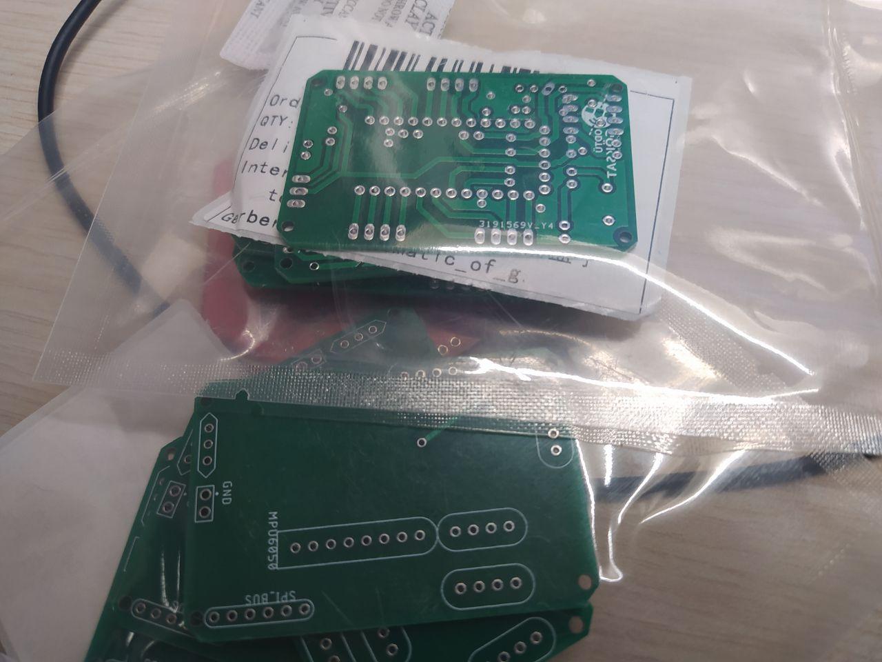
In this text, we would provide necessary instructions for designing PCB stacks in a simple sense. After designing your PCB stack, you can easily materialize your designs using JLCPCB's super-simple interface. Thanks to JLCPCB, our precious readers and dear makers can acquire high quality PCBs and pay less than others.
Makers generally do not prefer designing PCBs by a modular approach. But in iterative design processes, in which designers gradually change their designs during the prototyping phase, it could lower the price and benefit the maker by avoiding the manufacturing of the whole PCB multiple times.
Now, Let's dive in and explain how you can design your own PCB stack.
Supplies
https://jlcpcb.com
Drawing a Schematic
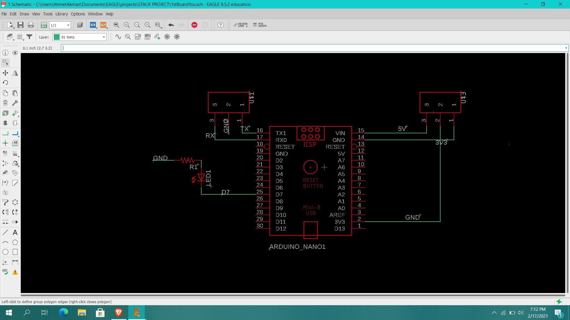
Initial step for designing a PCB is making a schematic of the electrical components and their connections. Designing a modular PCB stack is no different. Firstly, you should open a new schematic file in your PCB designing software. Autodesk Eagle is the preffered software for this text. After you've done that, you should add your components. Most softwares only allow you to add them one by one. Then, you should connect your components with wiring tool. Then, you should name your connections for readability. This would allow our software to create connections automaticly when we turn this schematic into a PCB.
Completing Your Board Design
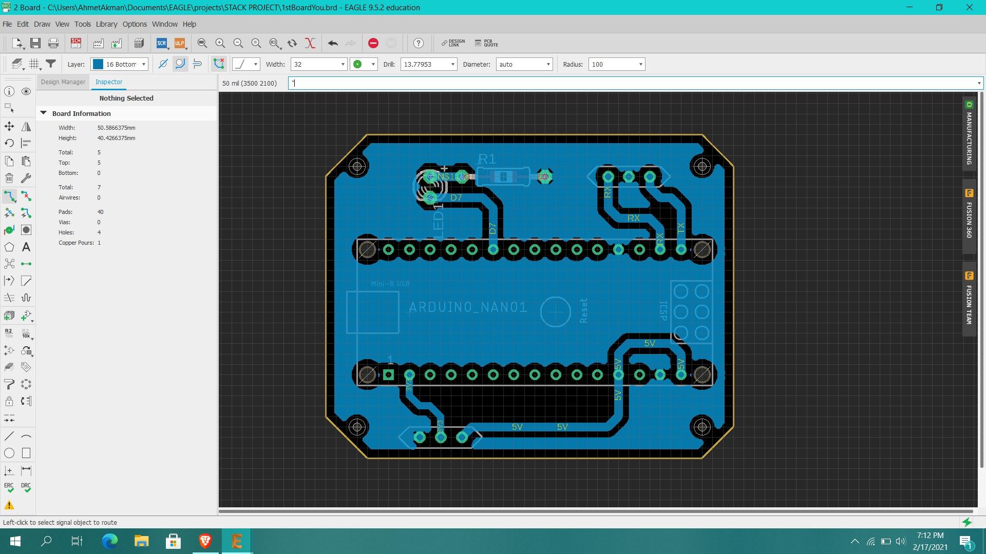
After completing your schematic design, click "Switch to Board" button on Eagle interface. This would automatically transform your schematic design into a PCB design. During this phase, you can reorganize the wirings and make your PCB simpler and easier to produce. But thanks to JLCPCB, there is no need to do that because there is no PCB they cannot produce. After this phase, Our PCB's skeleton is ready.
Exporting Your PCB Design As DXF
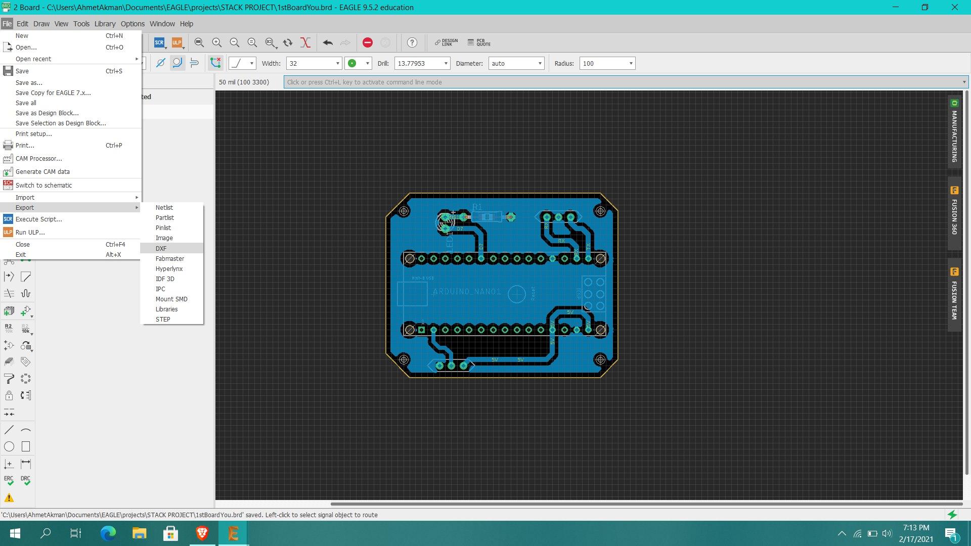
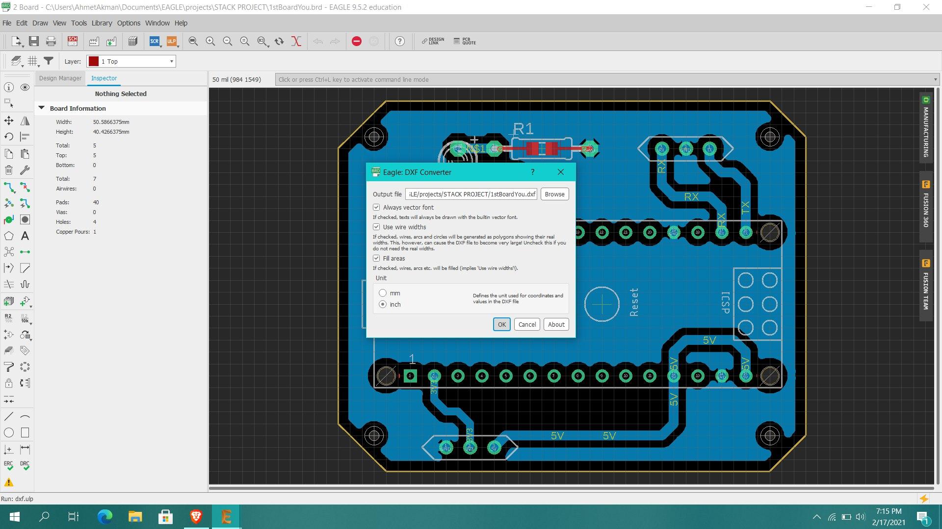
DXF format is used for creating a template of our PCB. This allows us to create multiple layers of PCBs with same fundamental holes; Therefore, we will be able to create a pcb stack with those layers.
Importing DXF and Designing PCB Layers
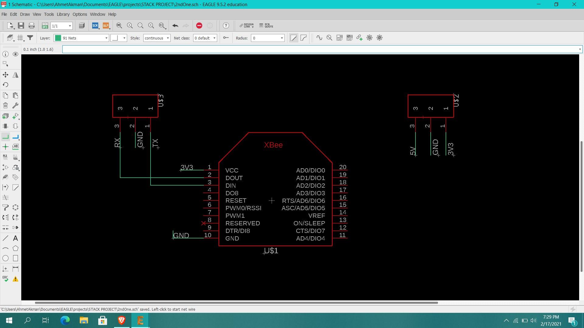
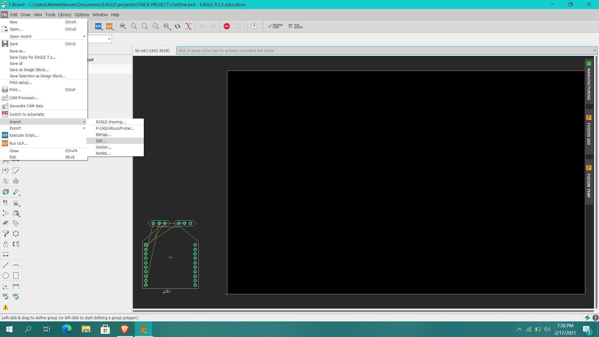
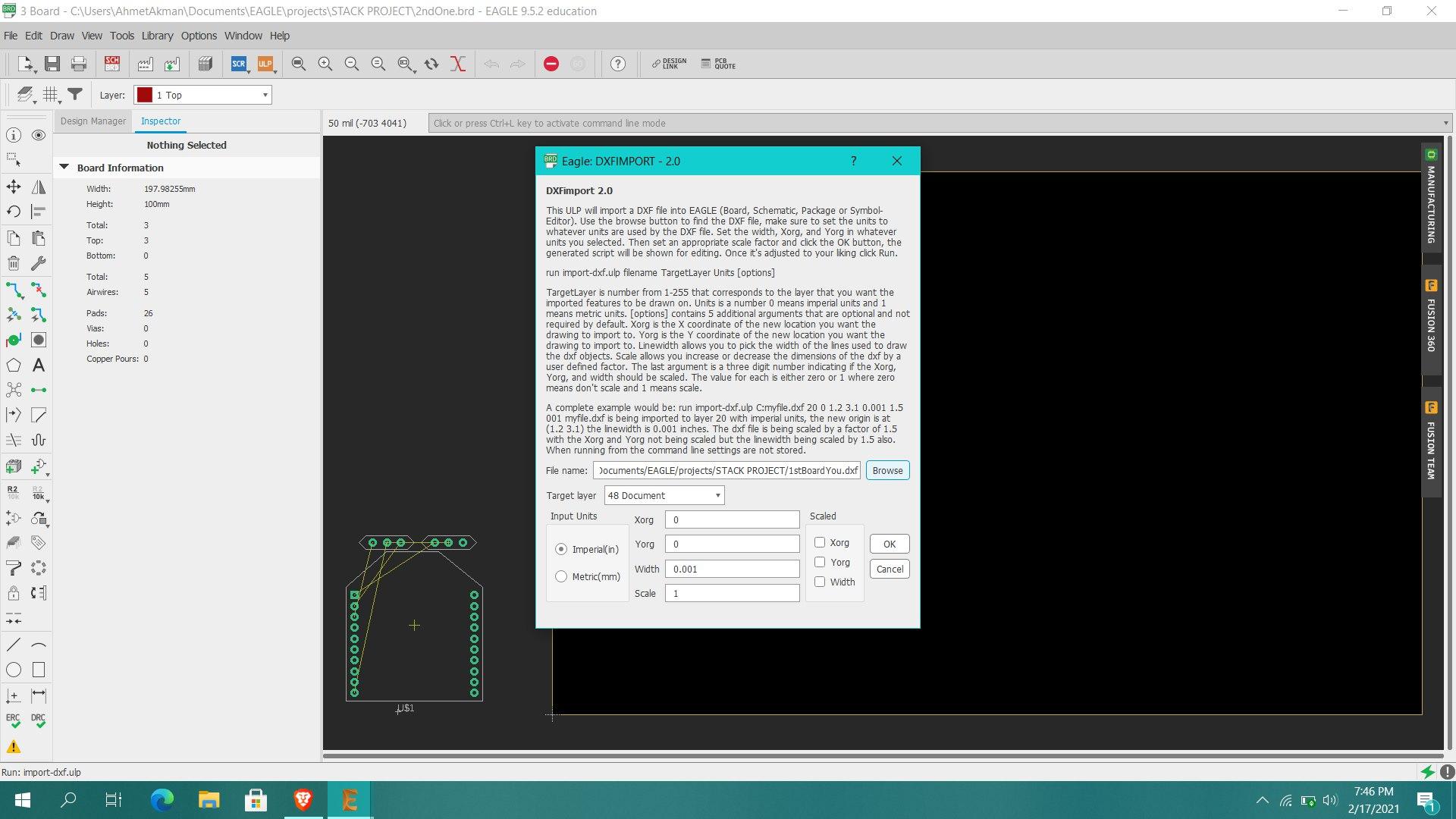
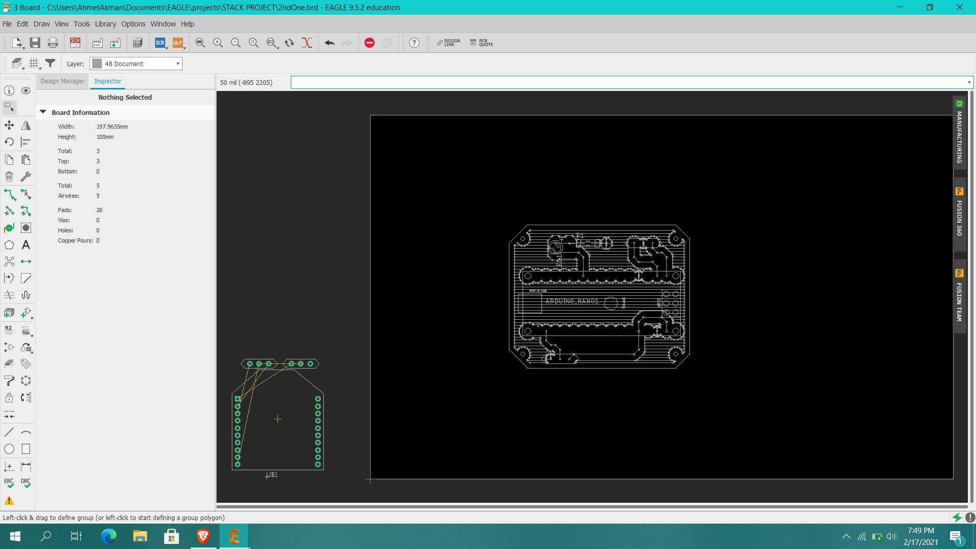
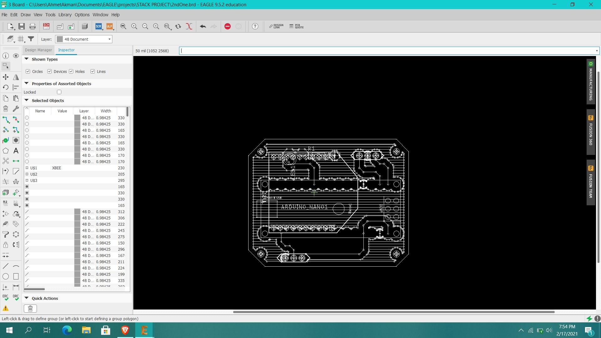
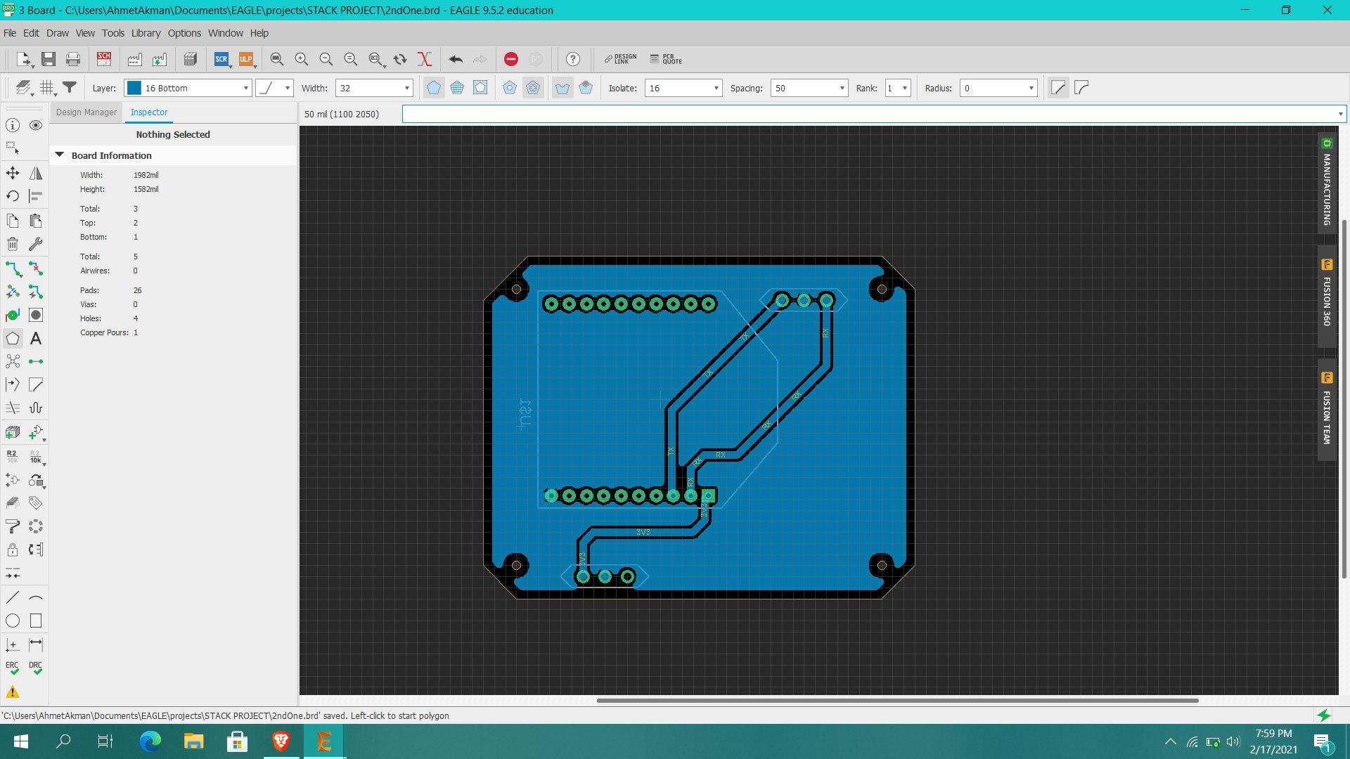
After exporting your fundamental design as DXF, we should import it in order to use it as a template . Then, we will create our layers from schematic step using that template, so we would easily recognize the mutual connections and create a completely compatible PCB stack. Now, our pcb stack is as good as ready.
Why Should You Choose to Design Modular PCBs
Modular designs are always a life saver if you encounter an error during your project. You could immediately find which board is causing that error and your whole design does not get affected by that error. A simple change in the design of that particular board would be enough to save your project and it would be significantly cheaper than changing the whole design. If you are working on a project that has multiple objectives, that flexibility on your design not only would let you focus on the problems part by part, but also make the problems simpler by dividing them into multiple parts.
Manufacturing Your PCBs
After doing a great job on design, We believe that your PCB design deserves the best. You can send your beautiful PCB designs to JLCPCB for the best feasable manufacturing option available on our planet.