How to Convert Your Circuit Idea Into Printed Circuit Board (PCB)
by MissionCritical in Circuits > Electronics
19158 Views, 53 Favorites, 0 Comments
How to Convert Your Circuit Idea Into Printed Circuit Board (PCB)
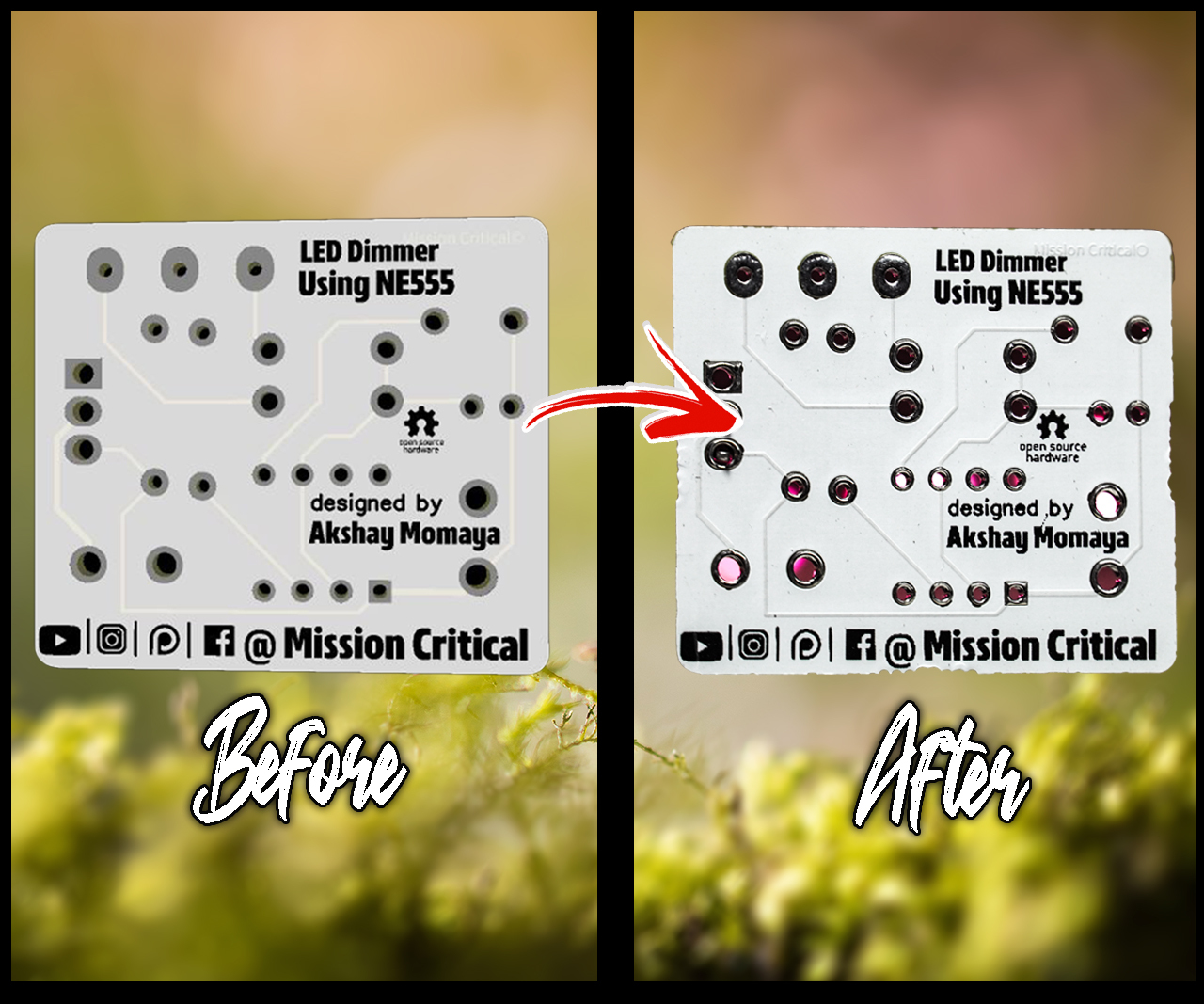
In this tutorial, we will learn the entire process of PCB Designing that is Printed Circuit Board, we will learn how to convert our electronic circuit Idea into a reality using EASYEDA and an online PCB manufacturing service.
so follow up till the end to convert your idea from circuit to reality.
Supplies
1. Hardware
- Computer.
- Soldering Iron.
- Soldering Wire.
- Helping Hands.
- Solder Fume Extractor.
- Wire Stripper.
- 12v power supply.
2. Software
3. Components
Watch the Video
Idea
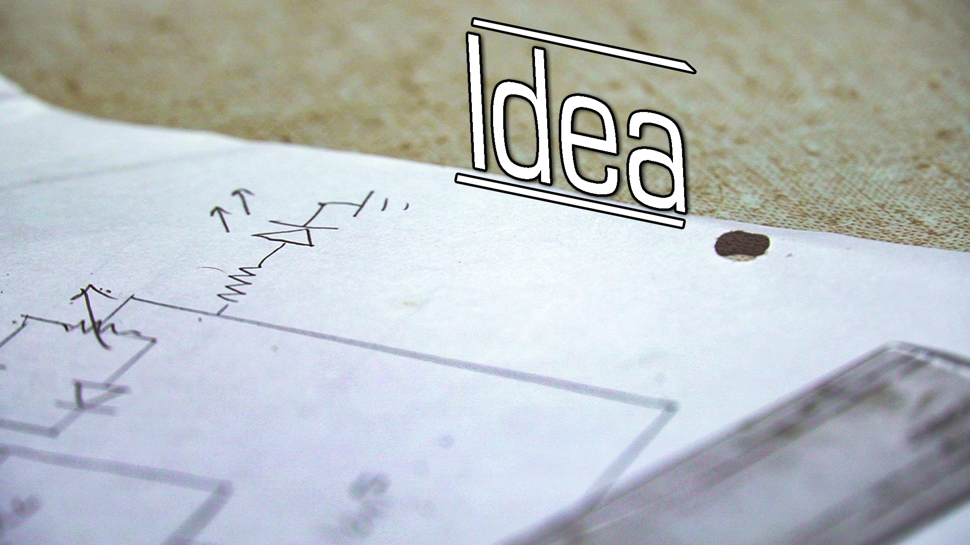
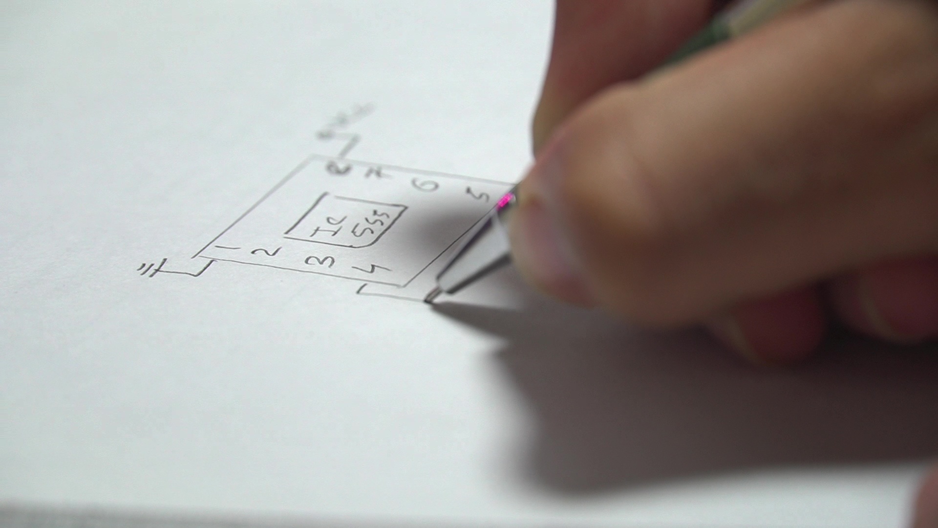
First step for any electronic project is IDEA, so for today’s tutorial, let’s make something simple, something easy to build and understand, for which we will make a LED dimmer circuit based on ic NE555.
IC555 is capable of generating PWM signal which can control the amount of power delivered to the given LED. Pulse Width Modulation (PWM) is a fancy term for describing a type of digital signal. When the signal is high, we call this “on time”. To describe the amount of “on time”, we use the concept of the duty cycle.
If the percentage of duty cycle is higher than 50%, the digital signal spends more time in the high state than the low state and vice versa if the duty cycle is less than 50%. Here graph that illustrates
Four scenarios: 100% Duty Cycle= avg 5V
75% Duty Cycle= avg 3.75V
50% Duty Cycle= avg 2.5V
25% Duty Cycle= avg 1.25
thus making the intensity of LED low and overall works as a LED dimmer.
So now that we have an idea, let’s draw it out on paper.
( schematic can be found here for reference )
Test Circuit on Breadboard
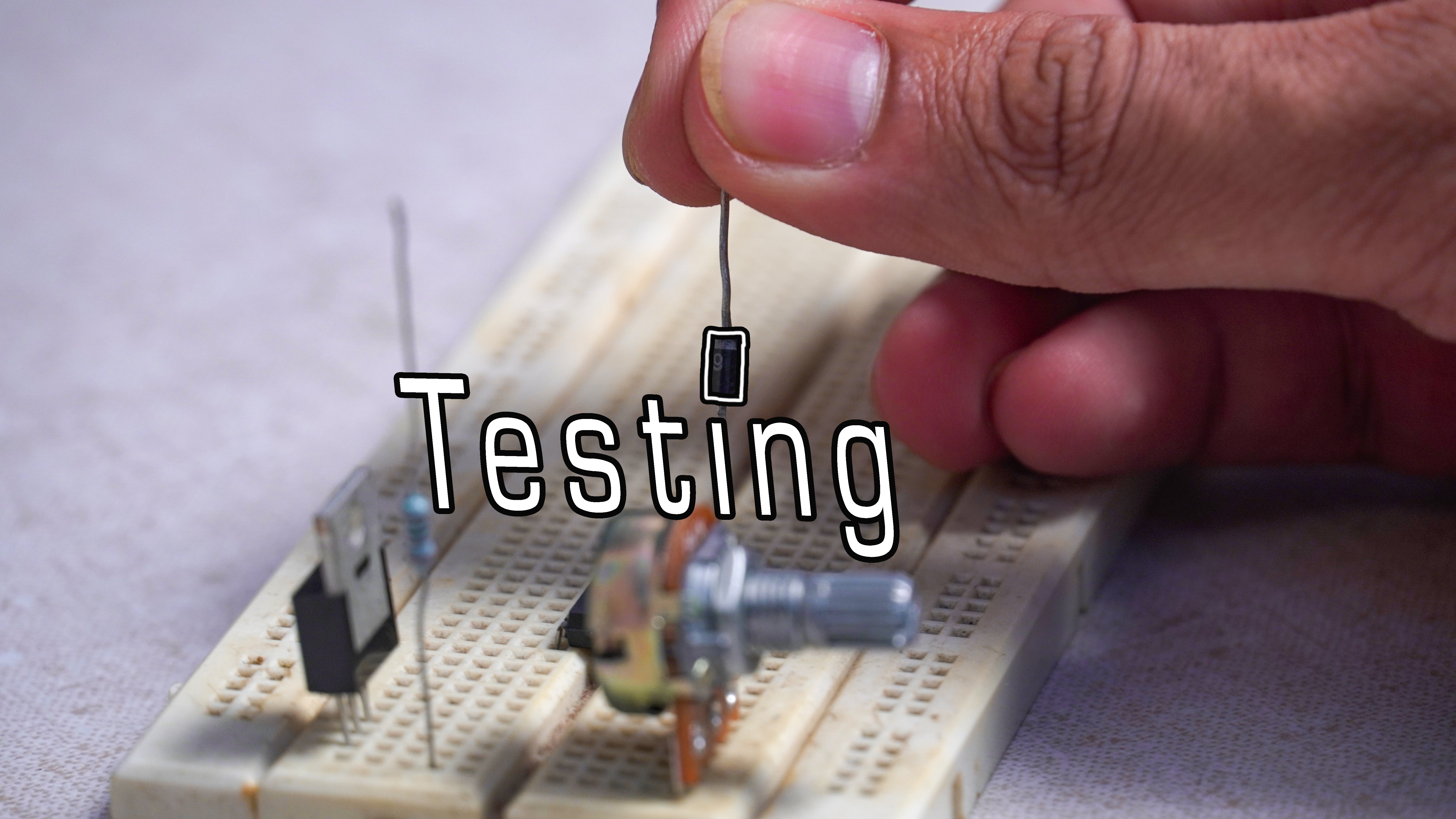
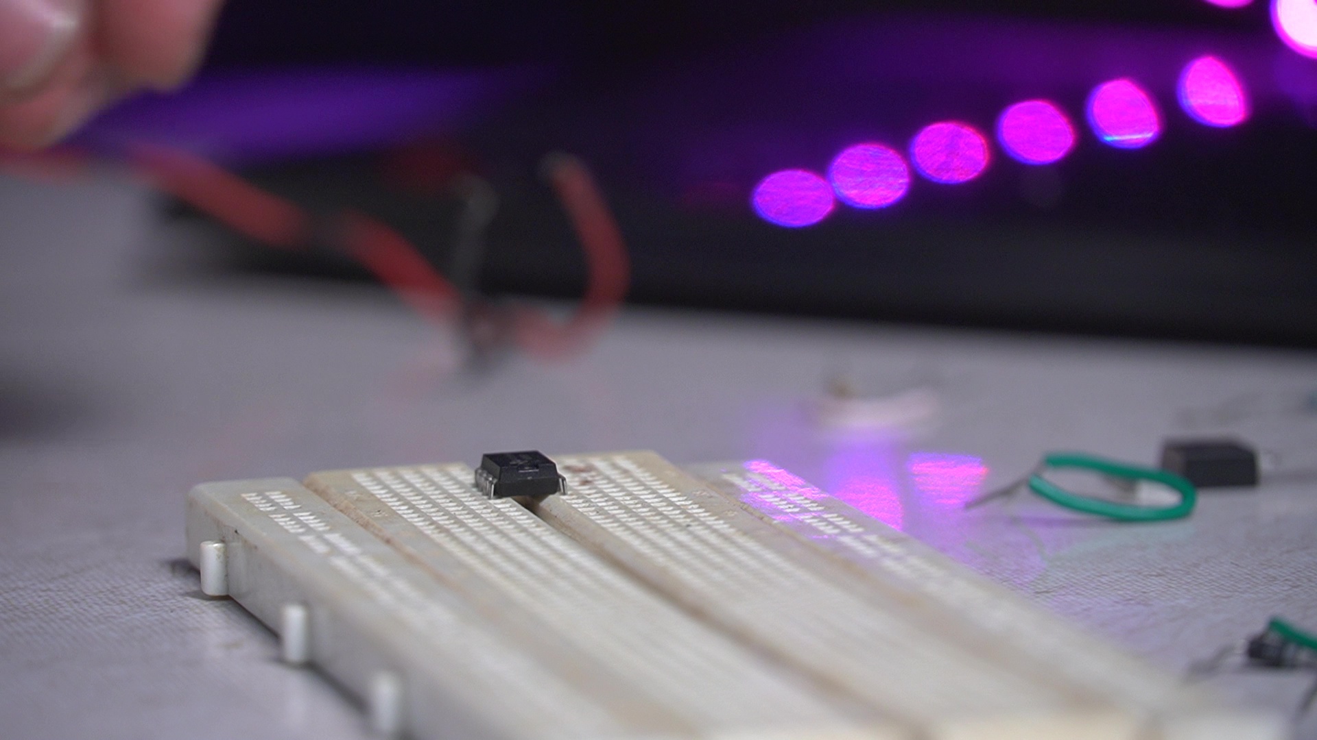
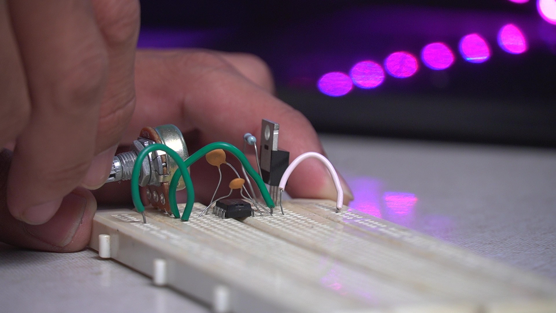
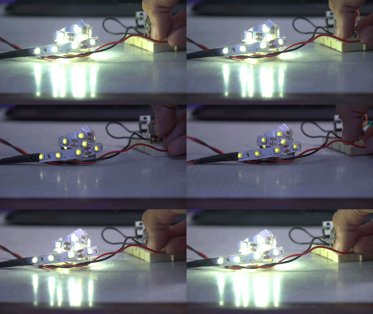
Once our IDEA is finalized, it would be a good idea to implement our circuit in a rough manner using Breadboard.
since we already have our circuit diagram on paper from the last step, we will use breadboard to complete this testing process, if you are new to Breadboard, this post will help you kick-start with breadboards.
simply connect the components according to our circuit diagram, connect a 12v power supply to Vcc and Ground and use variable pot to control the LED intensity at Output.
warning:
the VCC is 12v ( ± 1v ) not 5v, so be careful, at 5v, circuit might not work.
Get Started With EASY EDA
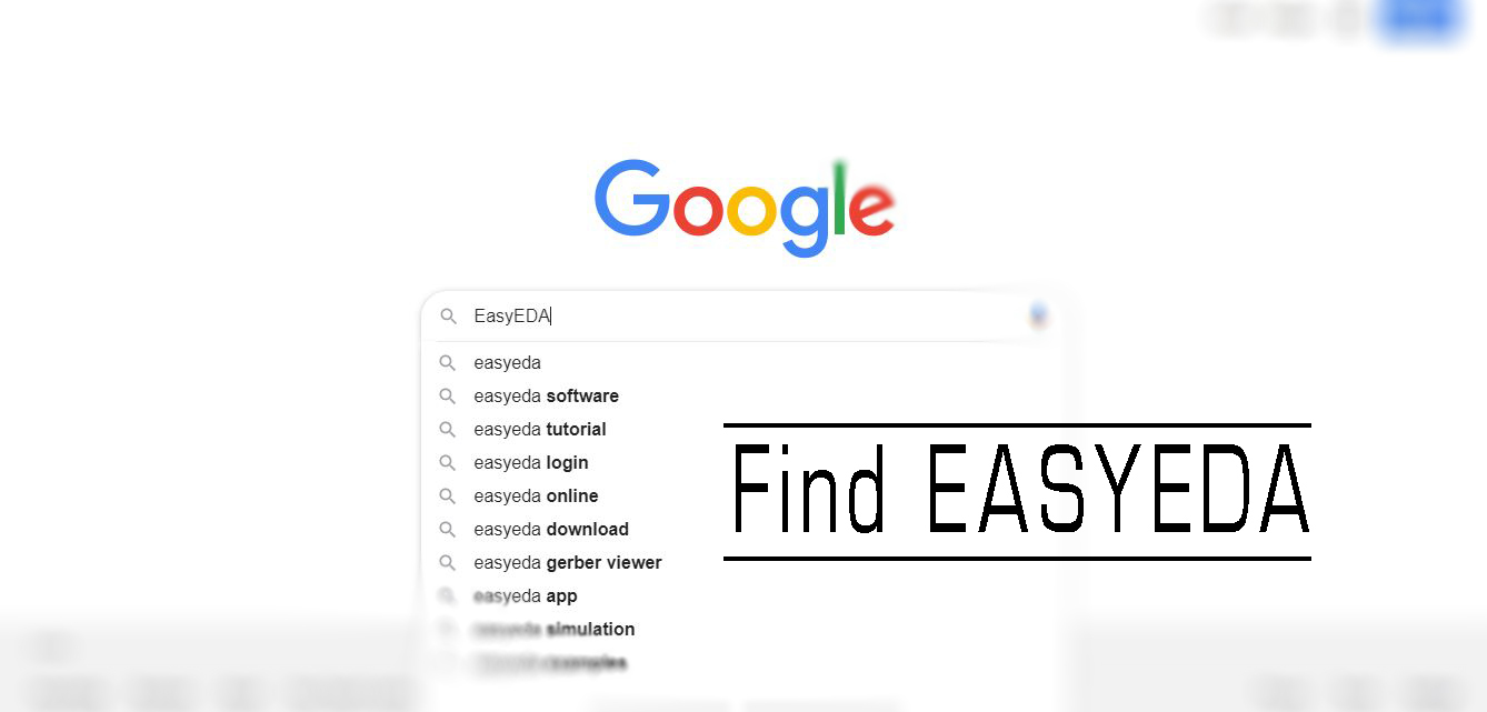
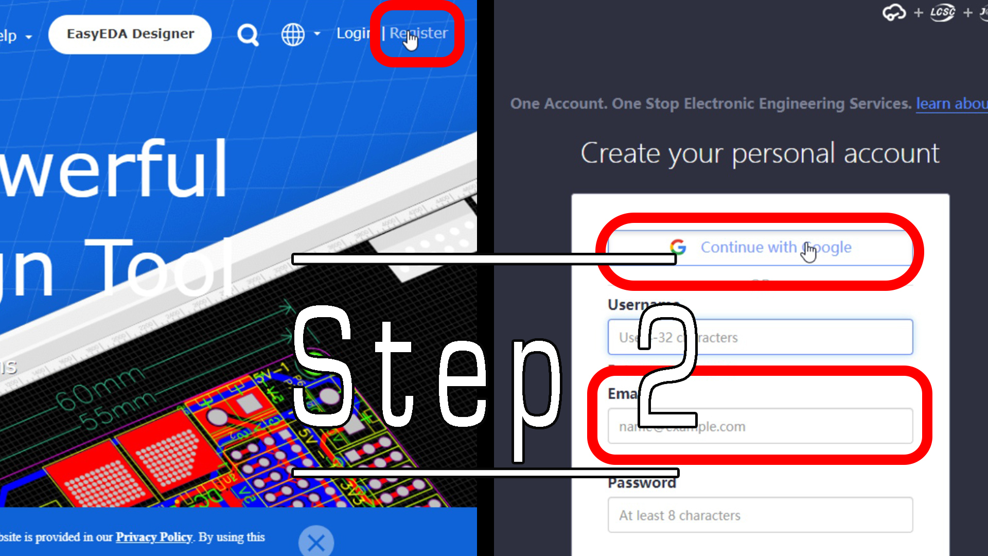
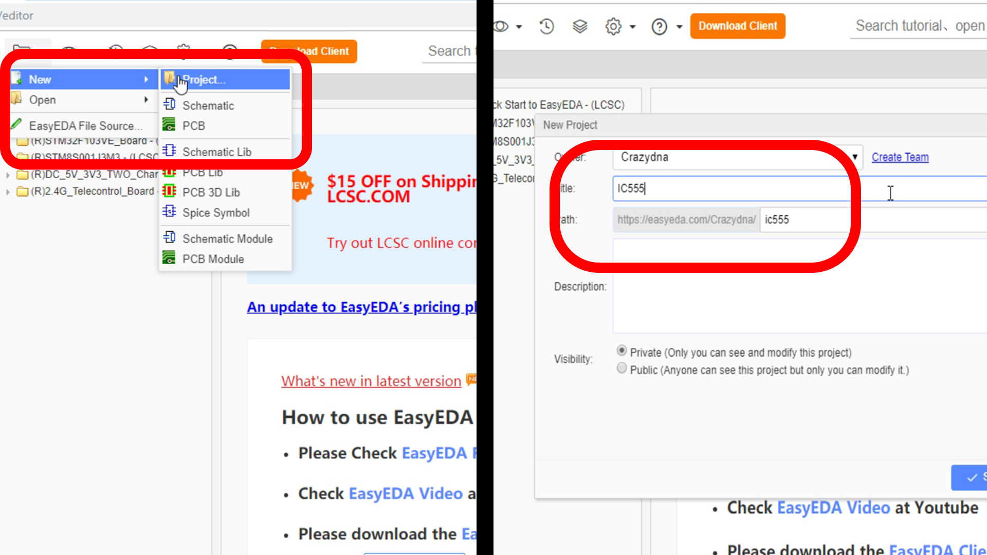
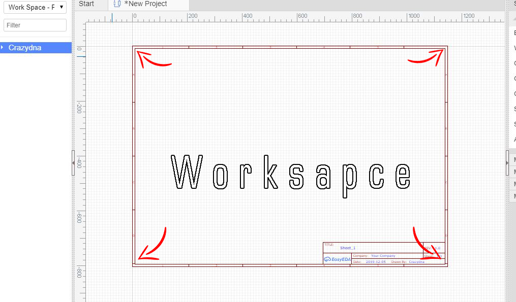
So once we have tested our Circuit, its time start with Software part, so we will first follow the steps mentioned below to get started.
- go to Internet Browser and visit www.easyeda.com .
- click on register, use either Google Account or using Email Address.
- under the Products tab, select Online-Editor option.
- under the Document tab, create New-Project.
- name the New-Project as NE555.
we will see a canvas in the middle of screen, which is called as work-space, we will use it to make a schematic.
on the right side we have tools and attributes, which contain necessary wiring tools and drawing tools.
on the left, we have components, design manager etc, which we will talk in detail further.
Select Proper Components

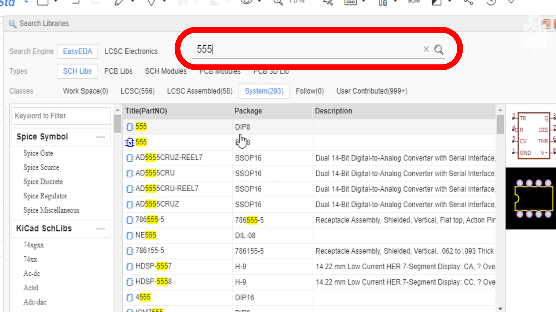
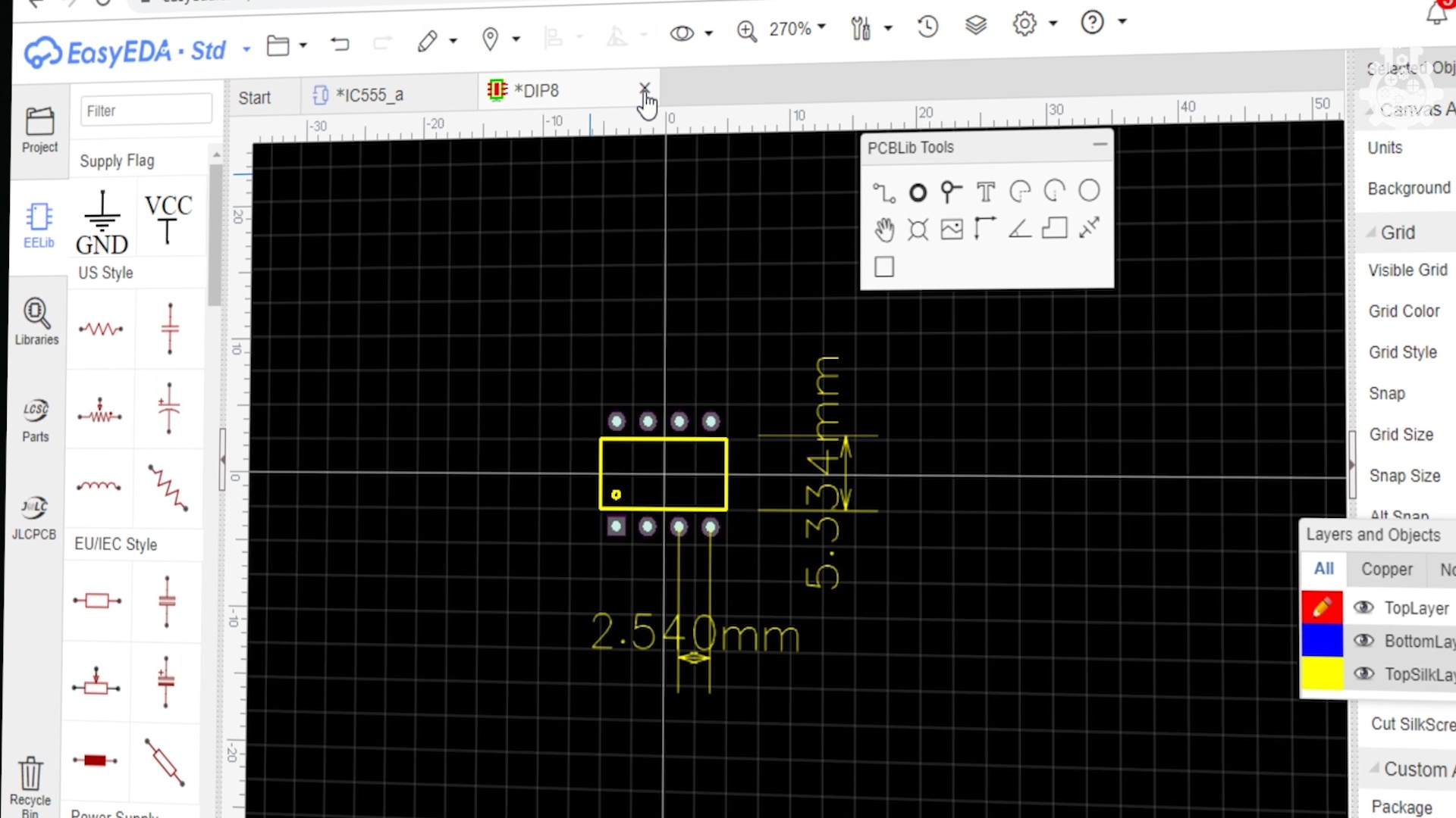
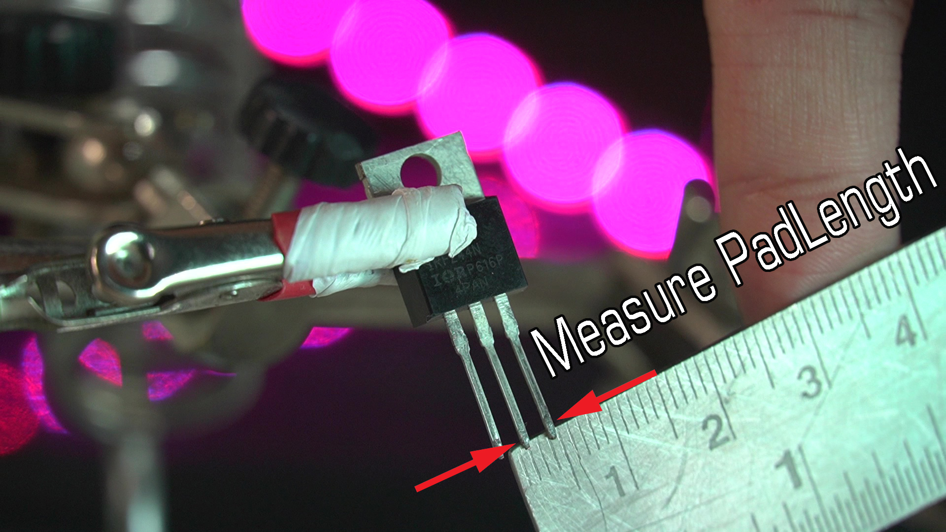
now that we are familiar with interface and we have our project ready on Easy EDA, its time to start building the circuit and import components, but the only problem here is to select the proper component, as every component has different footprint or size. Since we already have our components in hand from the testing on breadboard, we can easily measure the pad distance of each component.
follow these steps to import the correct component:
- open Libraries tool bar.
- in the search bar, look for the required component.
- select visually similar looking component.
- double click on footprint option on left ( which appears in black background on the side of selection ).
- in the canvas attributes, change dimension from mil to mm.
- from PCB library tools, select Dimension tool and measure Pad Distance.
- physically measure Pad Distance of the required component.
- match the Pad distance of physical form with selected component.
- repeat the process for all components.
Pro Tip:
usually the techincal name of components are useful in finding exact component ( for example instead of looking for ic555, we can search for NE555 in dip form factor, which would give more accurate results )
Complete the Schematic
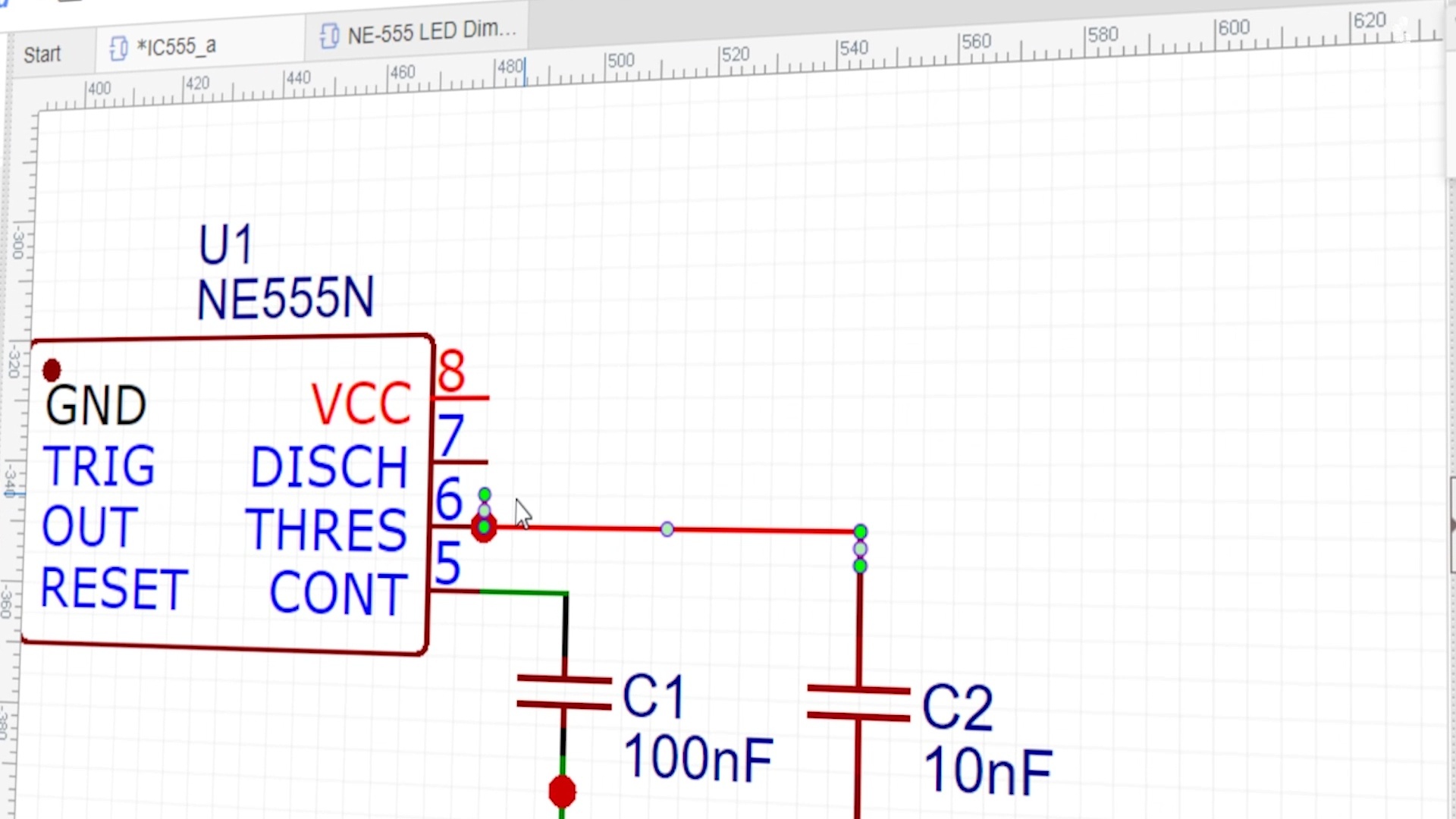
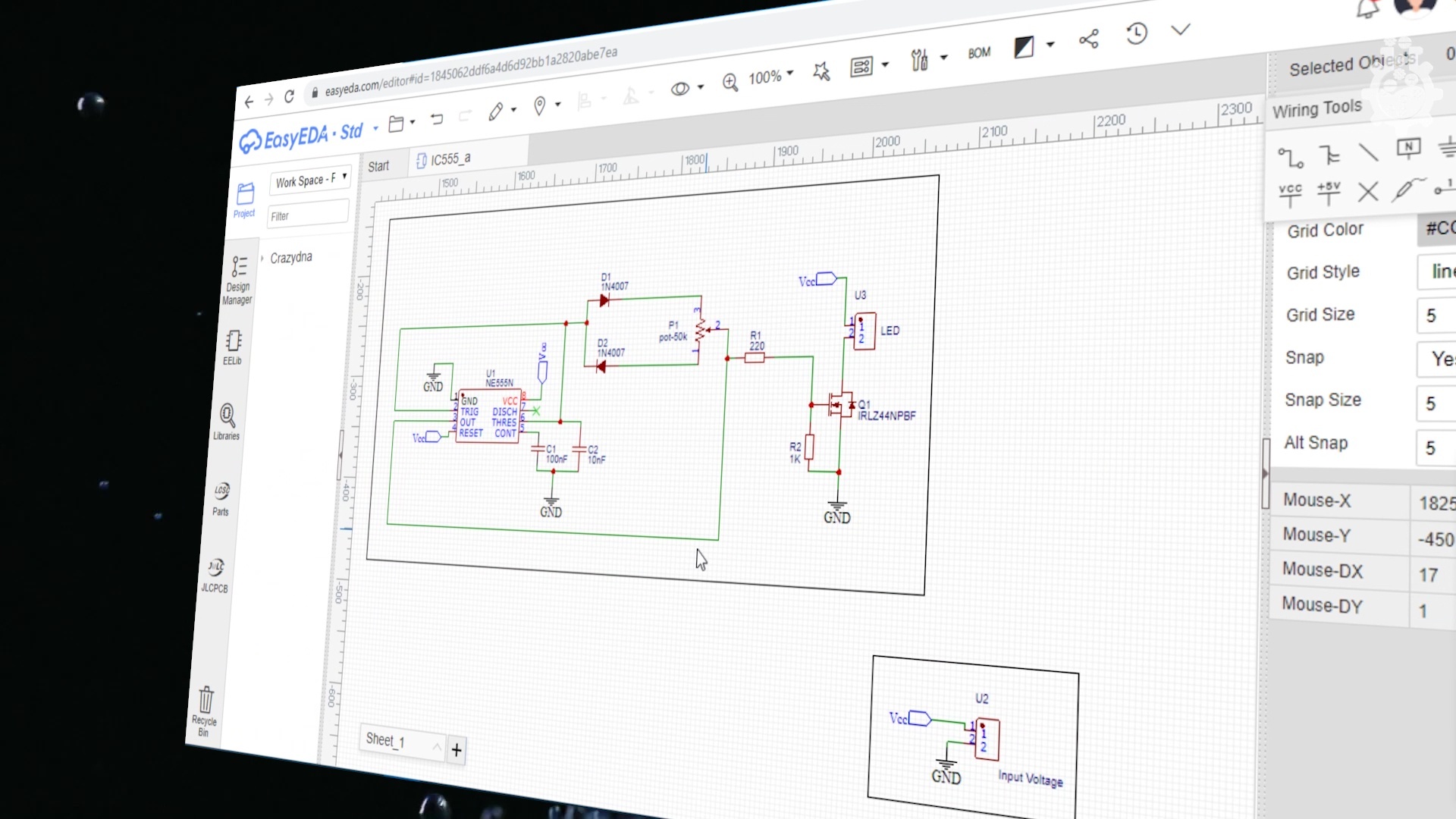
in the last step, we imported all required components on work-space, now we need to complete our schematic to proceed with our PCB design.
we will use wire from wiring tool, while referring the paper diagram to complete all the traces ( i.e connections ).
next we will use Vcc and Ground tools from wiring toolbox, to complete the Power trails of our Circuit.
Downloads
Getting Started With PCB
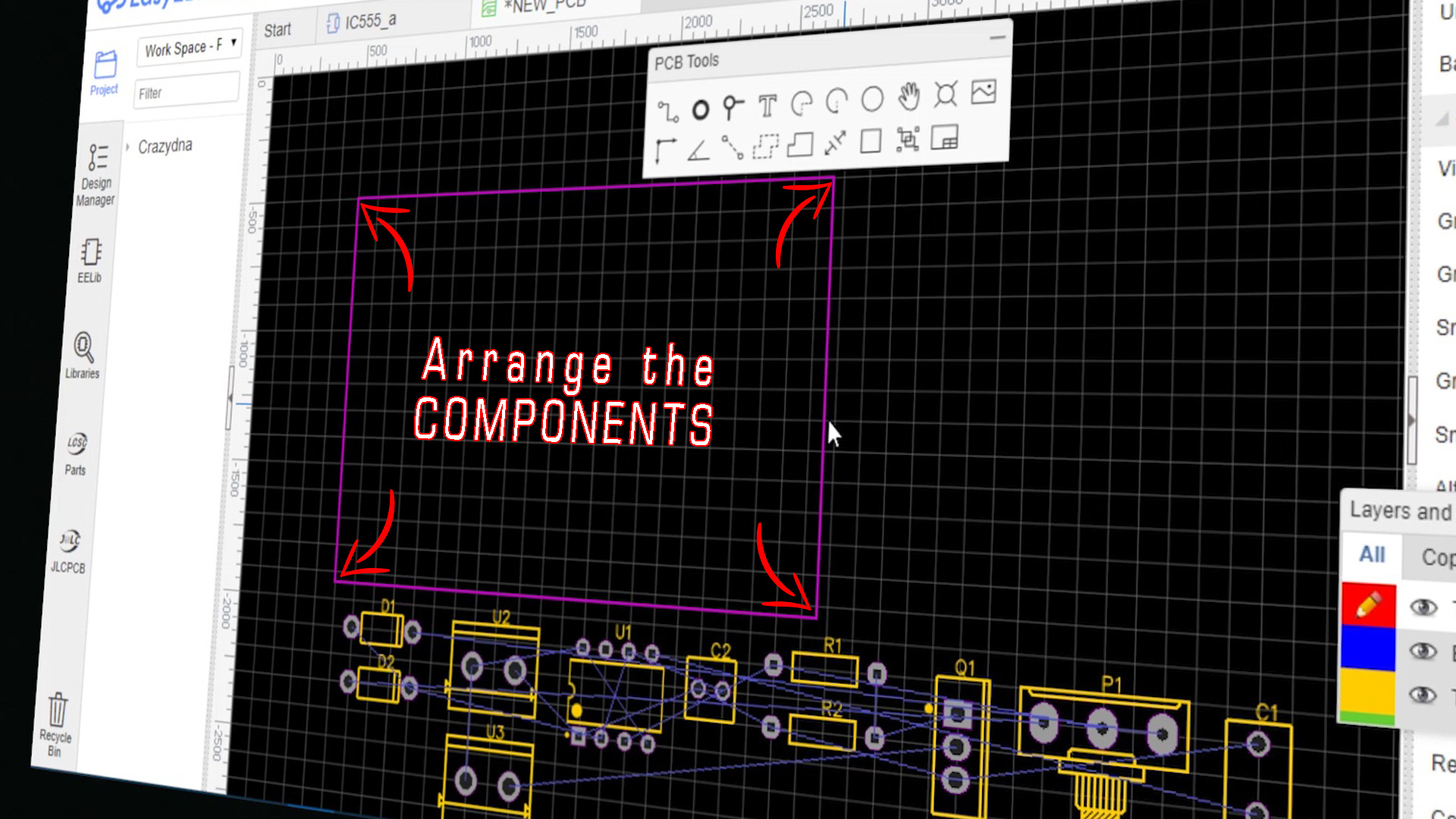
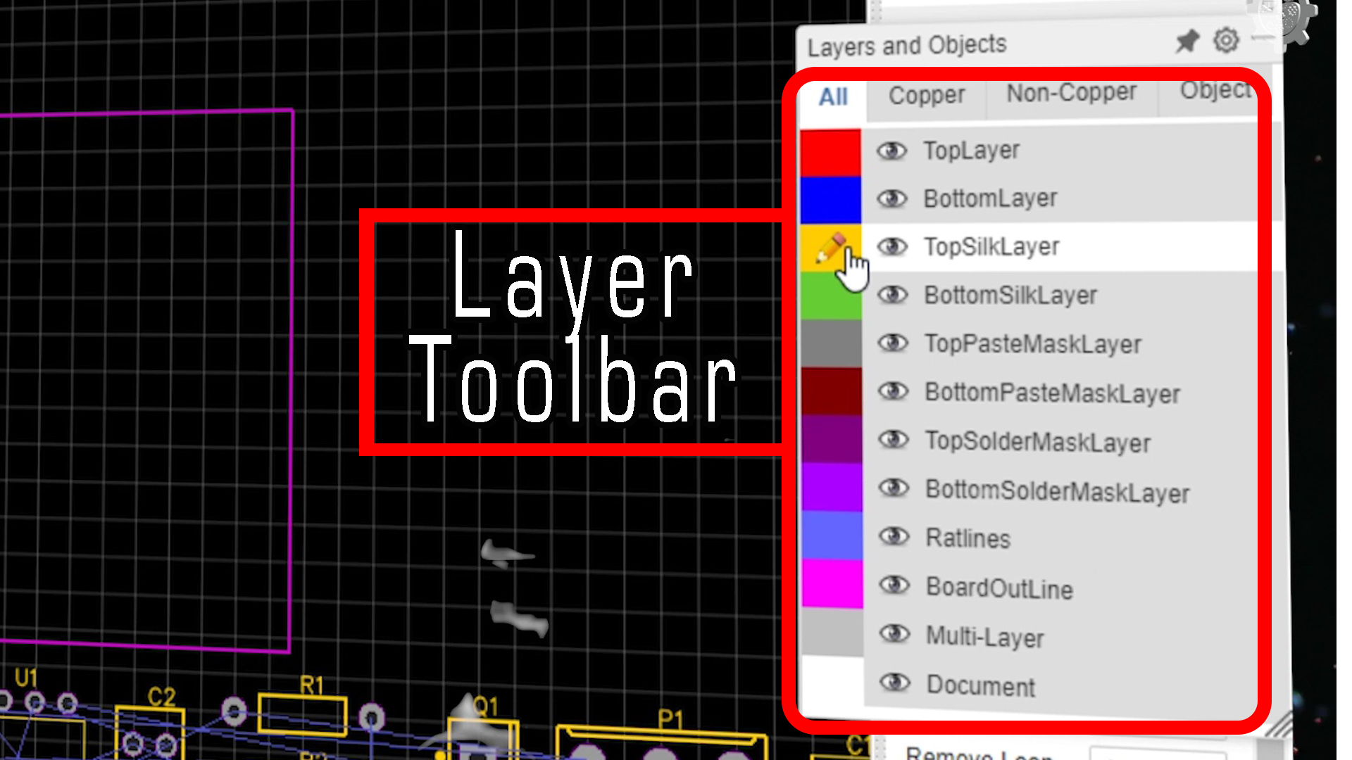
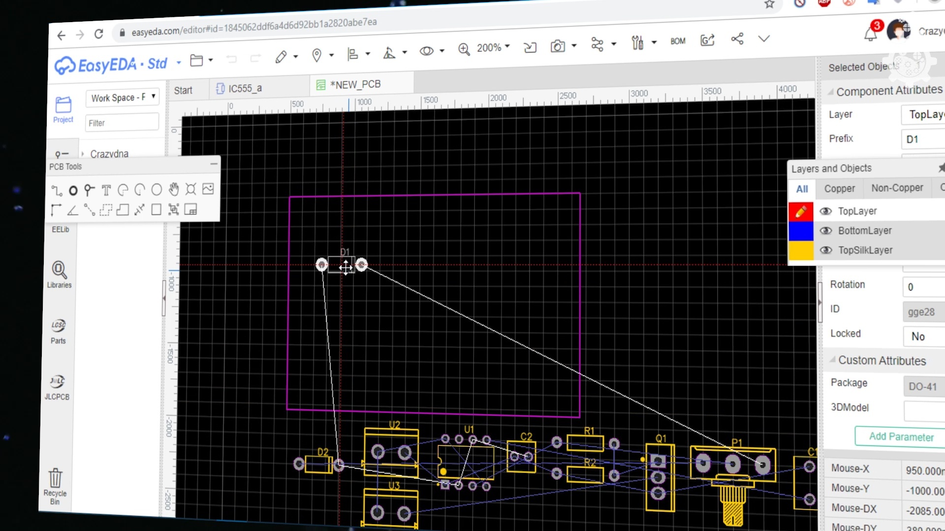
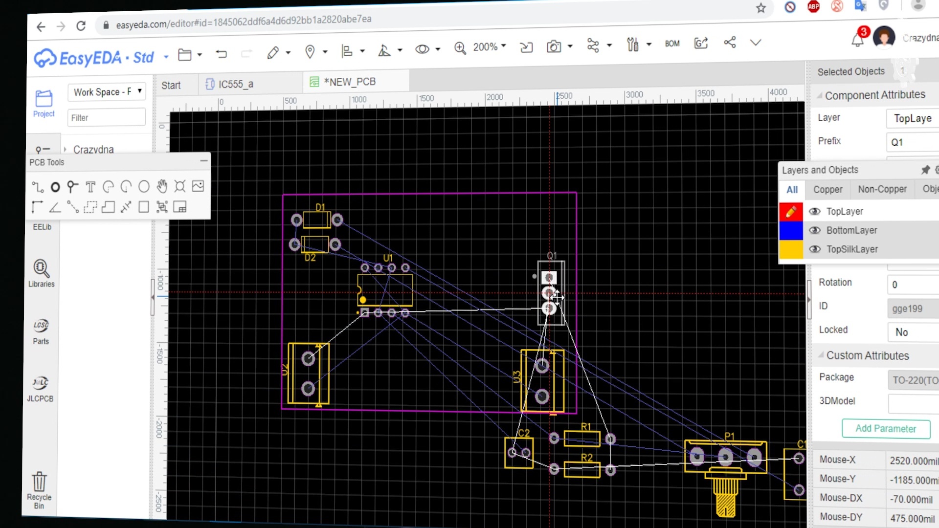
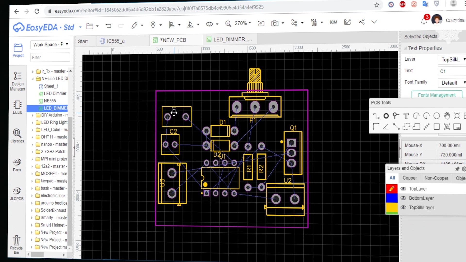
once we completed the Circuit Schematic, its time to convert our Project Schematic into a PCB board, to do so, lets follow the given process.
- save the schematic from last step ( save project file).
- under Convert tab, select Convert to PCB.
in work-space we see a purple box with blue lines, layers sidebar. The purple box is Board Outline, in which the outer shape of our PCB board is defined, the layer toolbar indicates position of layer on which we are working, for example top layer, bottom layer, silk layer, etc.
next we will arrange every component inside of the Purple Box ( i.e Board Outline Layer), according to space allocation.
Pro Tip:
don't Overlap any components, it will cause design rule errors.
try to keep sensitive components near to IC chips ( for example in this circuit, keep capacitors near to pin 5,6 of ic)
Complete the Traces ( Routing )
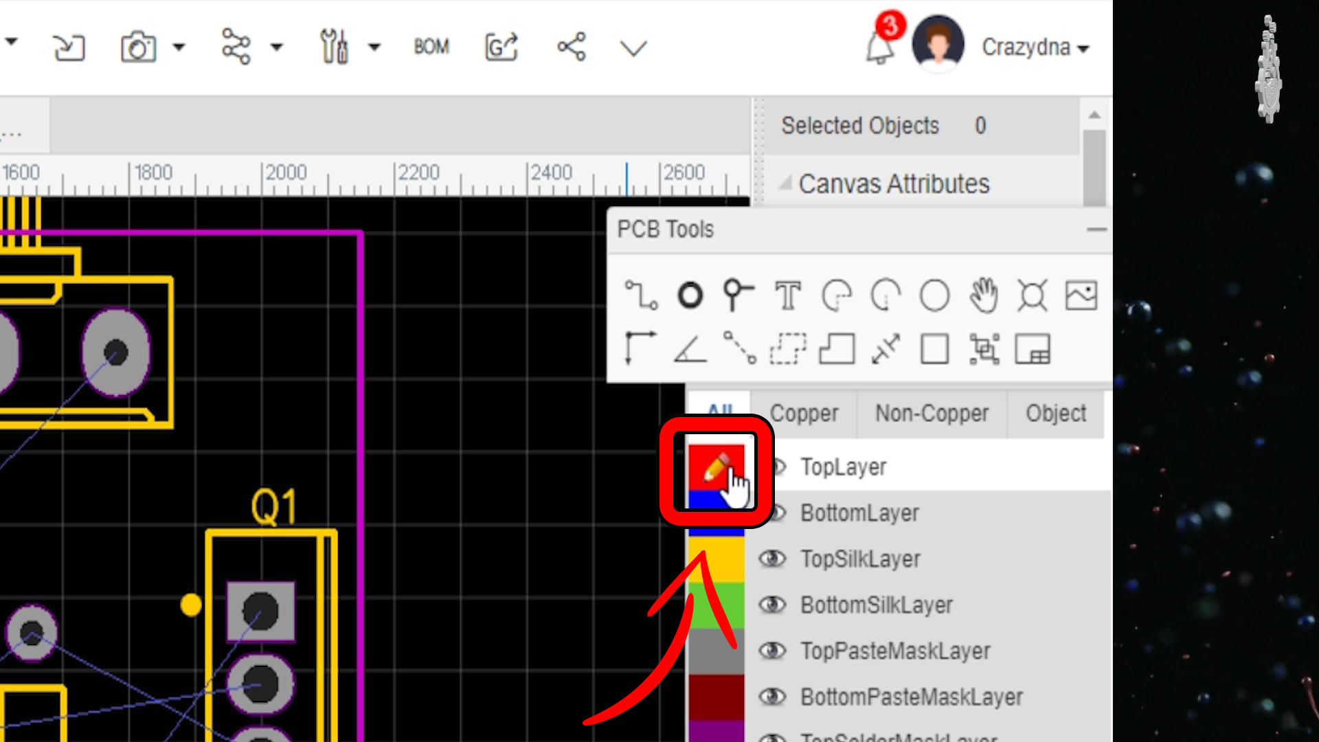
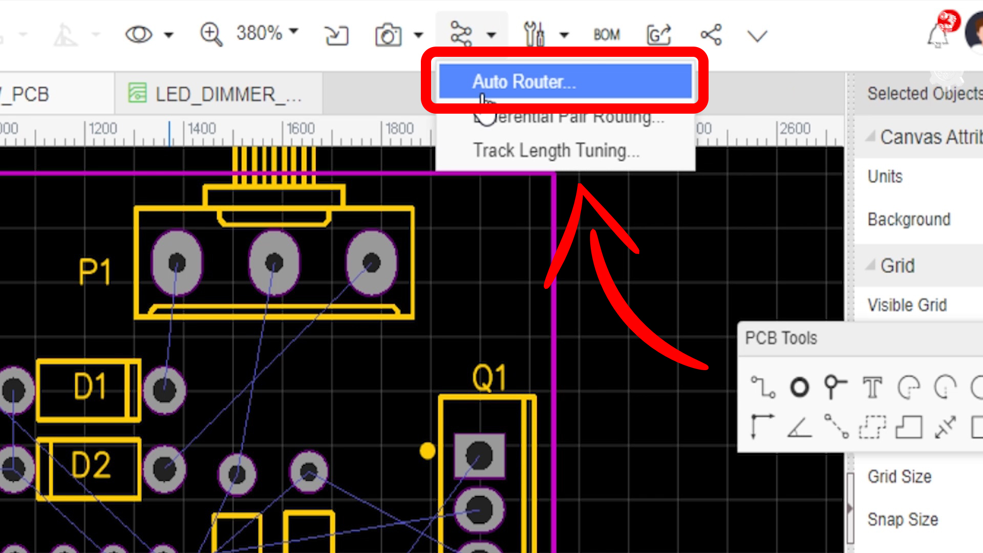
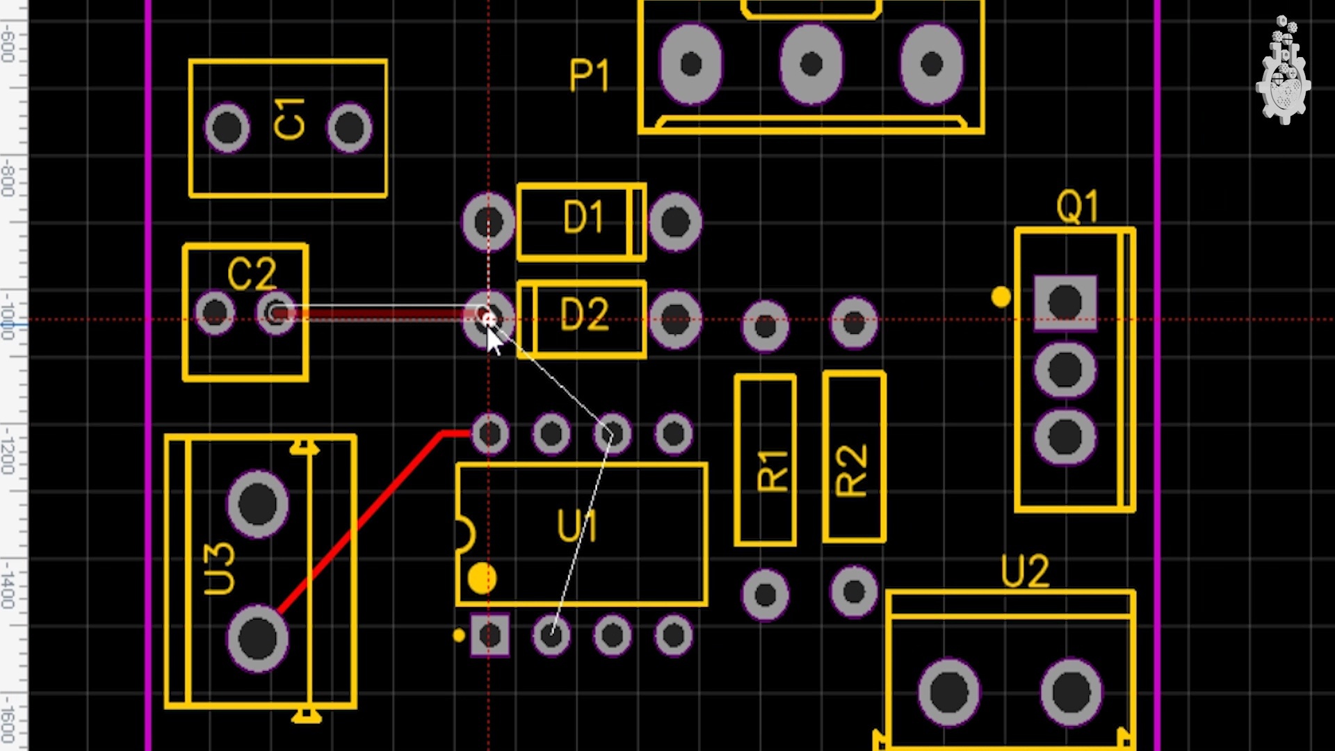
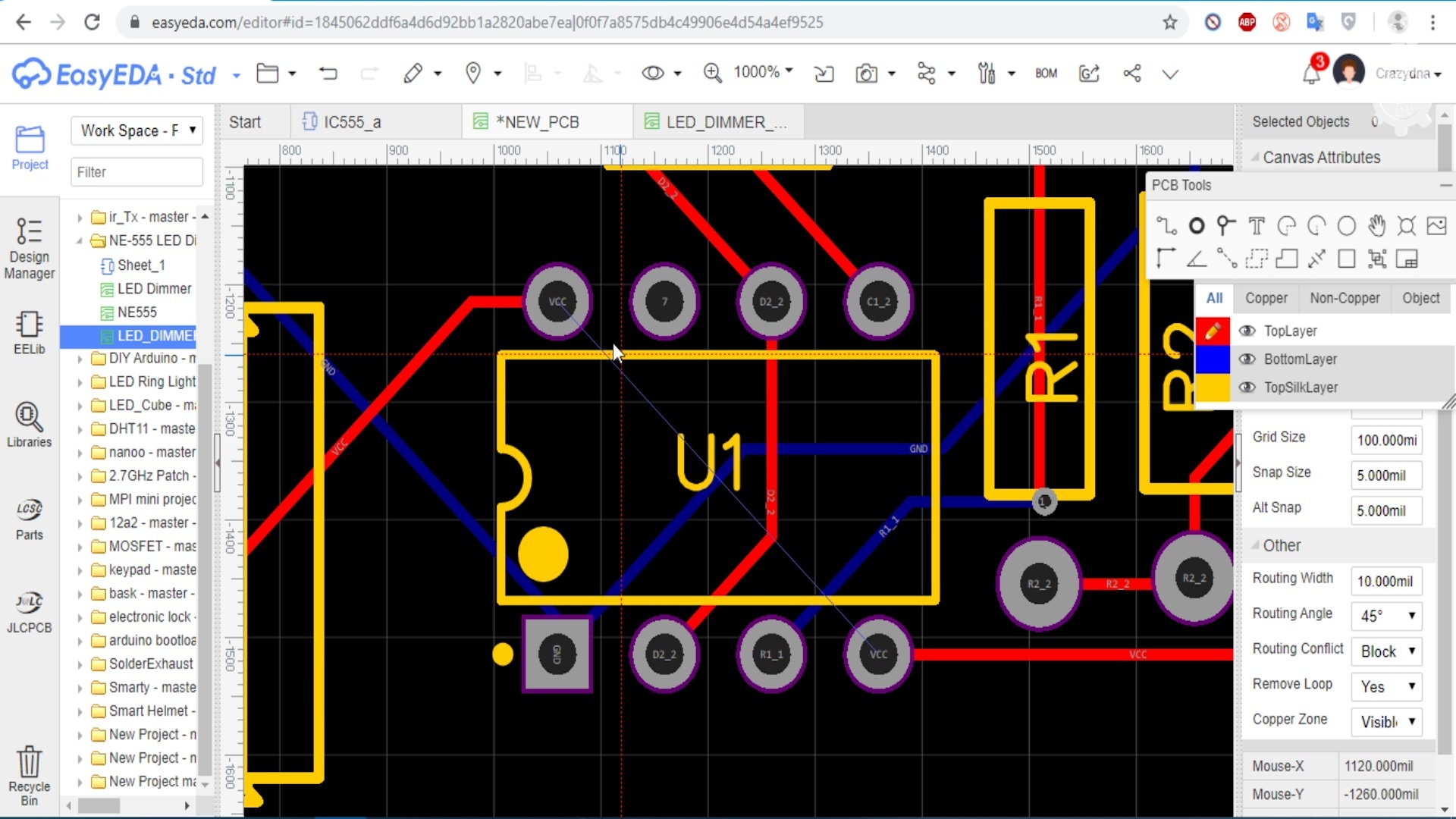
now its time to complete our PCB traces, we have 2 options here to do it, that is Auto Routing or Manual Routing. since Auto Routing is not the best option and can cause unnecessary errors, so we will do Manual Route in this Example.
for Manual Routing, follow these steps:
- go to top layer by clicking on pencil icon near the toolbar.
- go to PCB tools and Select Track Tool.
- connect one pad to another, following net wire ( i.e. blue wires) once done, blue net wire will disappear.
- go to bottom layer by clicking on pencil icon near toolbar, and use bottom layer when required.
- adjust Board Outline according to need.
Pro Tip:
use via when ever stuck between two layers.
keep an eye on Nets for faster connections.
Export Gerber
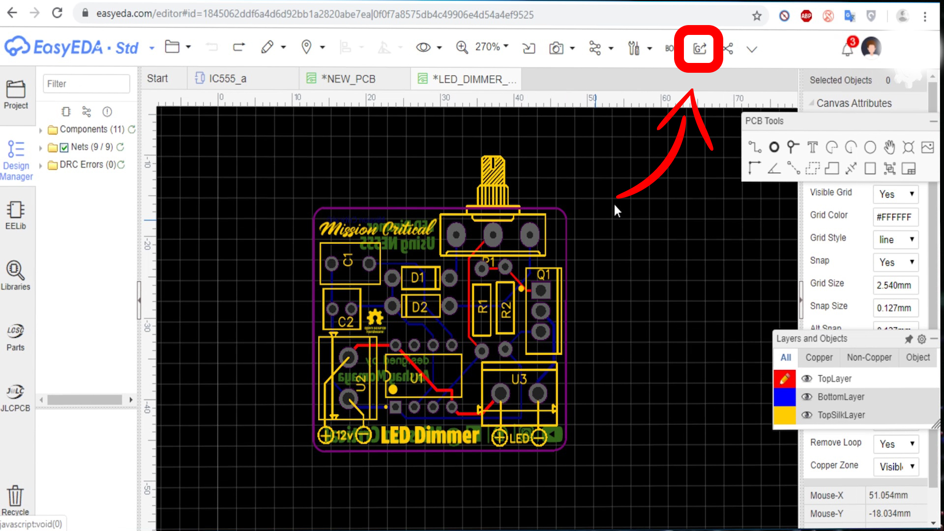
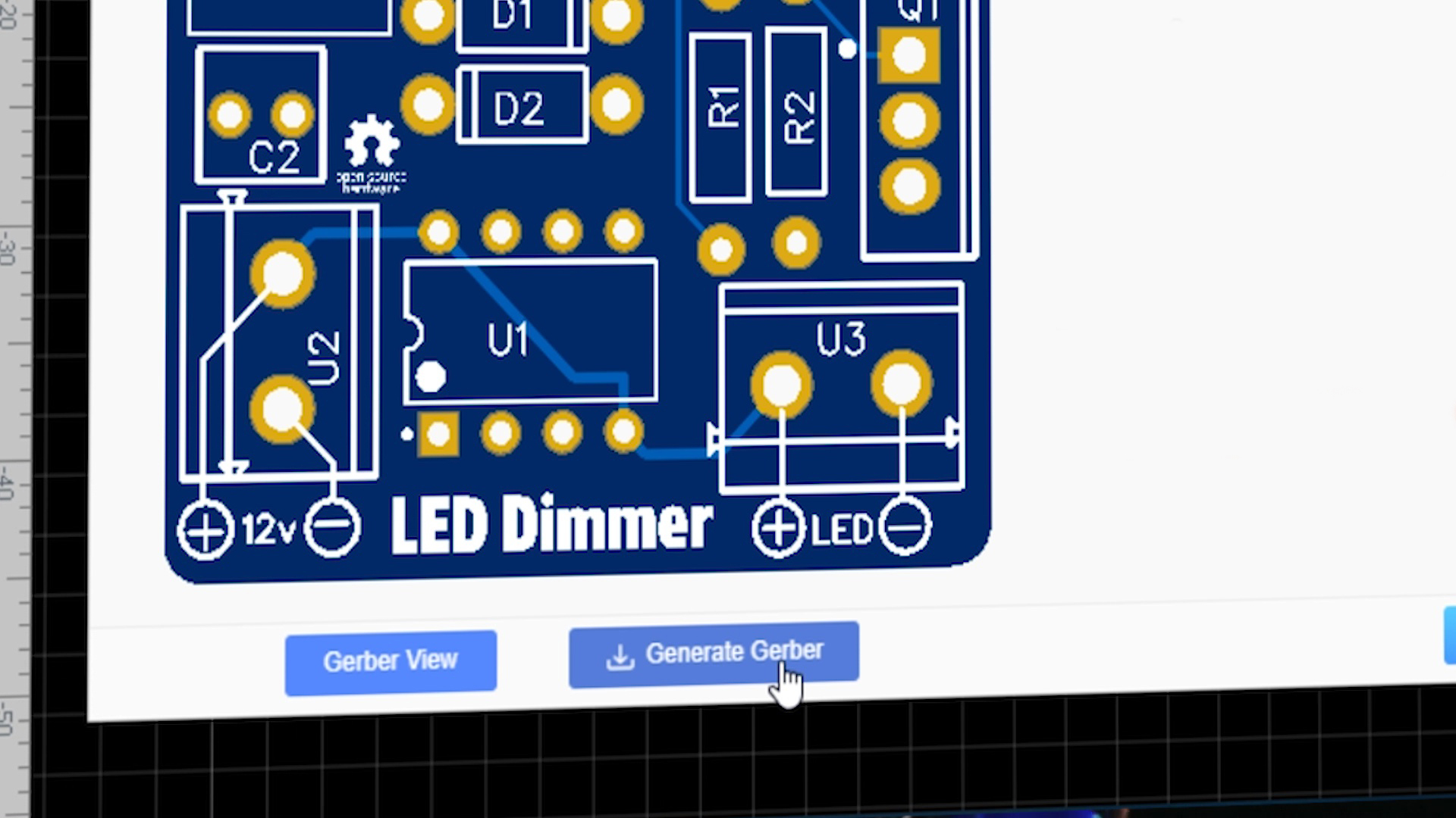
save the previous PCB design inside the project and proceed further.
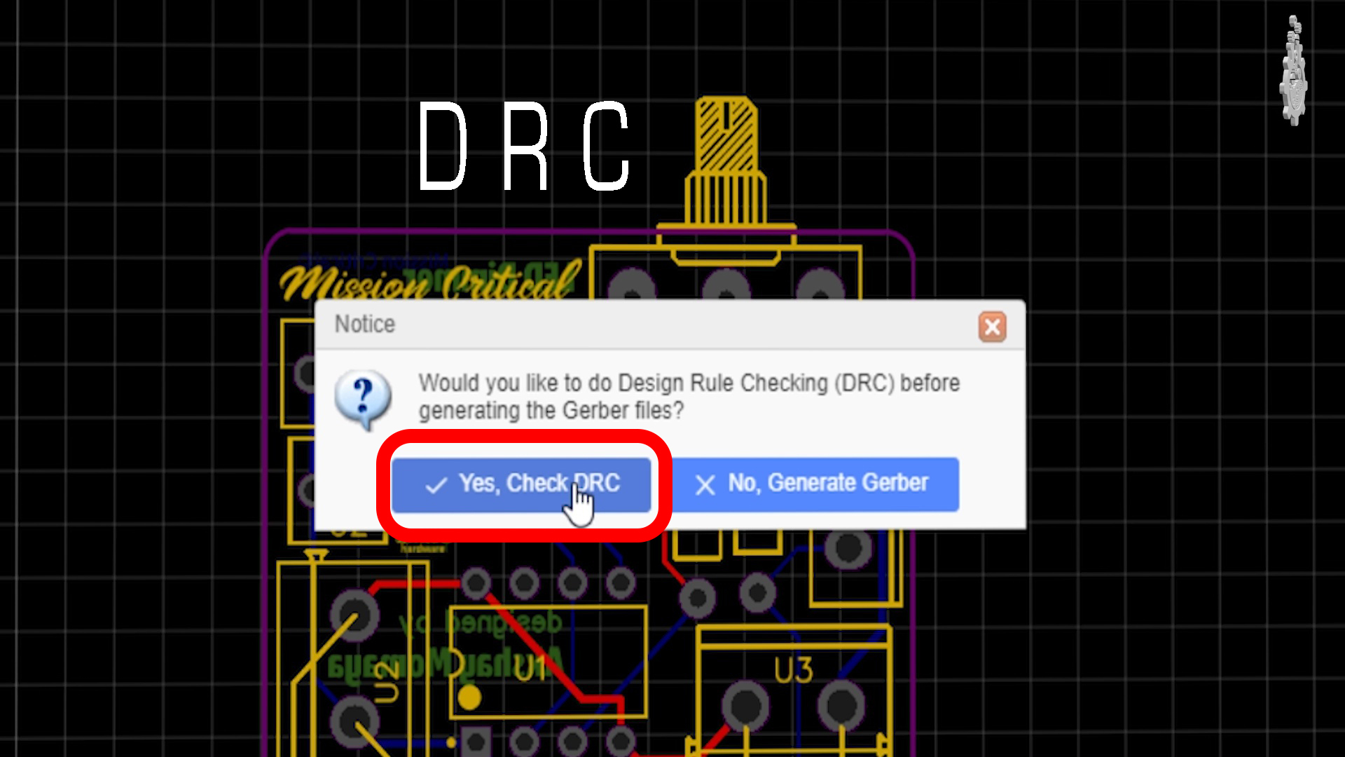
but there are few rules to be followed, provided by PCB manufacturers and or general designing rules, but those parameters are quite advanced, so let's keep design rules Standard and continue to perform a Design Rule Check (DRC check) this DRC check will make sure we don’t have any error in our design.
to perform DRC check and Export Gerber file, simply click on " Generate Fabrication File " icon and it will prompt to proceed for DRC check, after that, simply save the Gerber file on Computer.
Manufacturing of PCB
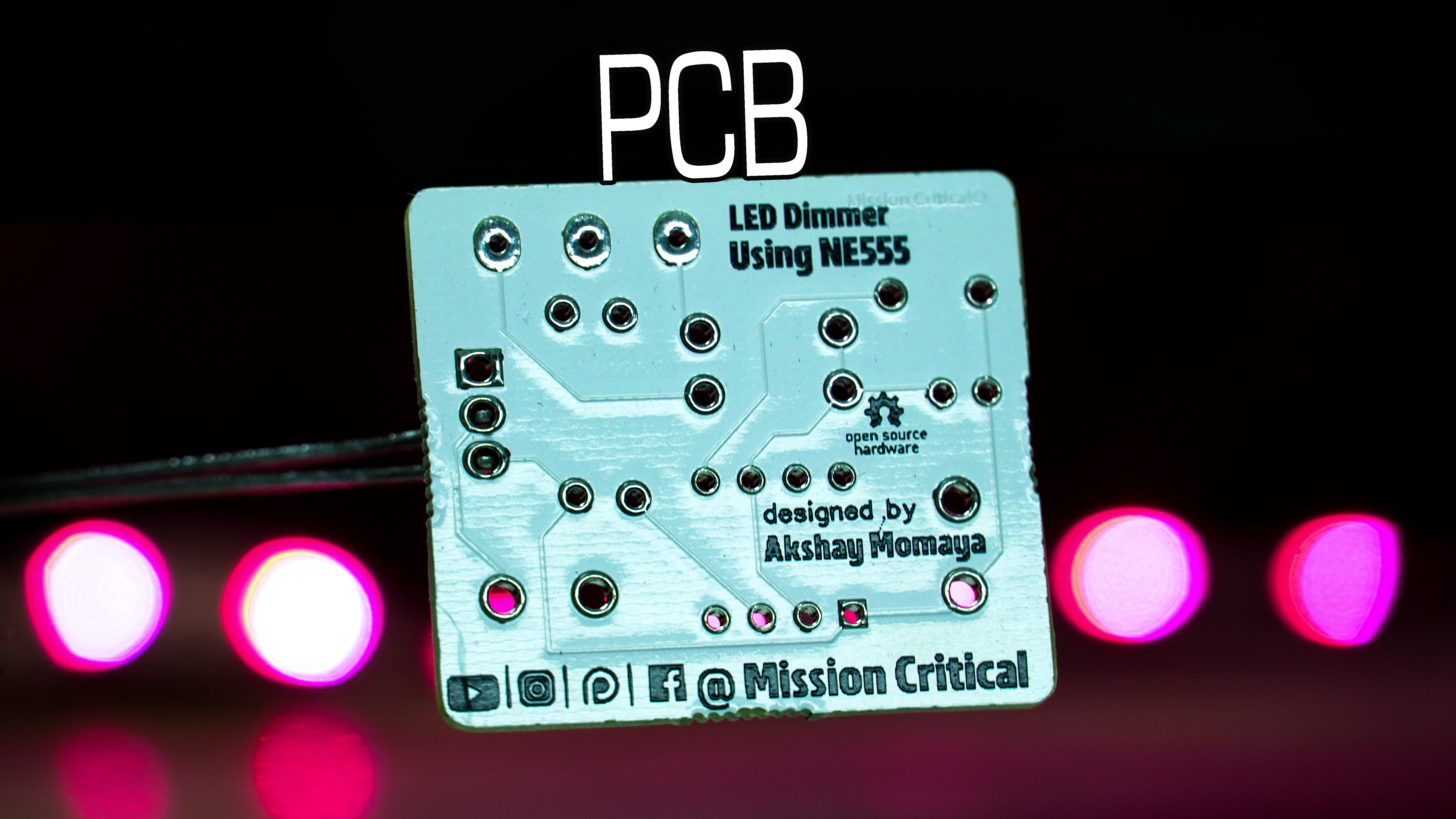
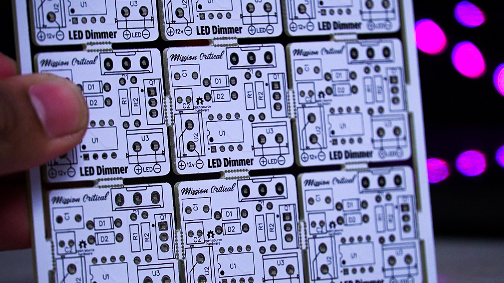
we can either manufacture PCB at home or Order them online by any PCB manufacturing services.
to manufacture a PCB at home, we can follow this post , but it is neither easy, nor precise to make a PCB at home, so i would suggest Online PCB Service for PCB manufacturing.
ordering a PCB online is very simple, we need to follow the given steps:
- register on the online pcb service website.
- enter the Dimension of PCB
- enter the No of Layers.
- enter the Quantity of PCB.
- enter the Thickness of PCB.
- Choose Silk layer color.
- keep all other specifications same as standard.
- select Shipping Method.
Pro Tip:
order multiple PCBs together to save shipping and Import Taxes.
Test the PCB
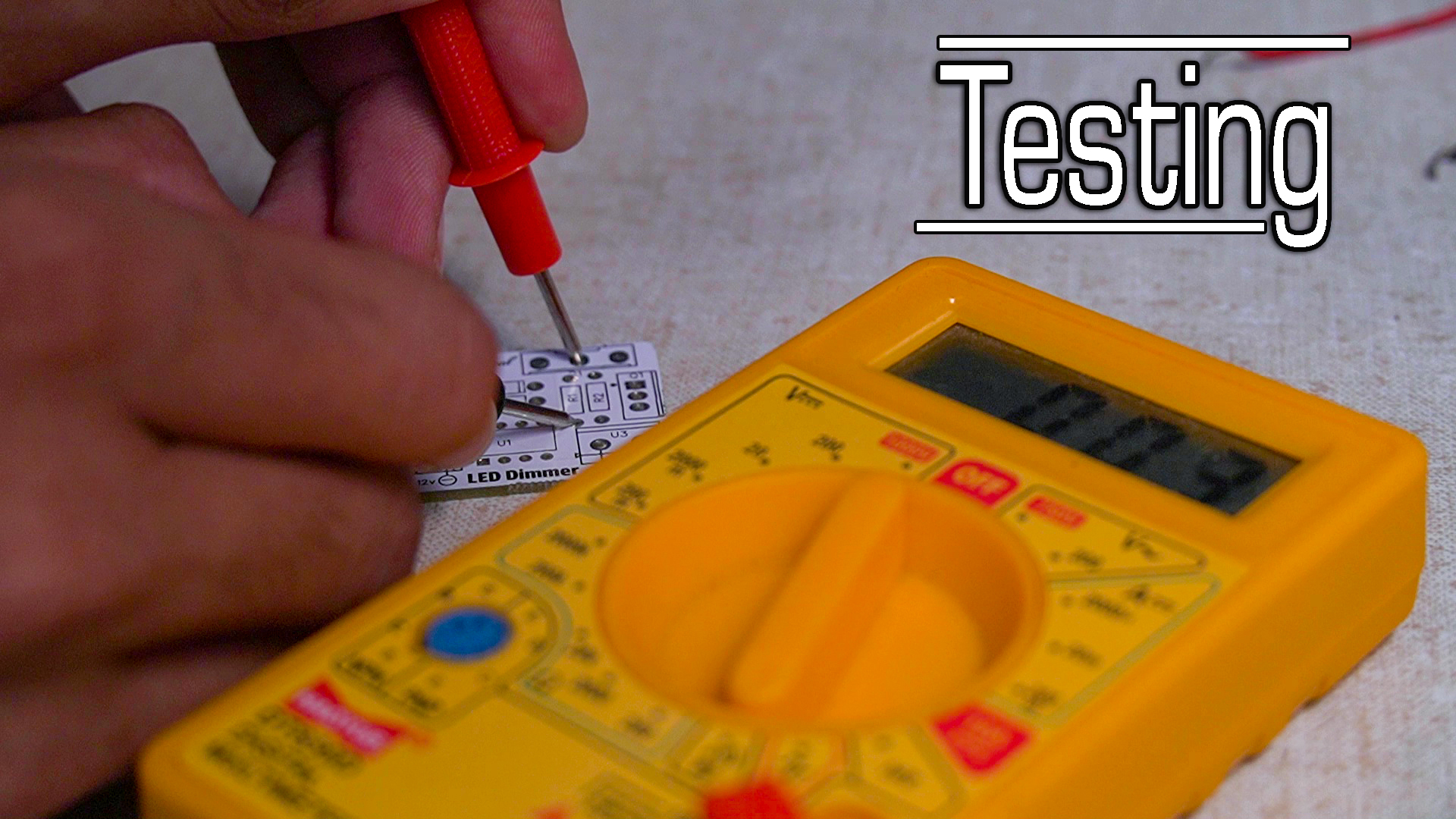
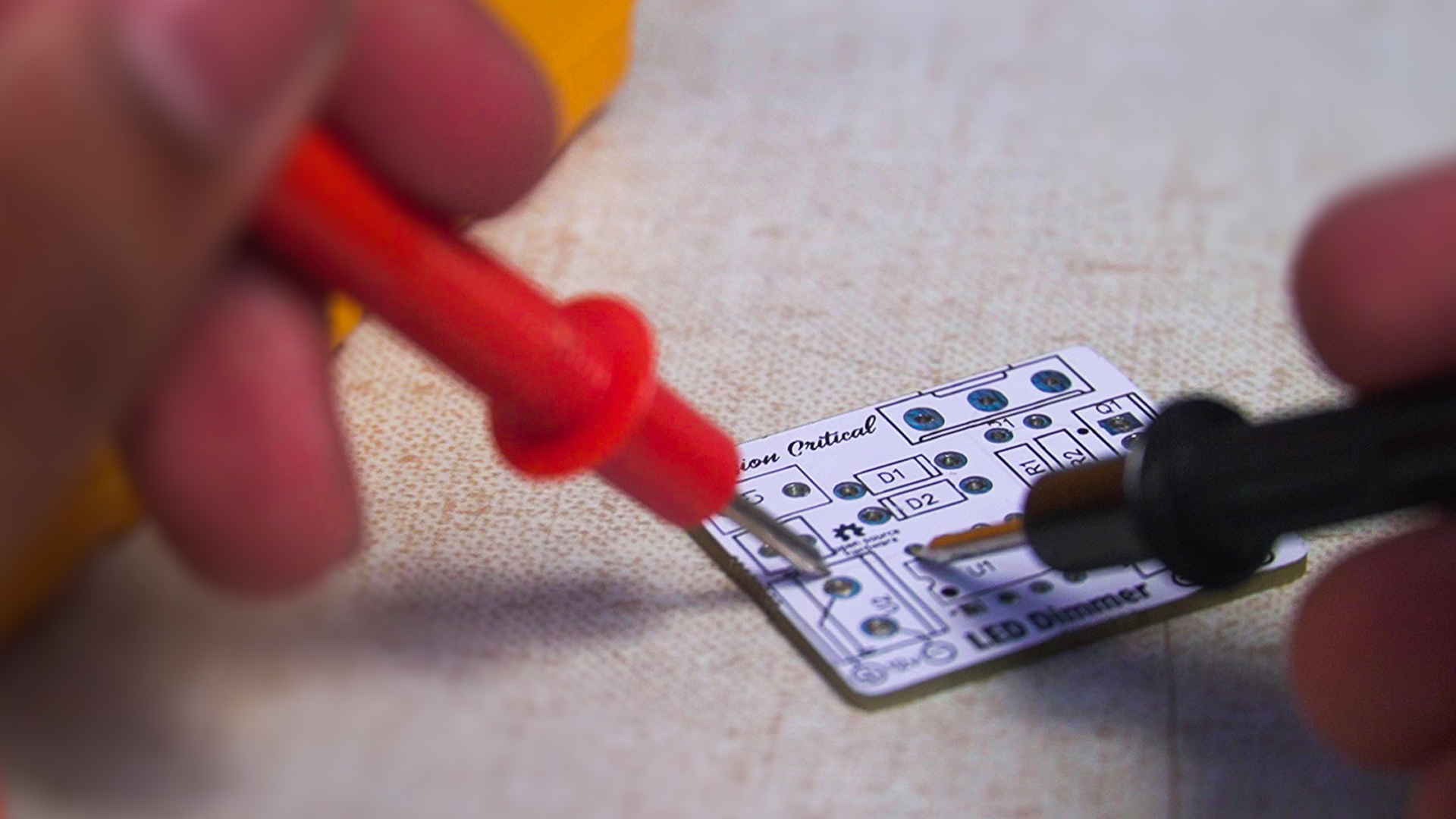
once the PCBs reach our Home/ Lab, we need to test them for defects or any problems, to do so, we will follow these steps:
- set the Mutlimeter to Continuity Mode.
- Probe One END of DMM to Pad A ( pad A is any point of Contact of Connection ).
- probe Other END of DMM to Pad B ( pad B is the point which is supposed to Connected to Pad A).
- check each connection points.
Sodering
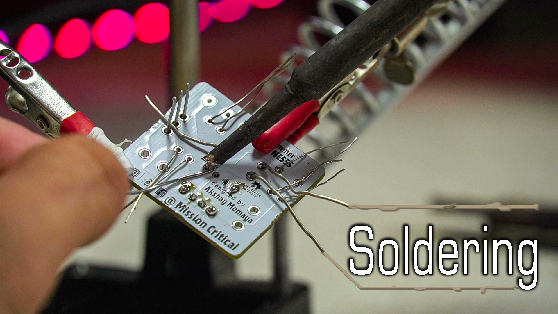
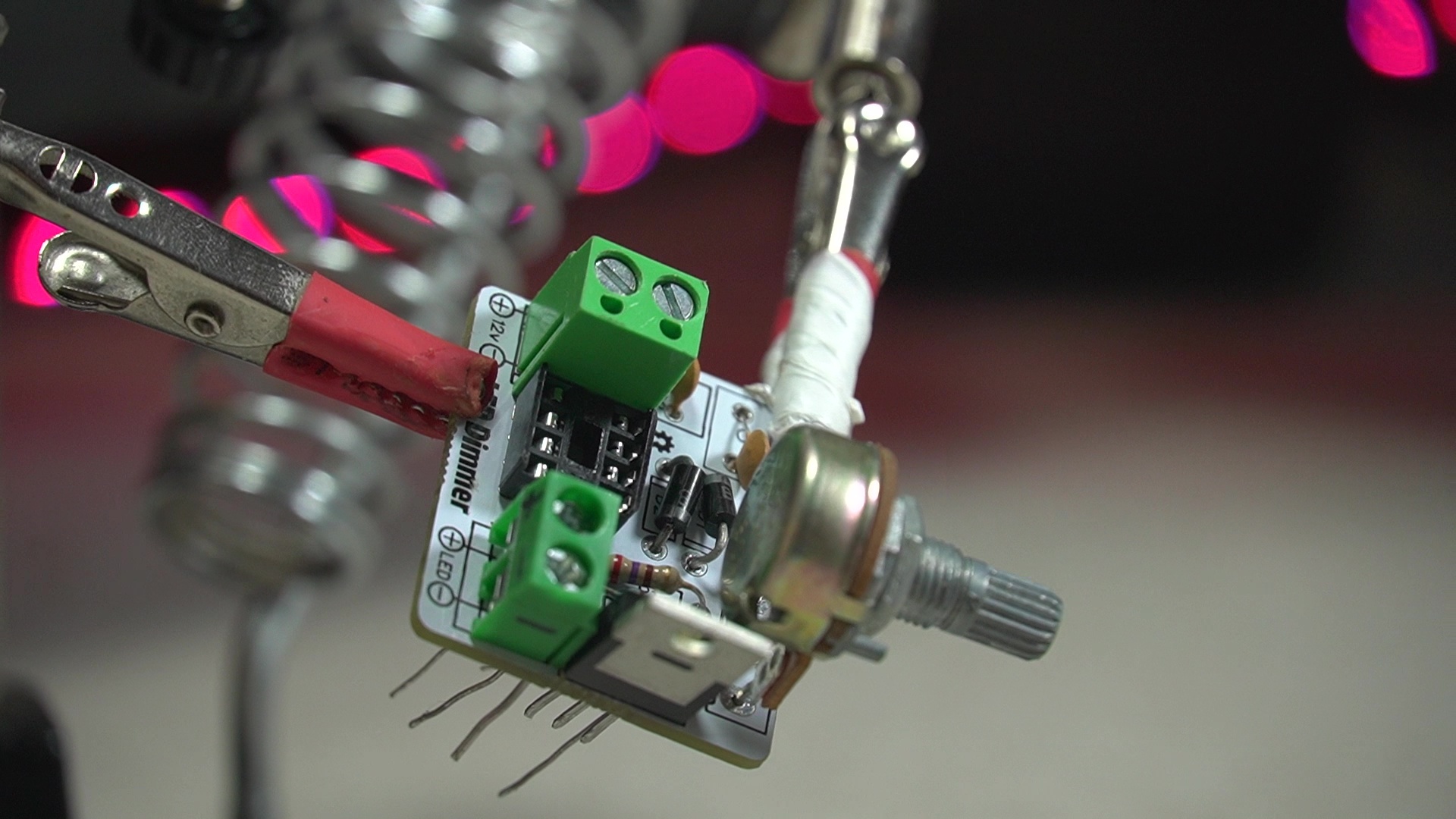
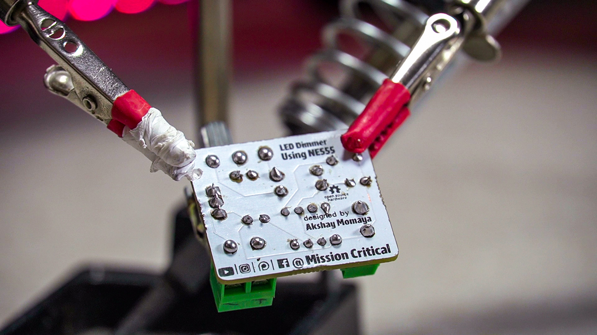
once we are satisfied with PCB quality and design, its time to solder each component into its allocated locations.
since we used components with Footprint as Silk Layer, we have a notation of each component, all we need to do is to check the schematic and identify component, insert them in correct orientation and solder them.
if you are a beginner, you can refer this post for THT soldering and this post for SMD soldering.
Thank You :)
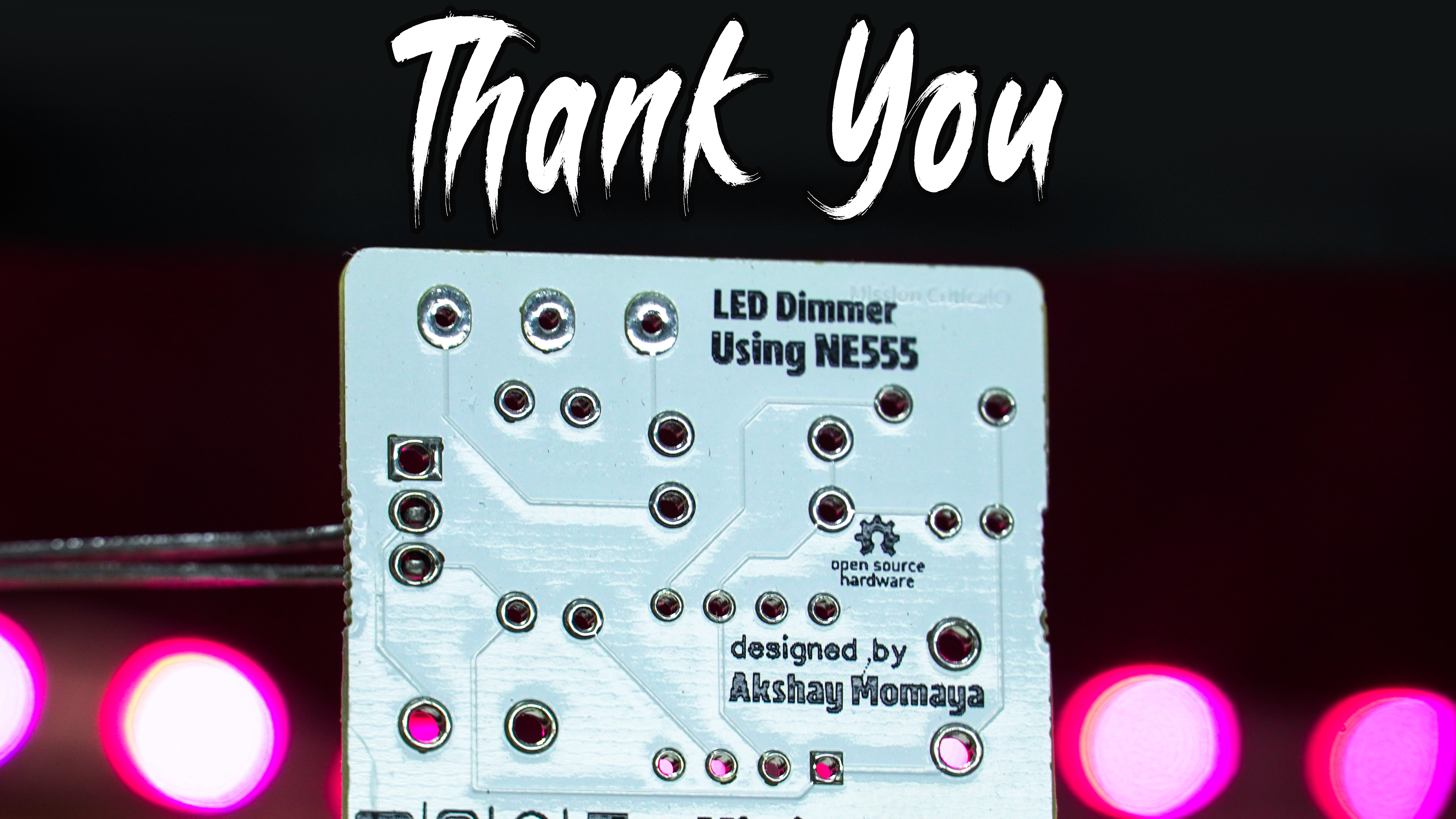
if you followed up this post, and liked it, make sure to check out our other work on youtube,
you can also support us for following Mission Critical on social media or becoming our patreon.
Patreon - https://www.patreon.com/missioncritical
Instagram @officialmissioncritical