Grid Tie Inverter V4

I wish I could present to you a working 250 W grid connected inverter. Alas, one of my MOSFETs violently exploded during some tests and took down some other components with it. I wanted to give up on my whole ambition to develop an open source 1kw hybrid inverter. However after a few days my enthusiasm has rekindled. This can be done, I will do it, but perhaps in a subsequent version. Since I wrote this report as I went along, I have published this failed attempt regardless. I have definitely made ground since version 3 so I hope it has some useful information in it.
The code and design files are all on GitHub along with the pdf version of the writeup.
Downloads
Introduction
Grid connected inverters are fascinating circuits and I have long dreamt of building a well documented open source implementation. They are not trivial circuits to build because they contain high voltages, fast switching transients and safety critical software. This is my 4th attempt…
I had not found a single nuts & bolts approach to making such an inverter until I stumbled across a great one on Instructables by a chap called Poldo. He writes well and has great videos explaining his 100W current source inverter. He employs a fairly different approach to the one presented here. His writeup is well worth a read.
I believe an open source, well documented, 1 kW inverter would be interesting so despite still being a fair way off, I am making efforts towards this. I think the DC Bus could be generated by a separate module which would allow overall flexibility in terms of input voltage range, hybrid battery storage, MPPT etc. The inverter is the hard part, so that is what I am tackling. I apologise for the slow progress, I’m a self taught electrical engineer working alone from a small shed in England. Teamwork would make the dream work so if there is anyone out there looking to collaborate, let me know!
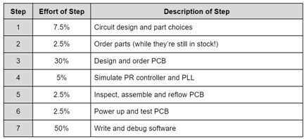
This build is broken down into a number of steps. Here is an outline of the approximate effort of each step:
Here are my previous published attempts GTI_v1, GTI_v2, GTI_v3 on instructables. It's somewhat embarrassing looking back at these because they contain countless design flaws and imperfections! These are some of the problems from GTI_v3:
- Lack of an acceptable control algorithm
- Required a transformer for isolation
- LC filter instead of a superior LCL filter
- There was no EMI filtering on the output
- There were no relays to connect and disconnect from the grid
- Measurements of voltages and current weren't that good.
- No onboard microprocessor
Let's address all these flaws!
Circuit Design and Part Choices
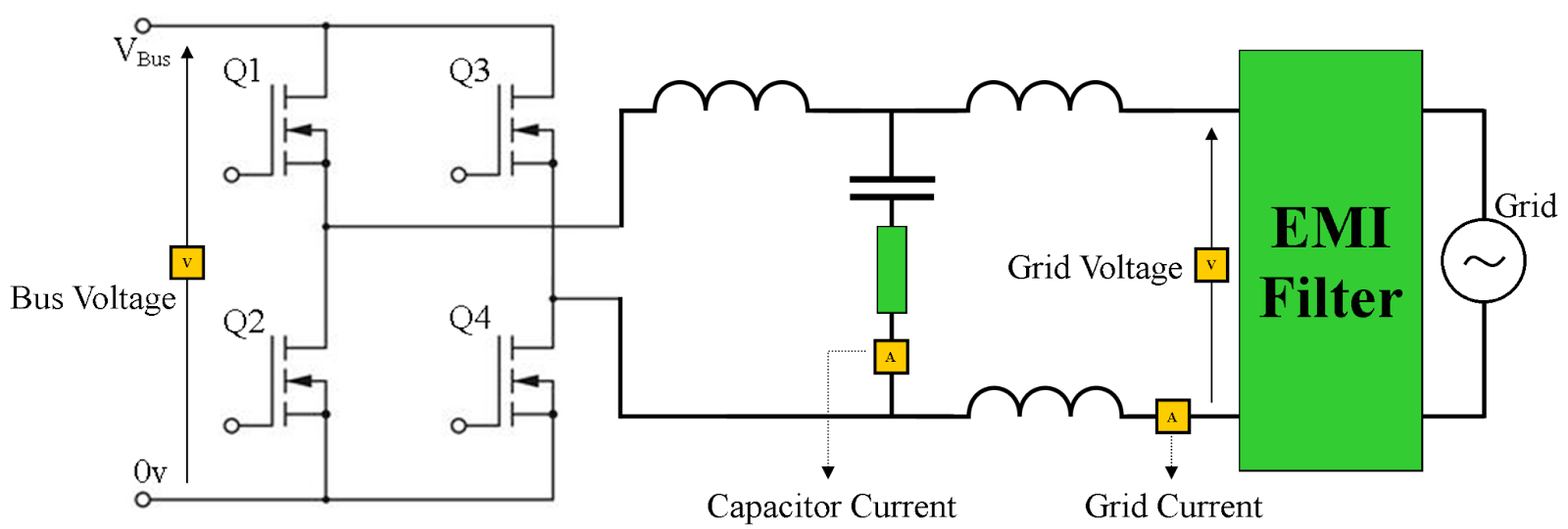
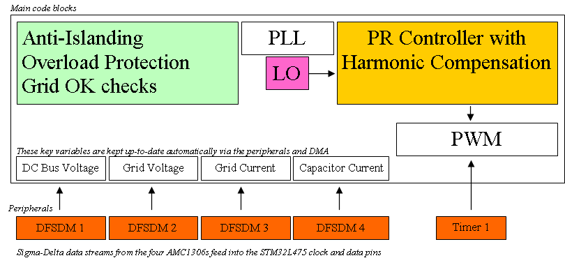
Here is the fundamental layout. In principle this is a voltage source inverter but it can be transformed into a current source inverter by running a control algorithm in a high speed microcontroller.
The controller is vital for proper functionality and needs decent measurements of bus voltage, grid voltage and grid current to work. We also measure filter capacitor current because this allows us the potential to improve performance later on.
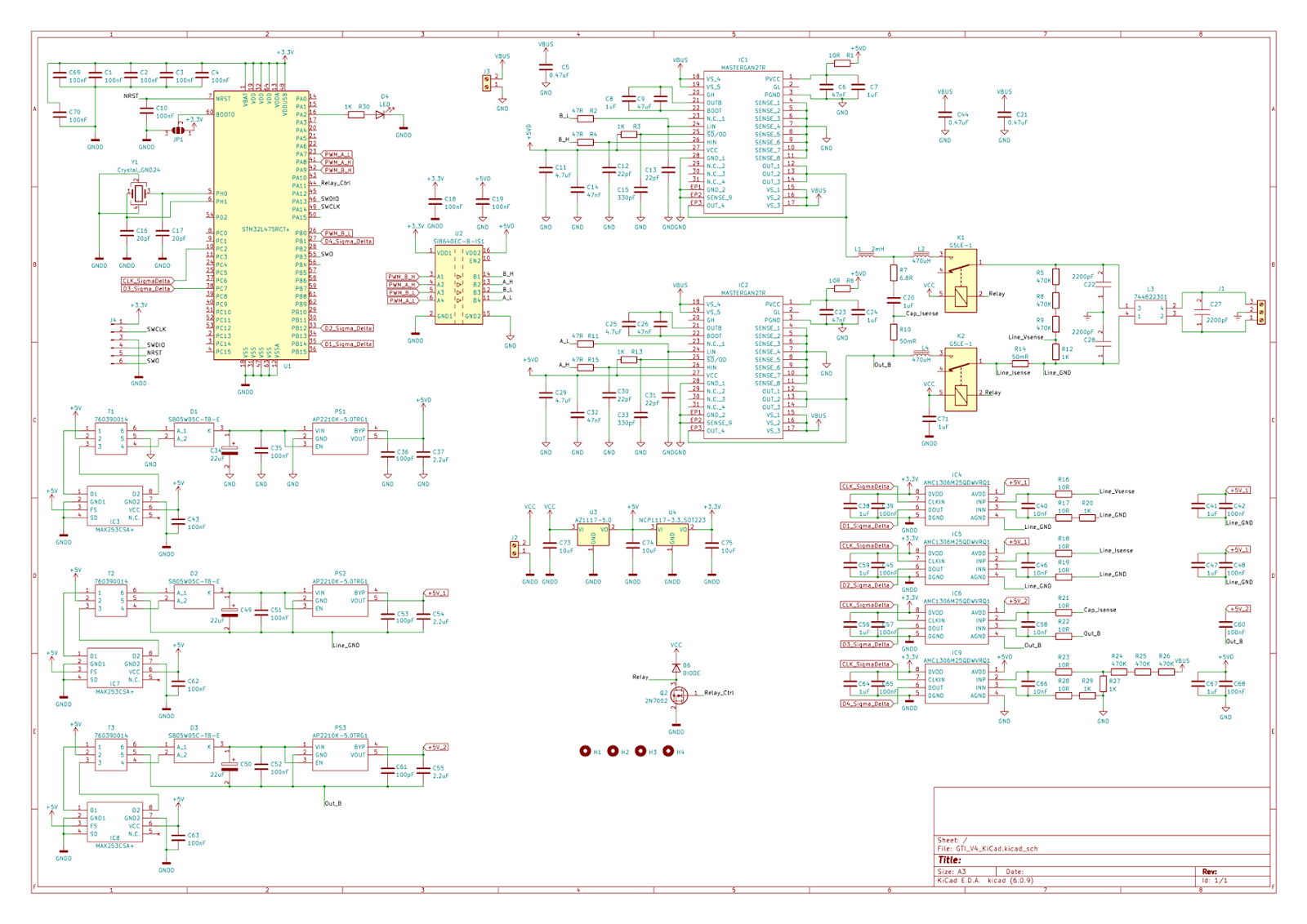
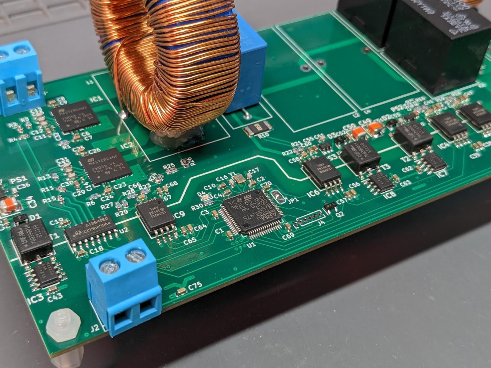
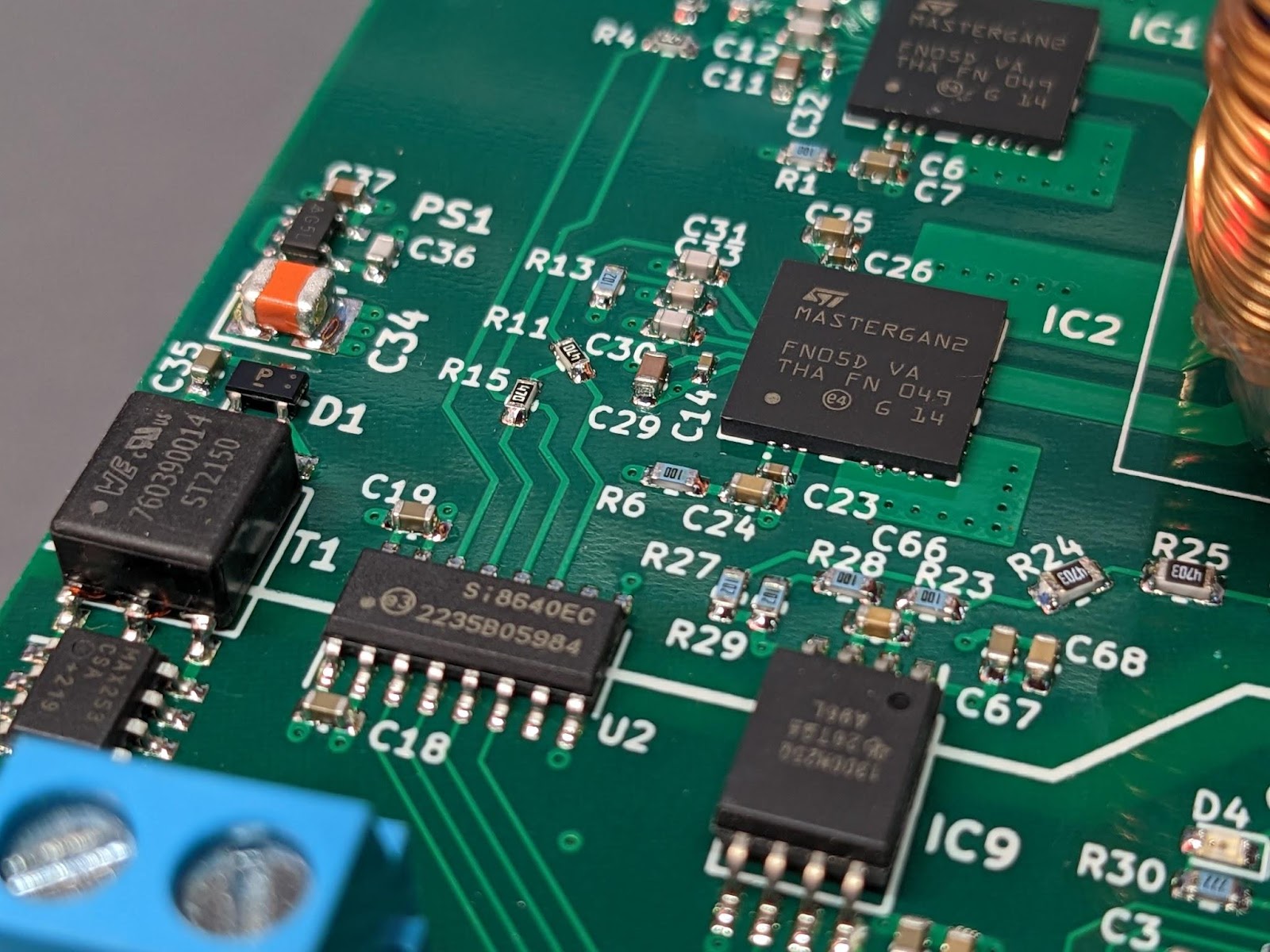
In previous versions I have built the 2 totem poles using MOSFETs and respective driver chips. In this version I’ve used a pair of MASTERGAN2s. These packages house a driver and a pair of FETs in a convenient SMD package. They are gallium nitride FETs which are pretty trendy. (In retrospect, perhaps it’d have been better to keep things simple and use off the shelf MOSFETs instead!)
An STM32L475 microcontroller is mounted on the PCB and galvanically isolated from the high voltage section of the board. We measure the 4 key analogue signals: the DC bus and grid voltages together with the grid and filter currents using AMC1306s. The STM32L475 has peripherals for receiving and processing the 4 separate sigma-delta data streams from each of the AMC1306s. This allows simultaneous isolated sampling of all important metrics. An Si8640 quad-channel digital isolator interfaces between the STM32L475 and the MASTERGAN2s.
The AMC1306 chips need isolated power supplies which are generated by mini transformers driven by MAX253 chips.
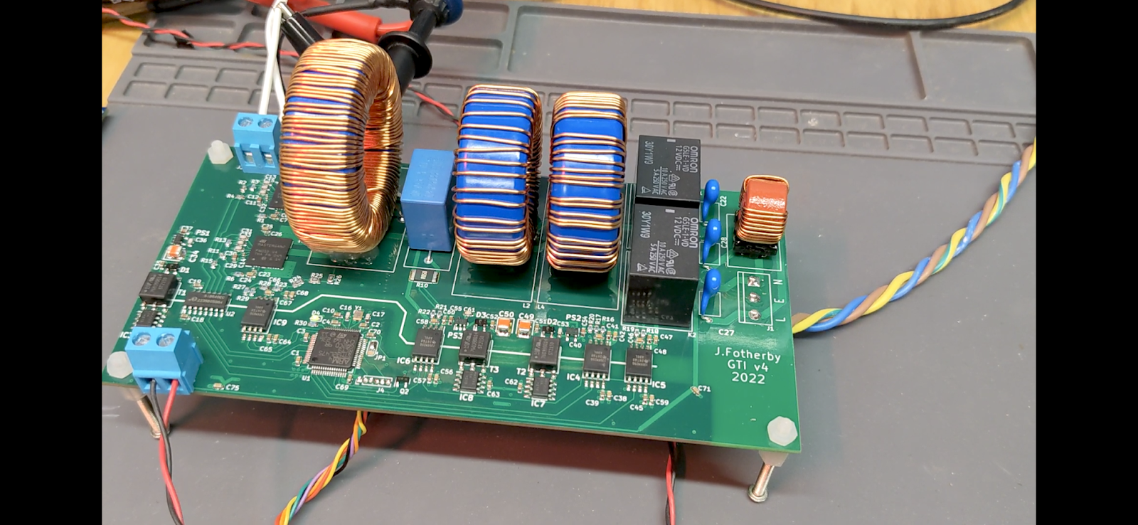
We wound the toroidal inductors to make the LCL filter. The plan is to do all high frequency switching on the top MASTERGAN2 and switch the other leg at 100 Hz to unfold the waveform. The idea being to contain all the switching noise and EMC to 1 principle area of the PCB.
The LCL filter has an inverter side inductor Li and a grid side inductor Lg. We have split the grid side inductor into 2 half sized inductors. (It was a gut feeling… this is probably unnecessary).
A robust and stable film capacitor is used for the LCL filter. In GTI_v3 X7R MLCC capacitors were used which have awful stability with changing voltage. Those capacitors were also referenced to ground which is not right for grid connected inverters.
Relays have been included to connect or disconnect from the grid. A common mode choke and some EMI filter capacitors have been added at the output. Ideally the whole PCB would be shielded within a metal enclosure too.
By following the suggested designs for each of the various chips there was very little circuit design left to do. It is very likely you could remove some capacitors and resistors but I was quite conservative as I wanted to guarantee a working design. You might note that there is no bulk capacitance other than the MLCCs and film capacitor (total ~11uF). That's because it's all off board to save on PCB area and hence cost. Here’s the BOM with links to some of the parts.
The MASTERGAN2 which is switching at only 50 Hz needed its high-side bootstrap capacitor upgraded from 1uF to 4.7uF. I have updated the design files to reflect this. The MASTERGAN2 was switching off half way through the cycle which was resolved by increasing the capacitance.
Output Filter Design
The inverter side toroidal inductor uses this core which has a permeability of 90. I wound about 125 turns for an inductance of 2mH and it has an 80% saturation current of about 3.5A. The grid side inductors used this core and they have about 53 turns creating 470uH inductors. I put in a 6.8R filter resistor and was planning to research and optimise this later on.
With grid connected applications the size of the filter capacitance is much smaller than for stand alone sine wave inverters. I understand this to be to keep the reactive current <5% of the nominal output current of the inverter.
I have made a GitHub folder of good papers within the subject of GTIs, including some on LCL filter design. Simulations help to confirm resonant frequencies and attenuations etc. I still think my filter could be better. Why are my inductors so much larger than the inductors in commercial inverters!?
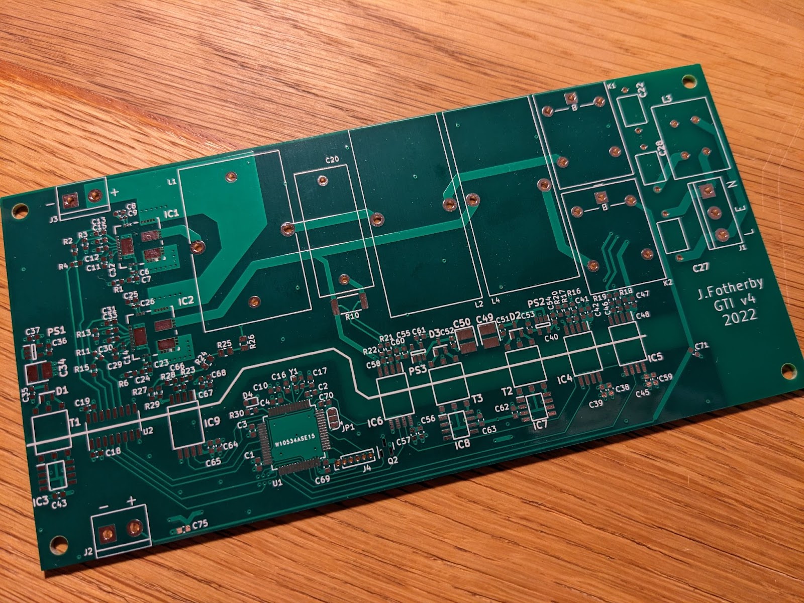
PCB Design
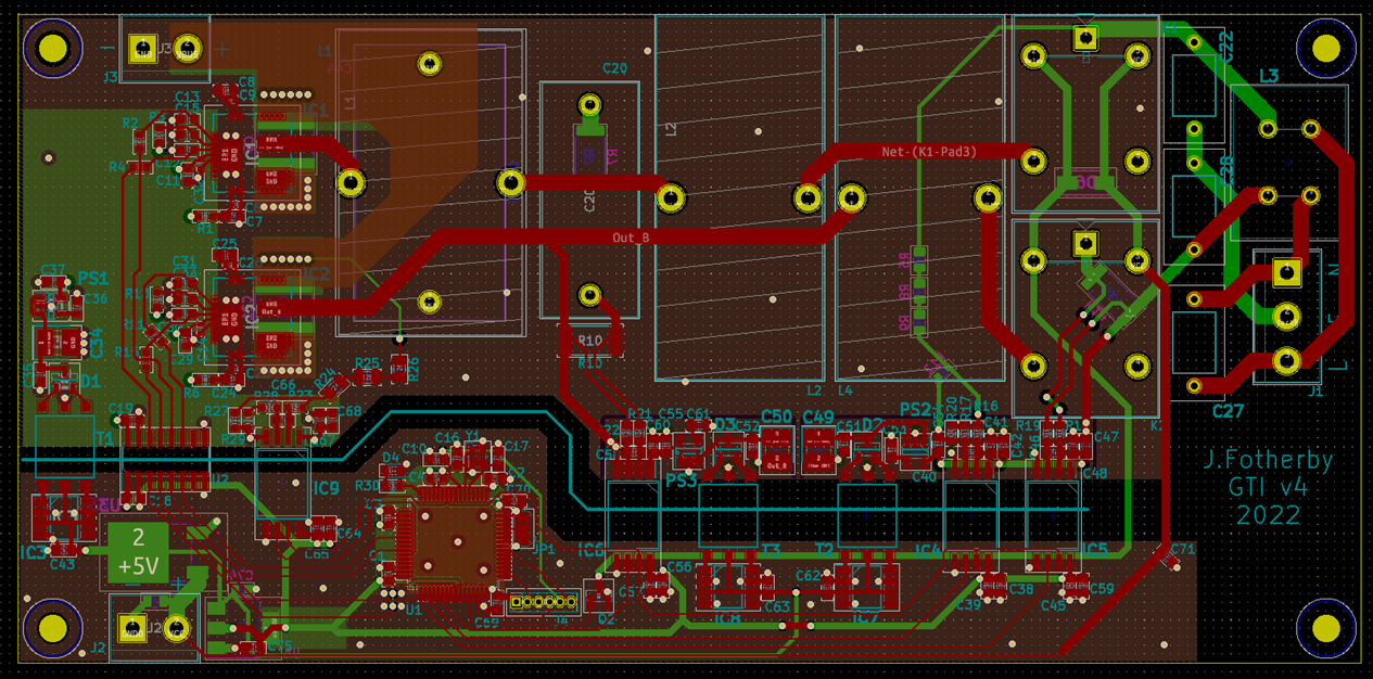
All the KiCad design files are on GitHub. The PCB design took a lot of work. In high frequency circuits the PCB layout is as important as the schematic itself. At first glance you’d be excused for thinking this is a low frequency circuit operating with modest PWM carrier frequencies of ~40kHz. However we'll be hard switching 400 V signals with nanosecond edge rates. Doing this requires frequencies hundreds of times higher than the fundamental. I’m sure we’ll have content into the 10-100MHz range. A perfect square wave is composed of a fourier series like so:

So a 400 V square wave at 40 kHz will have high frequency content eg. 40 V at 400kHz, 4 V at 4 MHz and 400 mV at 40 MHz. We don’t want those signals radiating off our PCB or contaminating our control signals.
In GTI_v2 there was such a careless approach to EMI that the 3.3V communication signals between the microcontroller and AM1306s became so corrupted that it didn’t work beyond a hundred volts! Good EMI design reflects good engineering…
I bought the book “Electromagnetic compatibility”, by Henry W. Ott. It’s a goldmine of valuable information on properly designing a PCB. Stuff like uninterrupted ground planes, how to best change layers with clock signal traces, where to place bypassing capacitors, common and differential mode chokes - these are all covered in detail in the book. He also talks about grounding and shielding. I’m sure this circuit has plenty of improvements waiting to be made but it’s a lot better than my previous versions.
PCB Stackup
I use PCBWay to manufacture my boards. They produce good quality PCBs for competitive prices with excellent turnaround times (1-2 weeks). I'd recommend them.
The PCB is a 1.6mm 4 layer board. The stackup is such that the top and bottom 2 copper layers are spaced 0.11mm apart. It took me a while to appreciate these tight spacings. I only discovered it after sawing in half and inspecting a cross section of a spare GTI_v3 PCB and then looking on PCBWays website to confirm.

These tight spacings are great for EMI though. Signals can run right on top of their respective ground plane. I’m not quite sure whether having 400V between the 2 planes would be acceptable. On searching the internet I concluded the FR4 material would not breakdown at these electric field strengths but I should look into this further.
The MASTERGAN2 are laid out the same as in the TI reference design for their evaluation board. (The pdf of this is in this folder on GitHub)
I positioned 0.22uF 450V MLCCs directly under each MASTERGAN2. Copper pour planes will provide some further capacitance for the DC Bus. There’s a 10uF DC link film capacitor mounted on the back of the PCB. A 470uF electrolytic capacitor rated to 400V is connected inline with the wires feeding the DC bus input but is’t not mounted on the PCB to save space. Altogether I think this provides adequate DC bus capacitance (~500uF).
Python PR Controller Simulation
Whilst waiting for PCBs to arrive I thought I’d run some simulations in python and implement a PR controller. I’m glad I did this because it has given me an intuition on how they work. I have learnt about and implemented a PR controller by reading the following resources:
- R. Teodorescu, 2006, “Proportional resonant controllers and filters for grid-connected voltage-source converters”
- https://imperix.com/doc/implementation/proportional-resonant-controller
Here’s how I built up the code:
Simulating a simple RL Circuit
Let’s start simple. We’ll write some python to plot the current I_m over time in an RL circuit when a voltage V is applied.

To run a simulation we iterate over small timesteps and calculate the next current value based on all the current variables:
We create 2 python files. One called model.py containing the following code:
class model:
   def __init__(self, Ts):
       self.Ts = Ts

   def BasicModel(self, I_m, V):
       # Model parameters
       Ts = self.Ts
       R=0.5
       L=0.002

       #Model
       I_m_next = V*Ts/L + I_m*(1-(R*Ts/L))
       return(I_m_next)
The second python file called Simulation.py contains this code:
import matplotlib.pyplot as plt
import numpy as np
from model import model

# Initialise Simulation parameters (use 1us timesteps, stop after 30ms)
T=0
Ts=1.0e-6
Tstop=30.0e-3
N=int(Tstop/Ts)

# Initialise Model parameters and create an instance of the model class
V=0.0
I_m=0.0
model=model(Ts)

# Initialise Plotting data
data_I_m =[]
data_V=[]
t=[]
data_I_m.append(I_m)
data_V.append(V)
t.append(0)

# Simulation
for k in range(N):
   # Set our output voltage
   V = 1.0

   # Iterate our simulated model
   I_m = model.BasicModel(I_m, V)

   # Store simulation data every 100 timesteps
   T=T+Ts
   if(k%100 == 0):
       data_I_m.append(I_m)
       data_V.append(V)
       t.append(T)

# Plotting
plt.plot(t, data_I_m, "-b", label="Measured Current")
plt.plot(t, data_V, "-r", label="Driving Voltage")
plt.legend(loc="upper left")
plt.xlabel("Seconds (s)")
plt.ylabel("Amps or Volts")
plt.grid()
plt.show()
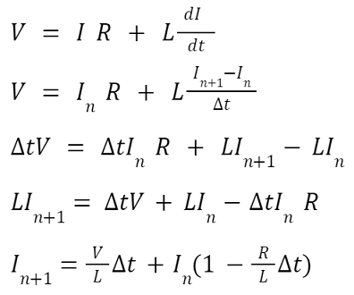
When this code runs it generates the following plot. This is exactly what you’d expect for such an RL network with R = 0.5Ω and L = 2mH.
Simulating an RL network driven by a PI controller
We want to employ a control system such that we can request a current I and leave it to the controller to adjust the driving voltage V to achieve this desired current. Ideally the requested current is obtained as quickly as possible. Let’s start with a nice simple PI controller. We add a 3rd file to our folder called controller.py containing the following code:
class controller:
   def __init__(self, kp, ki, Ts):
       self.kp = kp
       self.ki = ki
       self.Ts = Ts
       self.E_Sum = 0

   def Iterate(self, I_m, I_s):
       E = I_s - I_m
       self.E_Sum = self.E_Sum + (E * self.Ts)

       V = self.kp * E + self.ki * self.E_Sum
       return V
And we make some additions to our previous Simulation.py file so that it contains this:
import matplotlib.pyplot as plt
import numpy as np
from model import model
from controller import controller

# Initialise Simulation parameters (use 1us timesteps, stop after 30ms)
T=0
Ts=1.0e-6
Tstop=30.0e-3
N=int(Tstop/Ts)

# Initialise Model parameters and create an instance of the model class
V=0.0
I_m=0.0
model=model(Ts)

# Controller Init
I_s=0.0
kp=1.0
ki=250.0
controller=controller(kp, ki, Ts)

# Initialise Plotting data
data_I_m =[]
data_V=[]
data_I_s=[]
t=[]
data_I_m.append(I_m)
data_V.append(V)
data_I_s.append(I_s)
t.append(0)

# Simulation
for k in range(N):
   # Set our desired output current
   I_s = 1.0

   # Iterate our controller
   V = controller.Iterate(I_m, I_s)

   # Iterate our simulated model
   I_m = model.BasicModel(I_m, V)

   # Store simulation data every 100 timesteps
   T=T+Ts
   if(k%100 == 0):
       data_I_m.append(I_m)
       data_V.append(V)
       data_I_s.append(I_s)
       t.append(T)

# Plotting
plt.plot(t, data_I_m, "-b", label="Measured Current")
plt.plot(t, data_V, "-r", label="Driving Voltage")
plt.plot(t, data_I_s, "-y", label="Setpoint Current")
plt.legend(loc="lower right")
plt.xlabel("Seconds (s)")
plt.ylabel("Amps or Volts")
plt.grid()
plt.show()
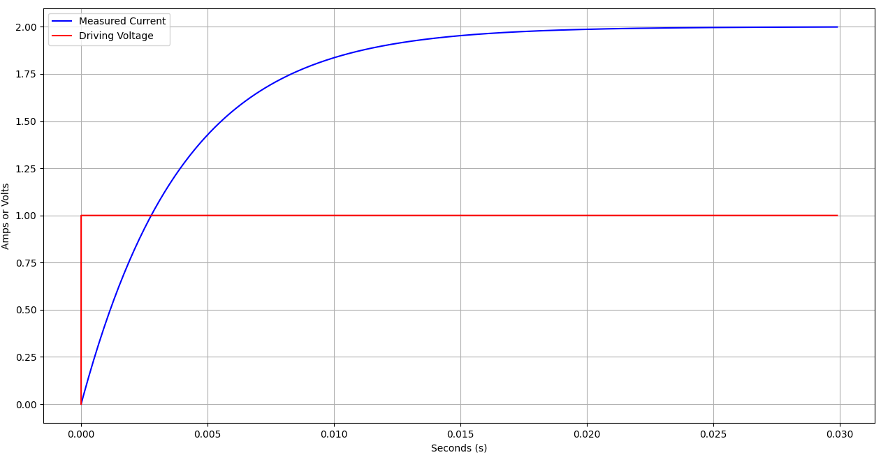
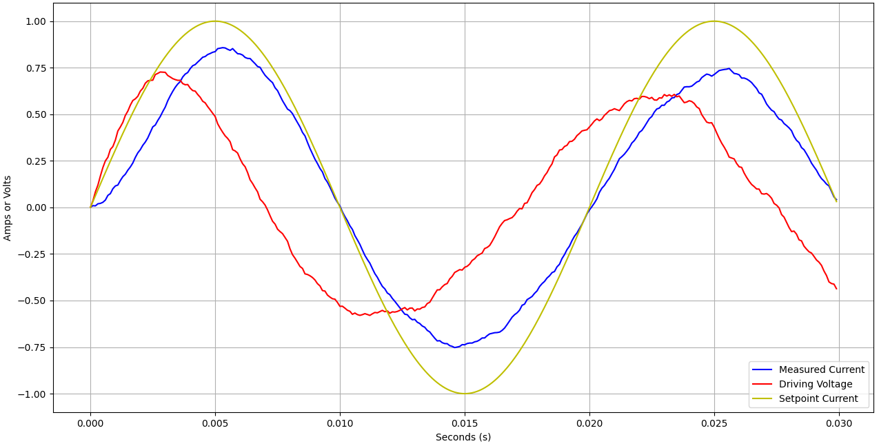
The following plot is obtained. The yellow line is the setpoint current, we set this at the start and leave it at 1 A. The controller adjusts the driving voltage V (Red) to achieve this setpoint. You can see the measured current I (Blue) reach the setpoint and stay there. The controller is tuned by adjusting 2 parameters Kp and Ki, in this plot they were set to 1 and 250 respectively.
By adjusting the tuning parameters you can reach the setpoint faster. With some combinations you get an overshoot in the measured current such as in this plot with Kp = 1.5 and Ki = 600

Using a controller is great because it abstracts you from the system you are interfacing with. You simply tell it what you want (a desired current) and it adjusts everything to achieve this. PI controllers are great for DC type circuits but when the setpoint continuously varies the controller is always playing catch up and you end up always lagging behind (i.e a phase shift).
You can increase the tuning parameters but this comes at the cost of amplifying measurement noise. Let’s adjust our code so that the current setpoint varies sinusoidally at 50 Hz.
Simulating an RL network driven by a PI controller with a sinusoidal setpoint
We simply replace:
   # Set our desired output current
   I_s = 1.0
with:
   # Set our desired output current
   I_s = np.sin(2*np.pi*50.0*T)
Additionally let’s add some gaussian distributed (white) noise into our measured current. Replace:
   # Iterate our simulated model
   I_m = model.BasicModel(I_m, V)
With
   # Iterate our simulated model
   I_m = model.BasicModel(I_m, V) + np.random.normal(0.0, 0.0006)
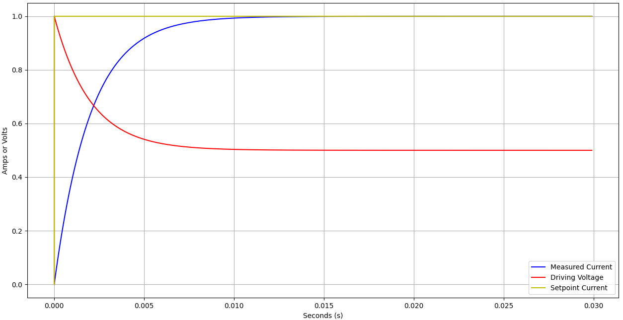
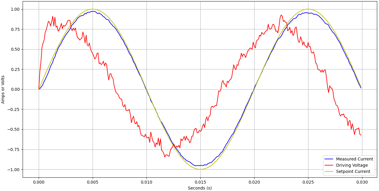
We now get this plot with with Kp = 1.5 and Ki = 600:

You can see that there is a huge lag between the measured current and the setpoint. The controller is doing a fairly rubbish job at achieving our requested current. We could increase the tuning parameters to Kp=10 and Ki=1000. This does reduce the tracking error but it massively amplifies the measurement noise into the driving voltage:
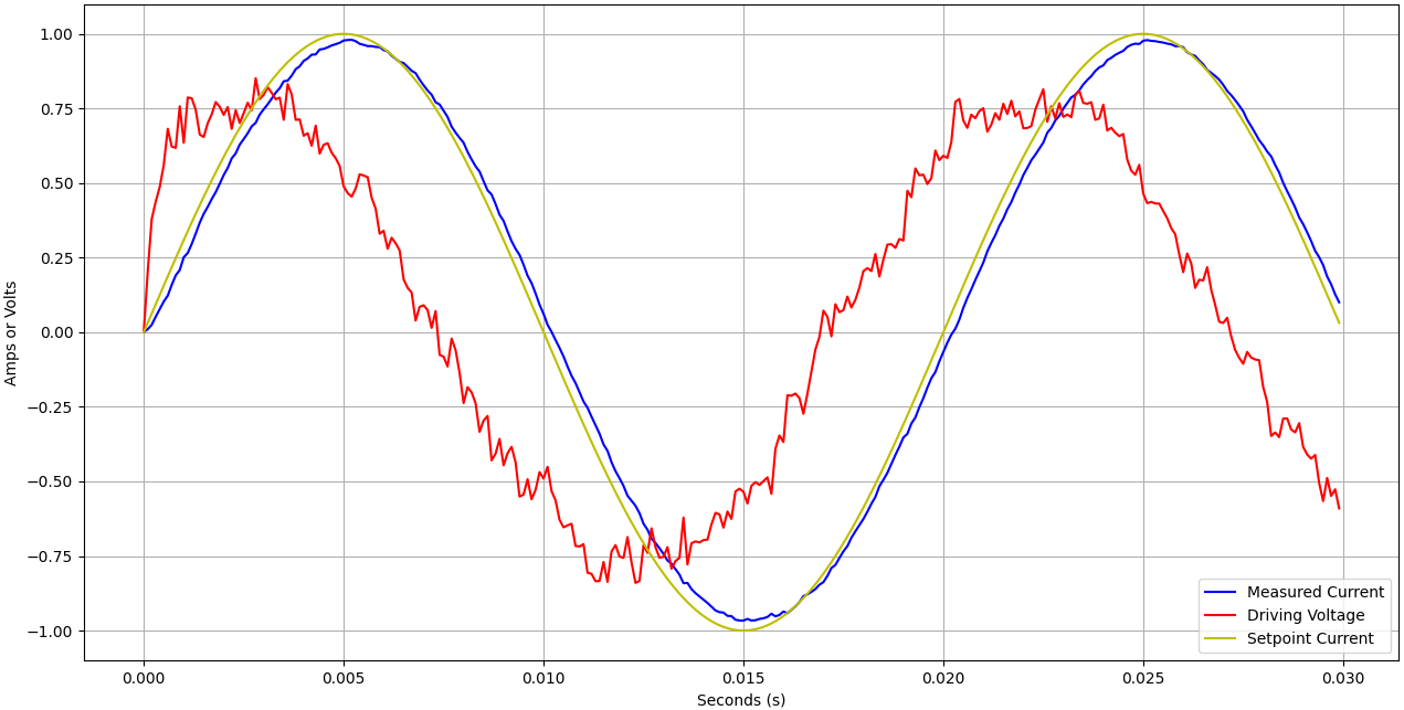
And the tracking error only gets worse with higher frequencies of the setpoint signal. Let’s implement a PR controller next. These are meant to be better because they allow you to achieve zero phase shift error around their resonant frequency. They still use a proportional term so you still get measurement noise being amplified into the driving voltage. They also need tuning right to get zero phase shift.
Simulating an RL network driven by a PR controller with a sinusoidal setpoint
Our model.py stays the same but we need to convert our PI controller to a PR controller. We replace the controller.py code with
class controller:
   def __init__(self, kp, kr, wres, wdamp, Ts):
       self.kp = kp
       self.Ts = Ts
       self.kt = 2/Ts

       self.a1 = 2 * kr * self.kt * wdamp
       self.b0 = self.kt * self.kt + 2 * self.kt * wdamp + wres * wres
       self.b1 = 2 * self.kt * self.kt - 2 * wres * wres
       self.b2 = self.kt * self.kt + 2 * self.kt * wdamp + wres * wres

       self.E_Prev1=0
       self.E_Prev2=0
       self.U_Prev1=0
       self.U_Prev2=0

   def Iterate(self, I_m, I_s):
       E = I_s - I_m

       Ua = self.a1 * self.E_Prev1 - self.a1 * self.E_Prev2
       Ub = self.b1 * self.U_Prev1 - self.b2 * self.U_Prev2
       Ui = (Ua + Ub) / self.b0

       self.E_Prev2 = self.E_Prev1
       self.E_Prev1 = E
       self.U_Prev2 = self.U_Prev1
       self.U_Prev1 = Ui

       V = (self.kp) * E + Ui
       return V
We only need to make a couple changes to our Simulation.py file:
From:
# Controller Init
I_s=0.0
kp=1.0
ki=250.0
controller=controller(kp, ki, Ts)
To:
# Controller Init
I_s=0.0
kp=1.5
kr=10000.0
Wres_50 = 2.0 * np.pi * 50.0
Wdamp_50 = 2.0 * np.pi * 0.01
controller=controller(kp, kr, Wres_50, Wdamp_50,  Ts)
With these tuning parameters we get a zero steady state phase error as shown in this plot:
The tuning parameters are too weak here because the amplitude is quite reduced from the setpoint. By adjusting Kp = 8.0 and Kr = 100,000 we get far better tracking. You could easily filter the high frequency measurement noise if desired.
So PR controllers appear to be an improvement over PI controllers. There are many different control algorithms available and the biggest competitor is probably PI control within a DQ rotating reference frame. Some especially interesting algorithms include dead-beat control and model predictive control (MPC). Here’s a paper summarising all of the various control algorithms. Here’s an interesting write-up on an MPC controller simulated by a university student.
RL network with grid voltage driven by a PI controller with a sinusoidal setpoint
So far we haven’t included the grid voltage in our model. The grid voltage of course plays quite a significant role. Let’s adjust our model to be like so:

The grid voltage should be a 50 Hz sine wave however the grid voltage is quite dirty in reality. It contains harmonics at 150, 250, 350, 450 Hz and beyond together with spikes and surges etc.
We make a few minor tweaks to our model.py file to include this:
class model:
   def __init__(self, Ts):
       self.Ts = Ts

   def BasicModel(self, I_m, V, Vgrid):
       # Model parameters
       Ts = self.Ts
       R=0.5
       L=0.002

       #Model
       I_m_next = (V-Vgrid)*Ts/L + I_m*(1-(R*Ts/L))
       return(I_m_next)
And here is the Simulation.py code with a few small changes and tuning adjustments incorporating a 50Hz fundamental grid voltage in addition to a 150 Hz harmonic:
import matplotlib.pyplot as plt
import numpy as np
from model import model
from controller import controller

# Initialise Simulation parameters (use 1us timesteps, stop after 30ms)
T=0
Ts=1.0e-6
Tstop=60.0e-3
N=int(Tstop/Ts)

# Initialise Model parameters and create an instance of the model class
V=0.0
I_m=0.0
Vgrid=0.0
model=model(Ts)

# Controller Init
I_s=0.0
kp=2.0
kr=10000.0
Wres_50 = 2.0 * np.pi * 50.0
Wdamp_50 = 2.0 * np.pi * 0.001
controller=controller(kp, kr, Wres_50, Wdamp_50,  Ts)

# Initialise Plotting data
data_I_m =[]
data_V=[]
data_I_s=[]
data_Vgrid=[]
t=[]
data_I_m.append(I_m)
data_V.append(V)
data_I_s.append(I_s)
data_Vgrid.append(Vgrid)
t.append(0)

######################################################################################
# Simulation
for k in range(N):
   # Set the Grid voltage
   Vgrid = 1 * np.sin(2 * np.pi * 50.0 * T) + \
           0.15 * np.sin(2 * np.pi * 150.0 * T + 0.0)

   # Set our desired output current
   I_s = np.sin(2*np.pi*50.0*T)

   # Iterate our controller
   V = controller.Iterate(I_m, I_s)

   # Iterate our simulated model
   I_m = model.BasicModel(I_m, V, Vgrid) + np.random.normal(0.0, 0.0006)

   # Store simulation data every 100 timesteps
   T=T+Ts
   if(k%100 == 0):
       data_I_m.append(I_m)
       data_V.append(V)
       data_I_s.append(I_s)
       data_Vgrid.append(Vgrid)
       t.append(T)

# Plotting
plt.plot(t, data_I_m, "-b", label="Measured Current")
plt.plot(t, data_V, "-r", label="Driving Voltage")
plt.plot(t, data_I_s, "-y", label="Setpoint Current")
plt.plot(t, data_Vgrid, "-g", label="Grid Voltage")
plt.legend(loc="lower right")
plt.xlabel("Seconds (s)")
plt.ylabel("Amps or Volts")
plt.grid()
plt.show()
Running all this generates the following plot. You can see the green trace is our grid voltage containing some 150Hz harmonic content. Because our PR controller has a resonant frequency at 50Hz the resonant term does nothing to cancel this frequency. As such you see the measured current (blue) is distorted because it has 150 Hz content too.
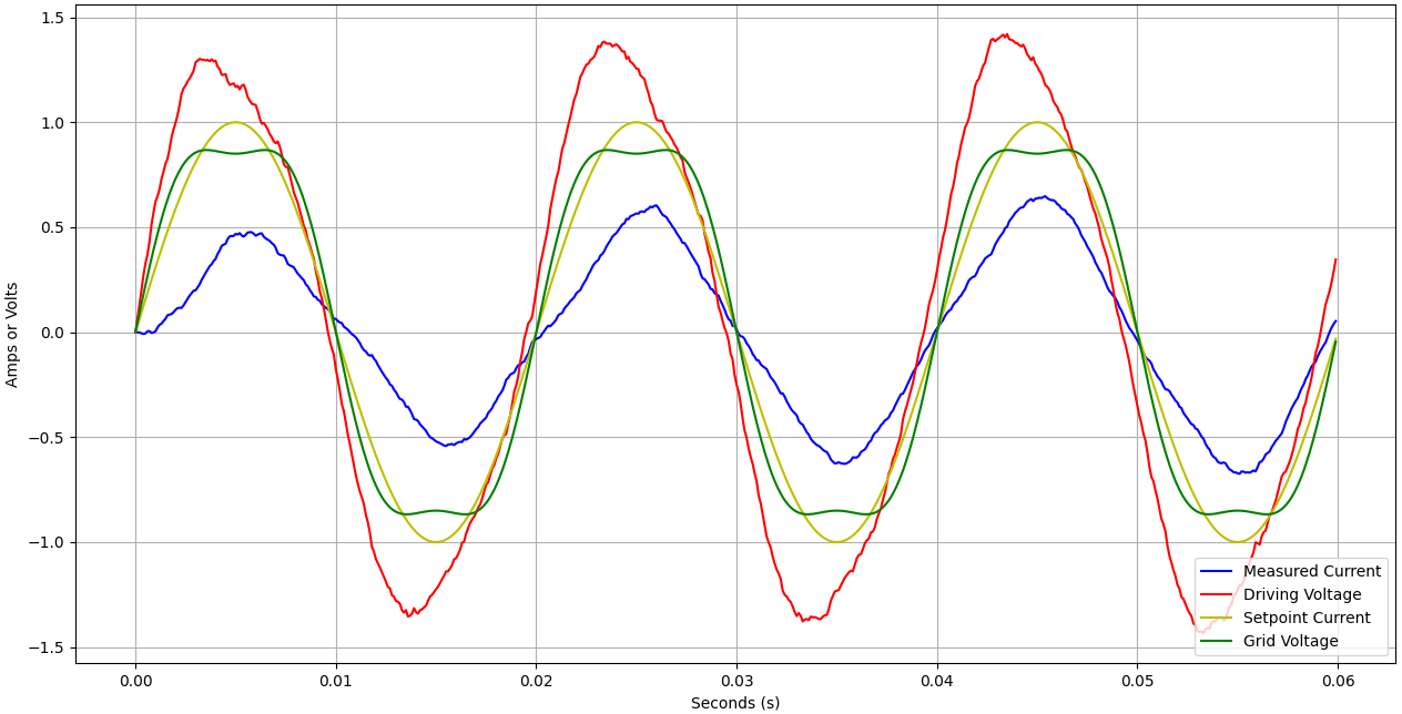
This is bad. We requested a 50 Hz clean sinusoidal output current but are getting distortions and harmonic content leaking through. An inverter using this may fail regulatory approval on grounds of harmonic distortion.
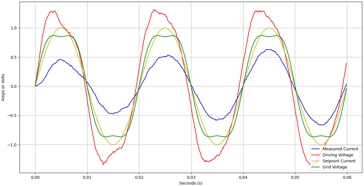
To improve this issue we can create another instance of our PR controller and run the two in parallel. The second PR controller can have a resonant frequency centred on the 150 Hz harmonic:
We call our PR controller instances controller50 and controller150. The former is the only one with any Kp gain:
# Controller Init
I_s=0.0
kp=2.0
kr=10000.0
Wres_50 = 2.0 * np.pi * 50.0
Wdamp_50 = 2.0 * np.pi * 0.001
controller50=controller(kp, kr, Wres_50, Wdamp_50, Ts)

kr=100000.0
Wres_150 = 2.0 * np.pi * 150.0
Wdamp_150 = 2.0 * np.pi * 0.001
controller150=controller(0, kr, Wres_150, Wdamp_150, Ts)

We also add the controller150 into our main simulation for loop
# Iterate our controller
V = controller50.Iterate(I_m, I_s) + controller150.Iterate(I_m, I_s)
This results in the following plot which is arguably quite a bit better. The above method is called harmonic compensation. Several compensators can be used, each working at the major harmonics.
I didn’t optimise the tuning parameters in these simulations. I just wanted to get the point across. Here’s a paper called Tuning Rules for Proportional Resonant Controllers. With the right tunings you can get pretty good tracking.
PR controllers have a given bandwidth which means they take time to respond and in some of the plots above you can see the measured current waveform evolving cycle to cycle following start-up. I think this is more pronounced with poor tuning settings.
Python PLL Simulation
The Phase-Locked Loop (PLL) is a vital part of a grid tie inverter. Its job is to synchronise our local oscillator (LO) with that of the grid’s phase and frequency. We run a LO in software by either stepping through a cosine lookup table or by using math.h to directly calculate cosine() values based on an incrementing index (ie Phase). The microprocessor is clocked from a crystal oscillator so we can accurately synthesise a perfect 50 Hz cosine.
We need a LO because it’ll be used as the setpoint reference for our output current controller (independent of whether that controller is a PI, PR, D/Q, dead-beat, MPO). We must output a current waveform that is in phase and frequency (i.e. grid tied) with the grid. Therefore we need our LO adjusted continuously so it has exactly the same phase (and therefore frequency) to the grid waveform (i.e phase locked). The way we make these adjustments is via a PLL.

The grid signal provides our reference waveform and will include noise and harmonic content. When the program starts our LO will initially be a pure 50 Hz cosine with an arbitrary phase. It'll need some prompt adjustment!
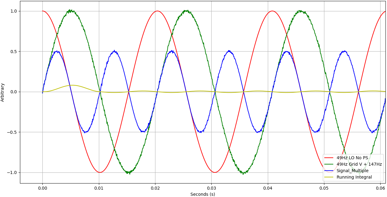
Let’s talk through the maths of our phase detector. The job of which is to measure the phase difference between the 50 Hz grid fundamental and LO signal. We start by simply multiplying the 2 signals:

Looking at this graphically, VG in green is our 50 Hz grid signal. VLO in red is our 50 Hz LO with a 30 degree phase error. The resulting multiple is in blue showing a 100 Hz signal riding on a DC bias.
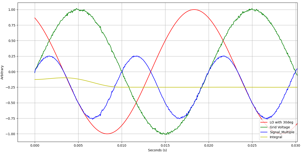
Before we talk about the yellow line we realise that in normal operation: Wg = WL which simplifies the maths to:
Next we maintain a running integral of this multiplication over the last period (20ms for a 50 Hz signal). In doing this we obtain the yellow line. Note at startup the running integral is not yet “filled” so there’s some brief disturbance. What’s nice about this is that integrals of periodic functions over a period are equal to zero so:
This is great. It means that the result of our running integral is a measure of the phase difference between the grid and our local oscillator. We can use this as the error signal for a PI controller. If the phase difference is ever non zero the frequency of our LO is adjusted to return the difference to zero.
This is the python code we used for these simulations:
import matplotlib.pyplot as plt
import numpy as np

Samples_per_Period = 400
Periods_to_plot = 4
Samples=Samples_per_Period*Periods_to_plot
Time_of_simulation = 0.02*Periods_to_plot

t = np.linspace(0, Time_of_simulation, Samples)

# Simulate a typical Grid voltage waveform
Vgrid = 1 * np.sin(2 * np.pi * 50 * t) + \
       0.1 * np.sin(2 * np.pi * 150 * t + 0.1) + \
       np.random.normal(0.0, 0.01, Samples)

# Our LO is a pure cosine as it is created in software
LO = np.cos(2 * np.pi * 50 * t - 10*np.pi/180)

# Multiply our Grid voltage with our LO
Signal_Multiple = Vgrid * LO

# Keep a running integral over the last period (Same a convolution)
window = np.ones(Samples_per_Period)/Samples_per_Period
Integral = np.convolve(Signal_Multiple, window, 'same')

# Plotting
plt.plot(t, LO, "-r", label="LO")
plt.plot(t, Vgrid, "-g", label="Grid V")
plt.plot(t, Signal_Multiple, "-b", label="Signal_Multiple")
plt.plot(t, Integral, "-y", label="Running Integral")
plt.legend(loc="lower right")
plt.xlabel("Seconds (s)")
plt.ylabel("Arbitrary")
plt.grid()
plt.show()
Imperfections in our PLL
The grid frequency only varies about 50 Hz by +/-0.5 Hz. In the worst case scenario our PLL could be 0.5 Hz wrong at startup. If the grid and LO frequency are mismatched by 0.5 Hz then a phase error will gradually accumulate. Since the result of our integral is sin() our error signal will slowly vary like so:

At the zero-crossing points the curve is nice and linear with a maximal gradient. This is good since it means small phase shifts result in a quickly changing error signal. There will also be stable and unstable equilibrium points. At 1 second, the phase error between the (nearly equal frequency) signals has accumulated to 180 degrees. You can’t get a bigger phase error than 180 but our error signal is actually zero! It’s not a problem because in reality we’d never let our phase error get more than a few degrees.
Say for example at system start-up there was a perfect 180 degree phase error between our grid and LO signals. Our phase detector would output a zero error so we wouldn’t initially adjust our LO frequency. However we are at an unstable equilibrium point and any slight deviation in phase will result in positive feedback. We’ll then either decrease our LO frequency to bring the phase error to 0 degrees. Or alternatively depending on which way the cookie crumbles we’ll increase our LO frequency until the phase error is +360 degrees (which is equivalent!).
A few further points
- Harmonic content in the grid waveform doesn’t affect the error signal at all. This is because we are integrating over multiples of a period which always equal zero.
- There is minimal noise in the integrated signal because integrals are effective low pass filters.
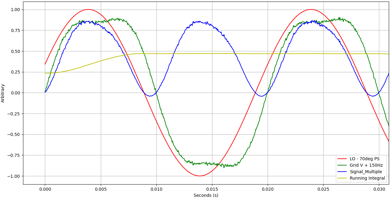
- If we don’t integrate over exactly a period. Say we always integrate over 20 ms but our grid and LO are both running at 50.2 Hz - then we’ll get a very small amount of signal_multiple leaking through into our error signal. The following plot is with our grid and LO at 49 Hz (The grid would never deviate this far). You can see some 98 Hz leaking through but it’s clearly nothing to worry about.
Enough with python simulations! They have been key to building up some intuition but we need to start implementing all this in real time on actual hardware with real world signals.
PCB Assembly

The PCB boards have arrived. To assemble the PCB I applied solder paste using a stainless steel stencil before mounting the components and reflowing in a cheap toaster oven. It took a morning.
The parts reflowed beautifully. I used this Mesh 4 Sn63Pb37 solder paste
Once assembled I cautiously powdered up the logic section of the board. It pulled 80 mA. The mini transformers were all working nominally and every section was getting the appropriate supply voltage - Win!
Software Development
I chose to use the STM32L475 microcontroller because it had four digital filters for sigma delta modulators. It was also in stock! I had a 10-point plan for the software development:
- Make a new project, blink the onboard LED and toggle the relays
- Set up timer 1 to output a fixed duty PWM to drive the MASTERGAN2s
- Set up the DFSDM peripherals to read the AMC1306s and write values to main memory via DMA
- Modulate the PWM duty with a 50 Hz LO to create a voltage source inverter
- Build our overload protection system
- Test thermal performance and efficiency of the circuit driving a resistive load
- Build our PR controller and test it driving a current through an RL load
- Build our PLL and ensure it’s synchronising with the grid voltage
- Put it all together! Push power into the grid
- Celebrate!
Upload a Blink Sketch
Blinking an LED is a good milestone because it means you’ve set up your development environment, connected to the target and uploaded some code. It confirms that the microcontroller is powered properly by the PCB and is operating correctly.
12V was applied to the logic section and the programming header was connected to the SWD port of a STM32F412 Dev board. We can use ST-Link to upload code.
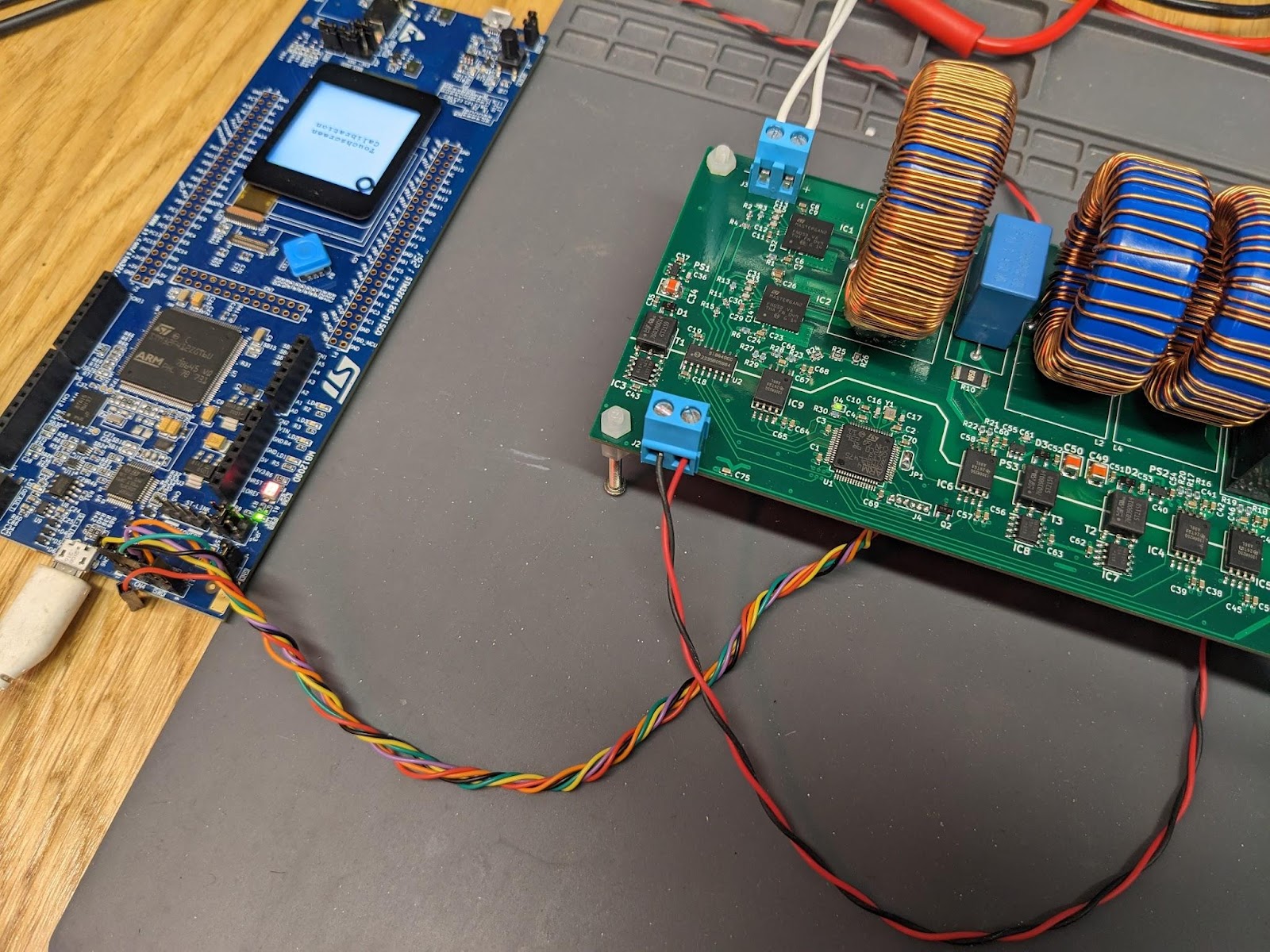
STM32CubeIDE was used to write the software. It’s free and incorporates STM32CubeMX. This latter piece of software provides a graphical interface to configure the clock settings and all the peripherals. It's incredibly helpful and saves an enormous amount of effort. (On niche stuff it can have the odd bug)
A 16 MHz crystal is mounted on the PCB and STM32CubeMX can calculate all the PLL settings to give you the system clock speed you want. In this case we'll max out the clock speed at 80 MHz. Here are the clock settings on CubeMX:

CubeMX makes it a piece of cake to choose various pins and register them with the peripheral you want. We configure the LED Pin (PA2) and relay pin (PA11) as an output and with a click of a button all the code is done for you.
Here's the only code we've had to write so far:
	HAL_GPIO_WritePin(GPIOA, LED_Pin, GPIO_PIN_SET);
	HAL_Delay(50);
	HAL_GPIO_WritePin(GPIOA, LED_Pin, GPIO_PIN_RESET);
	HAL_Delay(50);
This goes in the main loop between the /* USER CODE BEGIN 3 */ and /* USER CODE END 3 */ statements. The code uploaded and ran on the first attempt which was a huge relief!
Setup timer 1 to output a fixed duty PWM
Again, using CubeMX makes setting up timer 1 a doddle. We want PWM mode with complementary outputs on channel 1 and 2. We use these settings to create a 40 kHz PWM signal with a PWM duty between 0-1000 and a deadtime of 25ns:
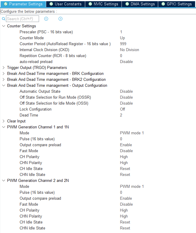

You can calculate the deadtime as follows: Timer clocked at 80 MHz, Internal clock division set = “No Division”, Deadtime = 2 which equates to 2 periods of the timer clock = 25ns.
A duty cycle between 0-1000 and PWM frequency of 40kHz means our pulse width increments in steps of 25ns. The MASTERGAN2 datasheet suggests a minimum pulse width of 120ns to avoid distorted output waveforms. We can tolerate a degree of distortion, I doubt it'll be significant because we will rarely be operating with such small duties.
We have to add a few lines of code into our main.c file to start the timers on both the regular and complementary outputs:
HAL_TIM_PWM_Start(&htim1, TIM_CHANNEL_1);
HAL_TIMEx_PWMN_Start(&htim1, TIM_CHANNEL_1);
HAL_TIM_PWM_Start(&htim1, TIM_CHANNEL_2);
HAL_TIMEx_PWMN_Start(&htim1, TIM_CHANNEL_2);
We can set the duty to 50% (500/1000) by directly writing to the CCR registers. We'll keep the bottom GaN (Channel 1) low and only switch on the top GaN (Channel 2 - which directly feeds into the inverter inductor):
htim1.Instance->CCR1 = 0;
htim1.Instance->CCR2 = 500;
The switching node voltage was measured on a Picoscope 4224A with a 15V bus voltage. We can see beautiful sharp edges. The deadtime was reduced to 25ns based on these waveforms. With longer deadtimes the dead-zone was clearly visible but at 25ns it had just disappeared.
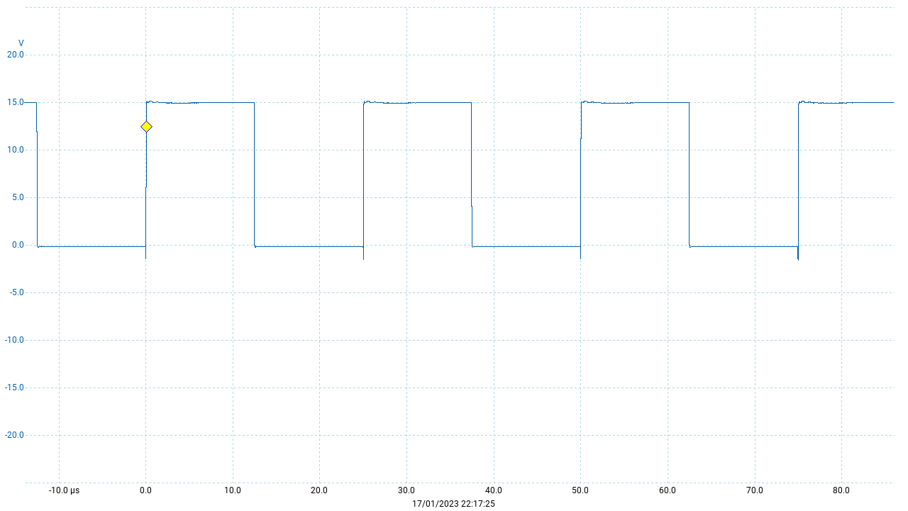
The inverter's output was connected to a 6 ohm power resistor and a few input and output measurements were taken using a multimeter (quoted accuracies) with a 20% applied duty cycle:
- DC Bus input voltage = 14.99 V (+/- 0.5%)
- DC Bus input current = 81.8 mA (+/- 1%)
- Inverter output voltage = 2.54 V (+/- 0.5%)
- Inverter output current = 420 mA (+/- 1%)
These measurements show an 87% efficiency. At 1st glance that seems rubbish but it was entirely expected for these low operating voltages. The reason is that this inverter is designed for DC bus voltages of 380 V.
Let’s measure the inverters output resistance. We set the duty to 0% so both GaNs are switched to GND continuously. We can then apply a current through the output and measure the voltage drop. This current must travel through all the inductors, PCB traces and through both GaN low-side drain-source resistances. It is an excellent measurement of the inverter’s DC output impedance.

This created a plot from which linear regression provides us with a value of 0.95 ohms.
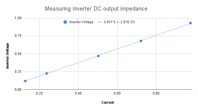
It now makes complete sense why we only measured 87% efficiency. 0.95 ohms is large compared to the 6 ohm load we were driving. Hence for a given current, 6/6.95 of the input power will enter the load and 0.95/6.95 will be dissipated by the inverter’s internal impedance. Note that 6/6.95 = 86% which is very close to our measured 87% efficiency. All good so far.
Set up the DFSDM peripheral
The STM32L475 has 4 onboard filters for processing PDM bitstreams. We can therefore dedicate a filter to each AMC1306. CubeMX makes lightwork of the configuration:
- Configure the DFSDM clock. A divider of 8 gives a clock speed of 10MHz. We set CKOUT because we want the STM32L475 to output this clock signal to all AMC1306s.
- Configure which channel is connected to which input pin and use the internal clock.
- Channel config: SPI with rising edge, no offset, no bit shifting
- Set the GPIO pins for maximum output speed
- Configure each filter: Set which filter is fed by which channel. Set for continuous mode. Set for Sinc3 with Fosr=125 and Iosr=4.
- Configure the DMA for peripheral-to-memory with a circular buffer
Only 1 line is required in our main.c file to start each filter:
	HAL_DFSDM_FilterRegularStart_DMA(&hdfsdm1_filter0, Vbus_DMA, 1);
	HAL_DFSDM_FilterRegularStart_DMA(&hdfsdm1_filter1, Igrid_DMA, 1);
	HAL_DFSDM_FilterRegularStart_DMA(&hdfsdm1_filter2, Vgrid_DMA, 1);
	HAL_DFSDM_FilterRegularStart_DMA(&hdfsdm1_filter3, Icap_DMA, 1);
A 10 MHz DFSDM clock is suitable to feed the AMC1306’s which can accept clocks between 5-20 MHz. The AMC1306 datasheet advises a Sinc3 filter. Here’s A fantastic resource explaining sigma-delta modulation and the config settings. I set Fosr=125 and Iosr=4. The data will have a dynamic range of +/- For^3 x Iosr = +/- 7812500. The data rate will be 10MHz/(Fosr*Iosr) = 20khz. This is an awesome amount of resolution. The values are automatically written to main memory by the DMA. (Note. the data is present in the most significant 24-bits of the 32-bit word)
I calibrated the readings by taking various measurements and plotting graphs of best fit again. Each time the DMA completes a conversion the respective result is converted to a floating point value in SI units. The IDE has a debug mode so it’s easy to read off the values the microprocessor is acquiring.
Modulate the PWM duty with 50 Hz LO
Creating a LO is easy. We configure a timer to call a function at 3.2 KHz. Each time the function is called we increment our phase index. Our phase therefore increments through 64 steps every 50 Hz period.
When the LO value is wanted we'll simply put this index through a sine or cosine function to get the respective sample. Here are is the code for our timer ISR:
void HAL_TIM_PeriodElapsedCallback(TIM_HandleTypeDef *htim) {
if (htim == &htim4)
{
	TIM4->ARR = SINE_STEP_PERIOD;
    _50_Index += 1;

    if(_50_Index == SINE_STEPS)	 {
      _50_Index = 0;
    }
}
We can easily adjust the LO frequency by adjusting the overflow value (SINE_STEP_PERIOD) of the timer. We only ever want to adjust it about 50Hz by about +/-0.5Hz so it’s a fairly proportional relationship between counter overflow value and frequency.
We configure a second timer to run a periodic function at ~13 kHz. Each time this function runs it gets the LO sine value and writes to our duty. This modulates our duty cycle with a 50 Hz sine wave. We improve our resolution beyond 64-steps by performing some interpolation.
#define	DUTY_LIMIT 1000

if (htim == &htim3)
{
  static int16_t Duty_Cycle;

  // Interpolate our LO steps to get a more accurate LO sample:
  uint32_t Timer4_CNT = TIM4->CNT;
  uint8_t Lookup_Index = _50_Index;
  float diff = Sin_LookupF[Lookup_Index + 1] - Sin_LookupF[Lookup_Index];
  float Timer4_CNT_Ratio = 0.001f * (float)Timer4_CNT;
  float LO_Sample_256 = Sin_LookupF[Lookup_Index] + diff * Timer4_CNT_Ratio;

  // Constrain and output the new duty cycle
  Duty_Cycle = (int16_t)(LO_Sample_256 * 3.8);
  Duty_Cycle = CONSTRAIN(Duty_Cycle, -DUTY_LIMIT, DUTY_LIMIT);

  if(Duty_Cycle >= 0) {
    htim1.Instance->CCR1 = 0;
    htim1.Instance->CCR2 = Duty_Cycle;
  }
  else {
    htim1.Instance->CCR1 = 1000;
    htim1.Instance->CCR2 = 1000 + Duty_Cycle;
  }
}
This makes Channel 1 switch between V_Bus and GND every half cycle. All the high frequency PWM is done on channel 2 which directly feeds the inverter inductor.
With the 6 ohm shunt resistor on the output we can now see a stunning 50 Hz signal across it (in red using a 50x differential probe):
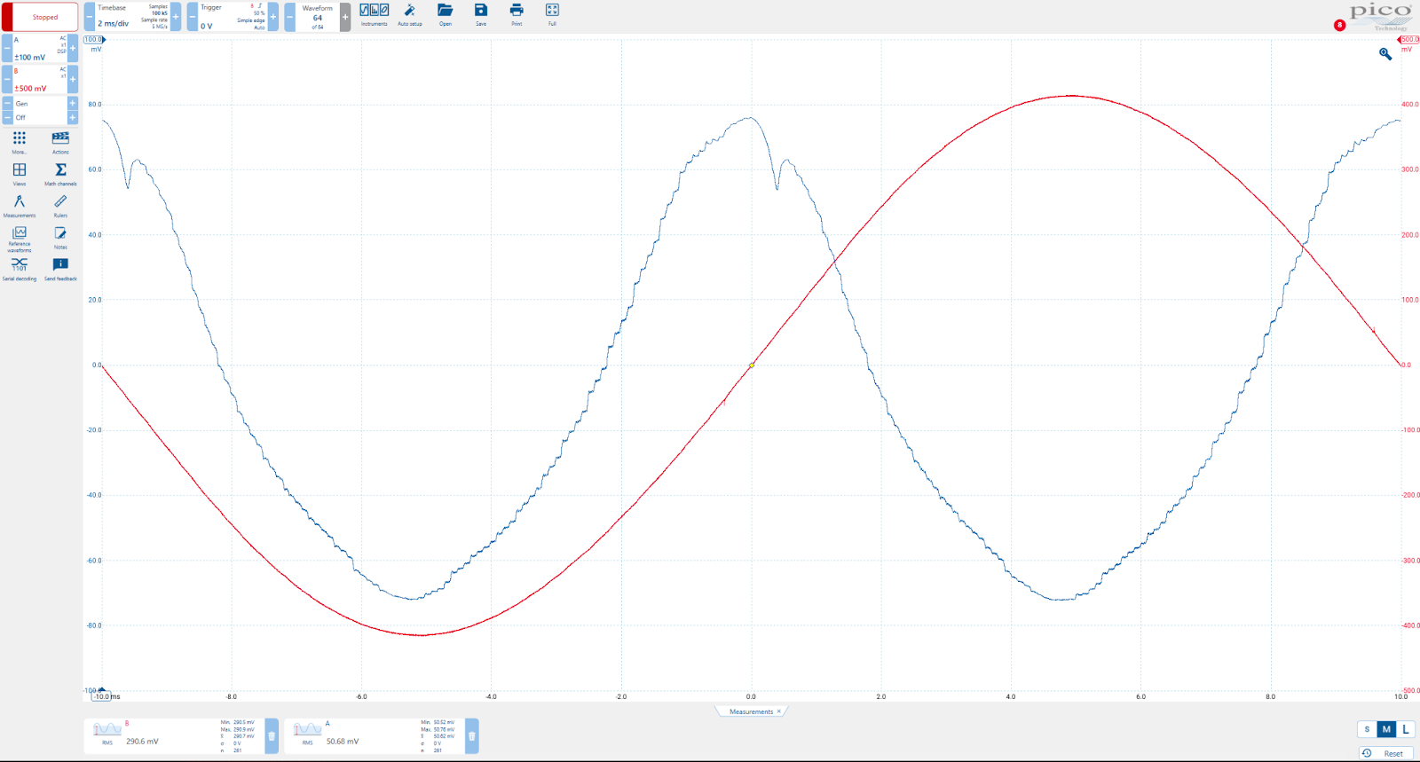
The DC bus was given 25 V and our PWM duty was modulated by a sine wave to swing to +/-97%. The picoscope measured an RMS voltage of 14.53 V across the 6 ohm load which implies an RMS current of 2.42 A. The GaNs were only warm to touch at about 25 degrees celsius above ambient.
Also superimposed on this view is the AC component of the DC bus voltage. You can see how this waveform is twice the frequency of the 50 Hz output signal. This is expected because maximal power flows into the load twice per cycle and hence the DC bus voltage is going to sag twice per period. There are a few other things to note here:
- We can see distortion occurring at the zero crossing points of the output signal. Adding DC bus bulk capacitance helped (We have ~500uF). I’m not sure where this distortion is coming from and in hindsight I should have investigated further. We know that at very low PWM duties the GaNs will distort because they need a minimum input pulse duration but I don’t think it explains this finding. From the MASTERGAN2 datasheet you can see exactly what it says on the matter:
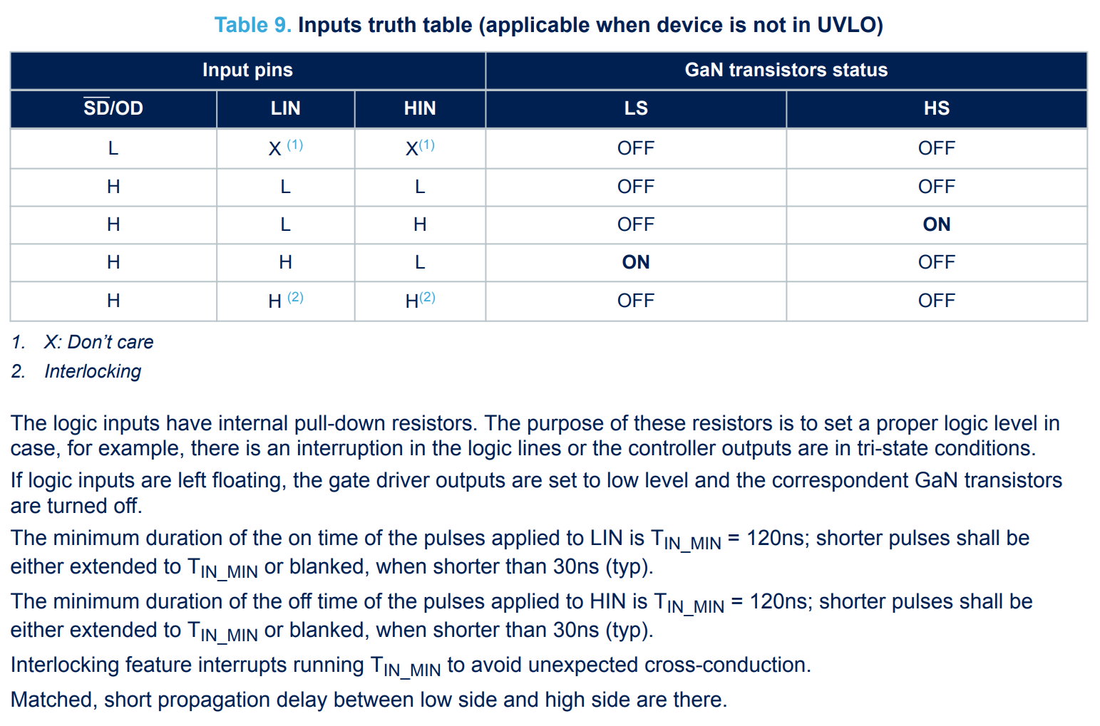
- The above DC bus waveform was shown with an 8kHz digital filter applied. Without any scope filtering there is a large amount of 40kHz switching noise riding on this 100 Hz signal. This could perhaps be improved with more DC bus capacitance. Electrolytics would be poor at suppressing such high frequencies so we’d need more MLCCs. I suppose this is why EMI filters are also present on the input to such converters.
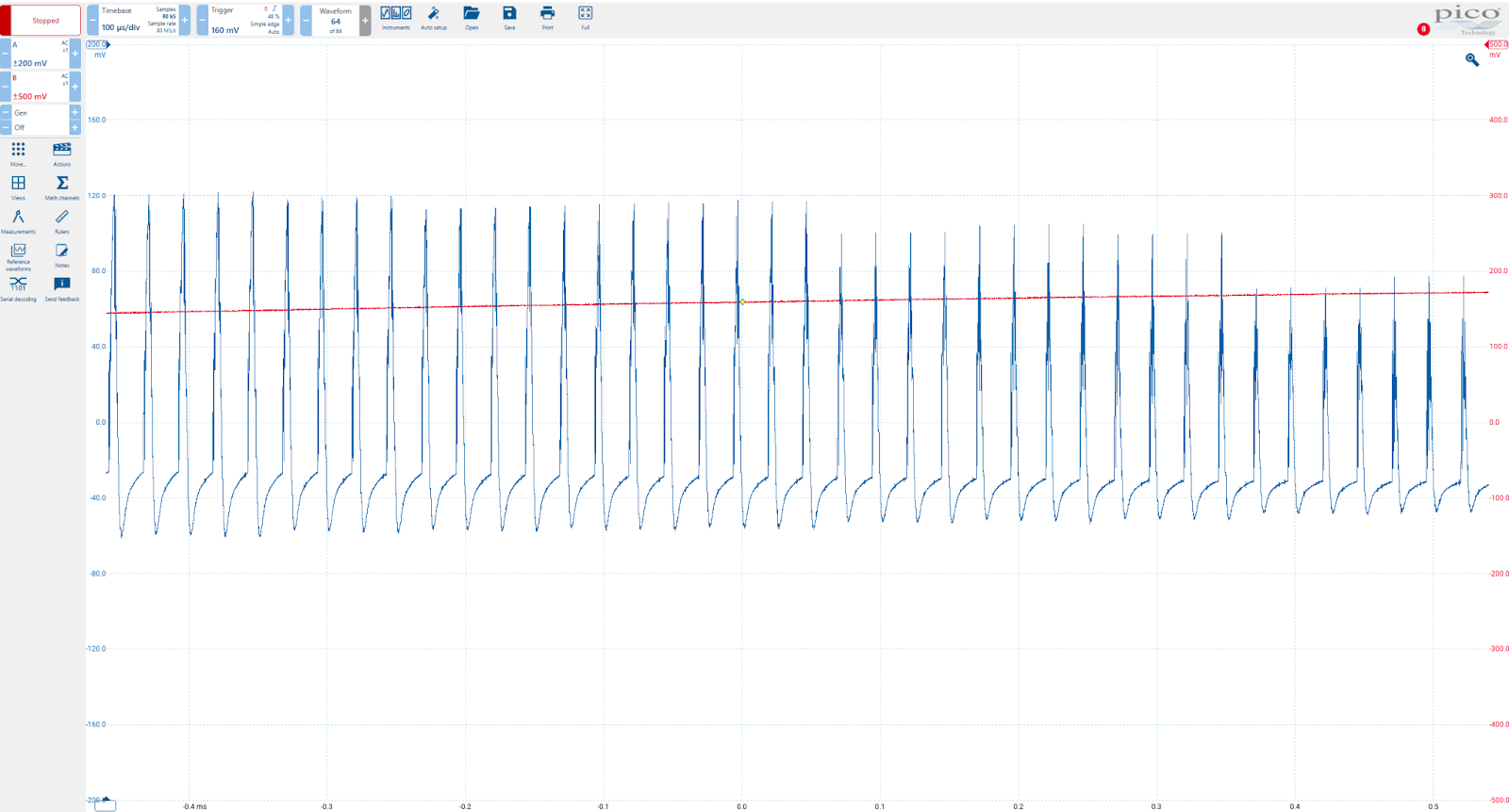
But let’s focus on our output waveform, it’s a stunner isn’t it!
Build an overload protection system
High speed cut-outs
Inverters can go up in a puff of smoke if an error occurs (incorrect - They explode with an ear splitting bang!). To protect against this we need to configure some interrupts. These will immediately disengage the MASTERGANs if the output current or DC bus voltage crosses chosen thresholds. If these errors are detected within ~1 millisecond it’s unlikely any permanent damage will be done to the hardware.
Conveniently the DFSDM peripheral has a built-in analogue watchdog feature. If configured thresholds are crossed it triggers an interrupt which could disable the output. But I couldn’t get this to work! So we’ll just have to set up another periodic function at 1kHz and check the vitals there. (Perhaps this was my downfall…)
Lower speed cut-outs
We guard against islanding by monitoring the grid frequency and grid RMS voltage. If these are out of range for more than 100ms we disengage.
- Grid RMS voltage > 255 or < 208???
- Frequency <49.5 or >50.5
Mains_RMS = Integrate_Mains_RMS(V_grid);
float Freq_Offset = PLL_PID.output * F_CONVERSION_K;

// These are high priority checks:
if(V_Bus > V_BUS_MAXIMUM)
{
	HB_Disable();
	Grid_Good_Bad_Cnt = GRID_UNACCEPTABLE;
	Error_Code |= 0b00001;
}

if(I_grid > I_OUTPUT_MAXIMUM || I_grid < -I_OUTPUT_MAXIMUM)
{
	HB_Disable();
	Grid_Good_Bad_Cnt = GRID_UNACCEPTABLE;
	Error_Code |= 0b00010;
}

// These are lower priority checks and have to be out of range for time
if(Mains_RMS > RMS_UPPER_LIMIT || Mains_RMS < RMS_LOWER_LIMIT)
{
	Grid_Good_Bad_Cnt -= GRID_BAD_FAIL_RATE;
	Error_Code |= 0b00100;
}

if(Freq_Offset > FREQ_DEVIATION_LIMIT || Freq_Offset < -FREQ_DEVIATION_LIMIT)
{
	Grid_Good_Bad_Cnt -= GRID_BAD_FAIL_RATE;
	Error_Code |= 0b01000;
}

if(V_Bus < V_BUS_MINIMUM)
{
	Grid_Good_Bad_Cnt -= GRID_BAD_FAIL_RATE;
	Error_Code |= 0b10000;
}

// Act on the above checks
if(Grid_Good_Bad_Cnt < GRID_OK && HB_Enabled == true) {
	HB_Disable();
	Grid_Good_Bad_Cnt = GRID_UNACCEPTABLE;
}

if(HB_Enabled == false) {
	if(Grid_Good_Bad_Cnt == GRID_ACCEPTABLE && ENABLE_JOINING_GRID == true) {
	    REQUEST_JOIN = true;
	    Error_Code = 0;
	}
}

// Constrain and decay any error counts
Grid_Good_Bad_Cnt++;
Grid_Good_Bad_Cnt = CONSTRAIN(Grid_Good_Bad_Cnt, GRID_UNACCEPTABLE, GRID_ACCEPTABLE);
Test thermal performance and efficiency at higher voltages
Now that everything has been working smoothly and we have a protection system in place lets crank up the DC bus voltage. We’ll connect a 140 ohm load to the output (A 400W flood light - in retrospect this was a stupid decision because the startup resistance is ~40 ohms until the filament gets hot). The plan was to watch things like a hawk as I cranked up the voltage. I tested 180V first then went up to 250V then 300V and finally 380V. It was uneventful.

Whilst outputting 250W into the flood lamp I measured 99.2% efficiency. The circuit was remaining less than 20 degrees above ambient according to some thermal imaging shots I took (unfortunately I did not take any IR photos of the actual mosfets - sorry). Very pleased with that efficiency. It was interesting to note that the MASTERGAN that was switching at 40KHz was the same temperature of the one that was switching at 100Hz. The switching losses in them are phenomenally low.


Build our PR controller
Time to implement the PR controller. I simply ported the code from the python simulations shown earlier. The controller runs at 13.3 KHz. I actually started with a PI controller and subsequently added in the resonant term too.
// -------------- Constants for the Resonant Controller:
float const kr = 5000.0;
float const Wdamp_50 = 2.0 * 3.1415927 * 0.75;
float const Wres_50  = 2.0 * 3.1415927 * 50.0;
float const kt = 2.6666666e4;	                 // kt = 2/Ts where Ts = 1/13.333KHz

float const a1 = 2 * kr * kt * Wdamp_50;
float const b0 = kt * kt + 2 * kt * Wdamp_50 + Wres_50  * Wres_50 ;
float const b1 = 2 * kt * kt - 2 * Wres_50  * Wres_50 ;
float const b2 = kt * kt + 2 * kt * Wdamp_50 + Wres_50  * Wres_50 ;

static float E_Prev2 = 0, E_Prev1 = 0, U_Prev2 = 0, U_Prev1 = 0;

// Calculations for the PI controller:
I_OUT_PID.setpoint = LO_Sample_256 * I_Output_Demand;
I_OUT_PID.input = I_grid;
PIDCompute(&I_OUT_PID);

// Calculations for the resonant controller:
float Ua = a1 * E_Prev1 - a1 * E_Prev2;
float Ub = b1 * U_Prev1 - b2 * U_Prev2;
float Ui = (Ua + Ub) / b0;

E_Prev2 = E_Prev1;
E_Prev1 = I_OUT_PID.error;
U_Prev2 = U_Prev1;
U_Prev1 = Ui;

float Demanded_Output_Voltage = I_OUT_PID.output + Ui;
Duty_Cycle = (int16_t)(Demanded_Output_Voltage * DUTY_MAX / V_bus);
The value I_Output_Demand determines the peak output current setpoint. The LO has an amplitude of 256 and so I_Output_Demand = 4e-3 then the setpoint peak current is about 1A.
Joining the Grid
Joining the grid is a critical moment. It involves engaging the MASTERGANs from previously being off, to switching. I thought the best moment to do this was at a zero crossing point (ZCP). When the grid checks are nominal a flag is set to REQUEST_JOIN_GRID. The controller then waits until the next ZCP before engaging the H-Bridge. We start with a low I_Output_Demand and ramp it up over a couple seconds.
I wanted a more real time method of seeing the output currents/voltages the inverter was measuring. I did this by using the STM32L475’s DAC and attaching a scope to its output. The metric to debug can then be written in real time to the DAC and the scope can see the values being measured. This works really well. The measured values had excellent resolution, were accurate and noise free.
Low Voltage Testing
Remarkably the PR controller worked on the first try. I adjusted the gains and it was performing brilliantly. It was interesting to note that at small bandwidths (eg. Wdamp_50 = 0.1) the resonant term would take time to grow in amplitude. Sorry for not having pictures of this! A bandwidth of 0.75Hz and Kr = 5000 worked very nicely.
The plot below shows the output waveform and the DAC outputting the LO’s phase_index which increments in 64-steps.

I was noticing small glitches in the output voltage waveform. Despite spending hours working out where these were coming from, I couldn’t find the source. Nevertheless the PI+R controller was nicely adjusting the output voltage waveform to drive a setpoint current. With a DC bus of 20V, I could short the output and the controller would immediately respond by reducing the output voltage to continue to drive the setpoint current. Excellent!
High Voltage Testing
I haven’t discussed how I am generating my DC bus voltages. I opened up a 12V 600W modified sine wave (MSW) inverter and connected wires to the DC Bus. When the inverter is powered with 14V it produces about 355V. I put a 25V LiPo battery in series with this voltage to get a 380V supply. The inverter was fed by a 30A SMPS power supply on my tabletop.
I figured I was still in safe waters driving the flood lamp and using DC bus voltages of 350V. I initially set quite a low I_Output_Demand. The current ramped up and lit the flood lamp dimly using the PI+R controller to meet the setpoint current. The setpoint wasn’t being reached so I had to set a higher setpoint than what I wanted delivered. With the lamp at half power of 200W the power supply was having to deliver about 15A to the MSW inverter
Eager to see the lamp flooding my shed with light, I increased I_Output_Demand. I saw my power supply current build through 4A, 8A, 14A, 20A and 24A before the circuit cut out. I was used to the grid checks cutting the inverter if something went funky. In the back of my head I felt a little uneasy. I’d heard a faint unfamiliar noise. I can’t remember exactly what occurred next. I believe I reset the circuit hoping the lamp would come on. A moment later a deafening bang and a blue spark the size of my fist erupted from a MASTERGAN. I froze and reflected on how dangerous the inverter had been all along. I switched everything off and took note of what had just happened.

Thoughts
- I think the MASTERGAN had undergone shoot-through. The DC bus would have discharged through the device and exploded it. Interestingly there was still voltage on the DC bus so perhaps the MASTERGAN had failed open circuit.
- Both upper and lower GaN MOSFETs in the package had exploded (2 little craters). I think this provides evidence it was secondary to shoot-through.
- Why had shoot through happened though? The MASTERGANs are supposed to have logic inside preventing shoot-through and we had programmed a dead-time.
- Perhaps an overcurrent situation occurred. I had a 2A fuse to the flood lamp but instead perhaps the grid side inductor saturated and a huge current flowed through the filter.
- If a single GaN MOSFET failed closed circuit it’d only take the other FET in the package to switch on to cause a shoot-through.
- Over-temperature - But the MASTERGANs have an inbuilt thermal cutout. They also never got hot in any of my earlier tests.
- It’s interesting that the explosion happened in the lower MASTERGAN. This is the package that only switches at 100Hz. Perhaps it hadn’t turned on properly. Or, perhaps it began to stop conducting properly within a switching period causing some sort of failure mode.
- Perhaps the 5V logic supply voltage to the MASTERGANs had gone out of range causing a failure. I think this is unlikely because the voltage regulators were working well within their specifications.
- Interestingly there are a number of failed capacitors. My best guess is that sparking jumped 380V within the chip. This would back feed all 5V bypass capacitors with 380V destroying them. It’d also damage all chips supplied with this rail.
- Could a resonance have built in the filter network causing a breakdown? I think this is an unlikely explanation.
- Could the PCB have broken down? I did have 380V between 2 copper planes spaced 0.11mm apart. However the dielectric breakdown of FR4 is supposed to be 20kV/mm. That’s ample in this case. Perhaps some moisture was in the wrong place. Nevertheless I wouldn’t expect this to cause the MASTERGAN to explode in this way.
- Perhaps the top MASTERGAN was operating at a high duty cycle (The limit used was 994/1000) Perhaps it’s high-side bootstrap capacitor discharge mid cycle. I can’t see how this would cause the bottom package to explode but it’s not out of the question.
Given the failure occurred at high currents, I think the most likely explanation is this: The grid-side inductor reached saturation causing an overcurrent situation. The bottom MASTERGAN low-side FET latched on due to the excess currents. The lower MASTERGAN then switched on its high-side FET and shoot-through blew the package apart.
Conclusion / Next
I will try again! I don’t want to give up until we have accomplished an open source 1kW hybrid inverter.
What has worked well:
- The AMC1306s and associated filters provide brilliant ADC measurements
- The PR controller looked extremely promising
- The MASTERGANs were operating with incredible efficiency. At 1kW the whole inverter may only dissipate 8W of heat.
- The isolation barrier works well and the components are well laid out.
Not so well:
- Having standard TO-220 MOSFETs might make the system more robust and fixable
- I must get the DFSDM analog watchdog working
- Is the filter optimal? Why are my inductors so big compared with powerful commercial inverters?
- Incorporate a UART interface for debugging/communications and breakout the DAC pin
I hope that this writeup has been educational or interesting. I have thoroughly enjoyed building version 4 and I have made good ground toward the final goal. Please leave comments and ask questions. I love hearing all your opinions and suggestions.