Grid Tie Inverter V3


I have built a 170W grid tie inverter. This is my 3rd iteration on the project. I’m nearly ready to get rid of the output transformer. I hope this writeup is either interesting or useful as a reference. The software and hardware files are on GitHub
Method Overview
Let’s quickly recap our general strategy. Grid tie inverters work by generating a waveform with the same phase and frequency of the grid but with a magnitude slightly higher so as to drive a forward current. This can all be done using 2 half-bridges and filtering.
Each half-bridge is working as a synchronous buck converter with its output voltage after filtering proportional to the PWM duty cycle. By varying the duty cycle in a sinusoidal fashion we get sinusoidal output voltages after filtering. We measure currents and voltages and with some software make ourselves a grid tie inverter.
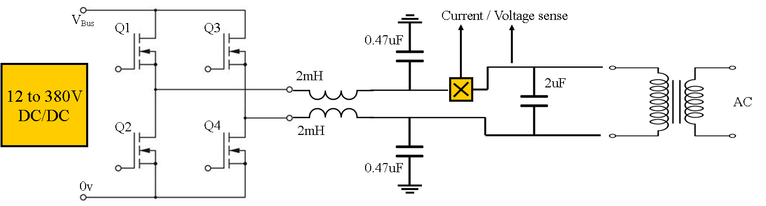
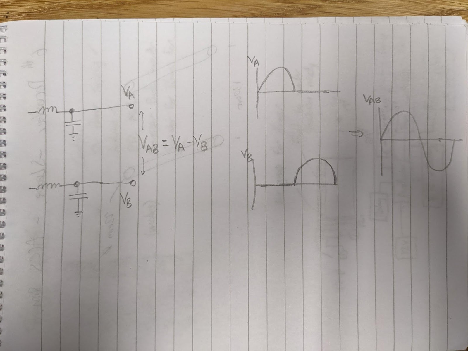
Each half-bridge can only generate positive voltages with respect to ground. If each half-bridge takes it in turns to sweep out half cycles then the differential signal will be a complete sine wave.
I use a cheap 12v to 380v DC/DC converter that I got off amazon for ~£15. These modules switch the input voltage at ~21kHz through a transformer. On the output of the transformer you get a square wave of the same frequency but with a voltage magnified by the turns ratio. Depending on the taps used you get 160,220 or 380V. These voltages do depend on the input voltage, with a 10V input you get 186V on the 220V tap and at 15V you get 280V.


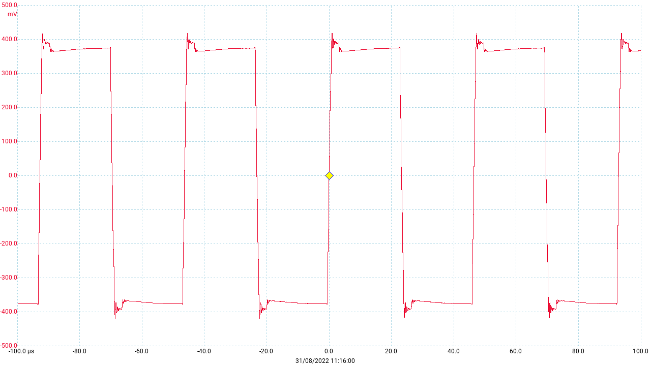
Waveform on the 220V tap with the input voltage at 10V and using a 500x probe (21kHz)
The outputs from this unit need a full bridge rectifier to convert them into DC voltages. That’s simple enough, I built my own with 600V ultrafast diodes. These modules also provide an isolated 18V winding which after regulating down to 12V and 3.3V is useful for our gate drive and logic power on our main inverter board.

Overall these parts produce our high voltage DC bus and separate 12V gate drive supply
I designed and assembled a 4-layer PCB which houses an H-Bridge, the MOSFET drivers, hall-effect current sensing, some voltage dividers and an LC output filter. I’ll discuss all this in more detail later.
The inverter board which is the heart of this project
I’ll explain the software in later but the general parts include a phase locked loop (PLL) to synchronise to the grid. I sample the output current and use a 64-FFT to measure the phase and magnitude of the 50Hz fundamental along with the 150 Hz, 250 Hz, 350 Hz harmonics. PI controllers are used to inject inverse harmonics for each frequency to cancel them out. This allows us to achieve low distortion levels in the output current. The phase and magnitude of the fundamental is continuously adjusted to drive the desired output current and minimise any reactive components.

Layout of circuit with the black/red output wire heading straight to the transformer
I hope to get rid of the transformer very soon. I’m just a bit nervous to generate 240V signals directly and feed them straight into the grid. I feel like the transformer offers a bit of a buffer and it provides isolation. The transformer dissipates 10W of power doing nothing. So it’s a big, heavy, efficiency loss and must go soon!
Flaws From Previous Versions
There are so many flaws to address in the previous versions (GTI1, GTI2) it’s hard to know where to start. Here is a list of the problems I identified.
- Improve EMI by better use of ground planes on the PCB
- Improve EMI by having the LC output filters close to the switching transistors
- Improve EMI by having our LC output filter capacitors referenced to ground on each phase
- Improve EMI by better choice of DC bus capacitors and their locations
- Use toroidal inductors
- Improve software by implementing harmonic compensation
In order to avoid the need for an output transformer we must eventually raise the DC Bus voltage to about 380V so we can directly synthesise a 240V AC waveform. Electromagnetic Interference (EMI) became a big issue as I increased the bus voltages on version 2. It completely corrupted the current sensing for me and I was noticing huge spikes of interference on my oscilloscope. I suppose this can be expected if you switch 380v signals with nanosecond edge rates. PCB layout design becomes as important as the schematic itself.
Better use of ground planes
The switching nodes are the traces connecting each pair of transistors. The layout and design of these are key for EMI containment. Initially I thought it best not to have a ground plane underneath this node since surely any capacitance to ground would present an energy loss during each voltage transition? However it turns out a 1cm² PCB trace directly above a ground plane on a 1.6mm 2-layer board only presents a capacitance of 3pF. Charging 3pF to 400V at 40kHz uses 10mW of power. The power loss is insignificant. Instead, placing a ground plane underneath the switching node significantly reduces EMI..
I designed a 4 layer PCB with power and ground as inner layers. I asked this question on stackexchange to help decide between a split analogue/digital ground plane or one continuous ground. The general advice was to have a single ground plane.
Position the LC output filter close to the switching node
Previously, I had flying wires coming from the switching node going to a separate filter circuit board. This was an awful design in retrospect! In this version the switching nodes feed straight into onboard LC filters with traces kept as short as possible and above the ground plane. This minimises emitted EMI I believe.
LC output filter capacitors referenced to ground
I was never quite sure about the output filter design. I’m still not certain I have optimised this. Commercial inverters all seem to employ LCL filters but I haven’t got my head around those yet. There are several possible configurations which are discussed here on StackExchange. Bobflux suggests these output filter layouts and outlines their respective merits and pitfalls.

Variety of output filters suggested on StackExchange by Bobflux
In my previous GTI versions I was using layout 2. I’ve changed to layout 4 in this GTI iteration. The key difference being that each LC output filter is referenced to ground. This allows the 41kHz ripple current to travel through the grounded capacitor and return straight into the DC bus capacitance. It reduces the area of the current loop which reduces EMI. I think this is a particularly important improvement.
My filter design is illustrated below and has a resonant frequency of 1.6kHz. This is relatively close to the logarithmic mean of the 50Hz desired signal and the 41kHz undesired PWM switching frequency. The 0.47uF capacitors are ceramic MLCCs, the 2uF bridging the output is a polypropylene type. Both these capacitor types offer low parasitics, namely low resistance and inductance..

Output filter and values used in this GTI iteration
For reference the reactance at 41kHz of
0.47 uF is 8 ohms, 2.0 uF is 2 ohms, 2.1 mH is 541 ohms
At 50Hz:
0.47 uF is 6.7 kohm, 2.0 uF is 1.6 kohm, 2.1 mH is 0.66 ohms

Frequency response of the filter - using LTspice
Thinking about ripple current
Why choose these component values? The first decision is the inductance. There’s a general rule of thumb for switching power supplies like this. The rule is to have the peak-peak ripple current to be 20-30% of the maximum output current. Assuming a peak output current of 2A we should therefore aim for a ripple current between 0.4-0.6A.
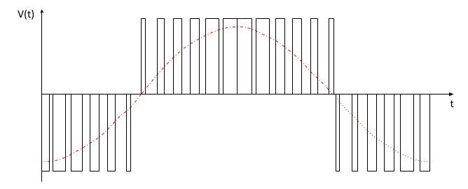
PWM duty cycle varying at different parts of the sine wave
The ripple current depends on the duty cycle. The ripple is largest at 50% duty cycle. However at the peaks of the AC waveform the duty cycle won’t be 50%. A 240Vrms sine wave peaks at 340V which would require a duty D = Vout/Vin = 340/380 = 90% (assuming a 380V DC bus).
We have a switching frequency of 41kHz. With a DC bus voltage of 380V our ripple current through a 2mH inductor when outputting 340V will be 0.44A. There’s an excellent article by TI describing all these calculations and here’s an online ripple current calculator. It follows that at our peak output current of 2A we have a 22% ripple. I did these calculations backwards to find an appropriate inductance and settled on 2mH.
It’s important to factor in the ripple current when choosing your inductor. The ripple current superimposes on the peak output current. The inductor must not saturate. With a 2A peak output and 0.44A ripple the maximum current our inductor must handle is 2.22A.
I played around on LTspice simulating different capacitor values and seeing the impact on resonant frequency. The values chosen give a resonant frequency through the load of 1.6kHz. The 0.47uF capacitors are MLCC rated to 630V with a X7R dielectric. These are quite stable as far as temperature is concerned but they’re not tremendous at maintaining their capacitance with a DC bias voltage. The peak of our signal swings to 340V which is 340/630 = 54% of their rated value. The following graph from the wikipedia article on ceramic capacitors suggests >25% capacitance loss at this voltage (perhaps 35%). We should therefore expect the 0.47uF caps to behave as 0.31uF caps at the peaks of the sine wave voltage swings. This will affect the filtering of the PWM carrier but I don’t think it’ll be the end of the world.

Variation in X7R dielectric MLCC capacitance with bias voltage - Bad!
A nice 2uF polypropylene capacitor does the rest of the filtering (these aren’t bothered by temperature or bias voltage, but are a lot bigger).
Use Toroidal Inductors
I have switched to using toroid inductors. Toroids do a better job of containing the magnetic flux inside them and not radiating it. In hindsight all GTI teardowns I've seen employ toroids. You have to wind your own and this requires consideration of 1) Intended inductance, 2) Saturation current.
I chose this magnetic core material which has a permeability of 90. This particular core had an AL = 128nH/Turn^2. This means 1 turn around it produces 128nH, 2 turns generates 2^2 x 128 = 512nH, 100 turns generates 100^2 x 128 = 1.28mH. I (tediously) wound my own 2mH inductors for the output filters with ~125 turns of 21AWG (0.71mm diameter) enamelled wire. They ended up being 2.1mH with a DC resistance of ~65mR.
Estimating saturation current
Cores have their limits. Beyond a certain applied magnetic field strength (H = NI/L) the B-field in the core material will stop changing ie. the core becomes saturated. This is very bad because it means our all important inductance starts to reduce.
Micrometals provides a calculator for use with a variety of core materials. With the core I have used (FS-185090-2) with 125 turns we get some interesting data.

Inductance of the toroidal inductors made for this GTI as a function of DC current
This useful graph shows us that we can have currents up to 2.5A before the inductance drops below 90% and 3.5A before it drops below 80%. We should therefore just manage to output 250W (2.3Arms (3.2A peak) into a 110v load). If we were outputting into a 240V load we could probably manage 500W.
The calculator also provides us with core losses. All inductor cores suffer losses due to hysteresis. For a 2A 50Hz RMS output with a 41KHz 30% ripple the calculator estimates a 6.9W core loss. That’s ok, it’ll only be experienced by the core which is undergoing switching, which is alternated every half cycle. On average, each core will experience half this power loss, 3.5W is manageable.
What does the core material of an inductor do? It allows you to perform a trade off between saturation current and turn count. With an air core you’d have no saturation current limit but you’d need a prohibitively large number of turns to achieve 2mH. On the other end of the spectrum some ferrites have permeabilities over 5000. A core with such a high permeability may only need a few turns to achieve 2mH but it will saturate at uselessly low currents (a few milliamps!). You won’t be able to store any energy in such an inductor because energy stored E=½ L I^2.
Air gaps are introduced (either discrete gaps or in powered cores they are distributed) to dilute the permeability to a desired value. For a required inductance, you want to choose a relative permeability which allows a sensible trade off between number of turns (e.g. 125 turns) and saturation current( e.g. 2.5A). If you want a higher Isat you can either choose a lower permeability and increase your turns or you can physically increase the volume of the inductor core. In the end it all comes down to compromises. Increasing turn counts usually necessitates thinner wires and this obviously worsens parasitic resistance.
Poor DC bus capacitance
When the H-Bridge transistors switch they immediately suck or push current into the DC bus. The DC bus needs capacitance to absorb these transients because the power supply is located many centimetres away and will have inductance enroute.
Not all capacitors are born equal. A large fat electrolytic may have good capacitance but it will have large parasitic inductance and resistance. MLCC ceramic caps can respond and absorb the currents much faster leading to lower voltage spikes and less EMI from the DC bus. I have positioned 0.1uF MLCCs right by the MOSFETs, a 10uF PP film capacitor mounted on the PCB and the bulk capacitance is provided by a 470uF 400V offboard electrolytic.
Design Process
Schematic
The general layout is similar to before. I have done away with isolation and rather opted for parts that are simple and available. When I eventually remove my output transformer I will populate the optoisolators allowing for UART to be sent/received for debugging/control.
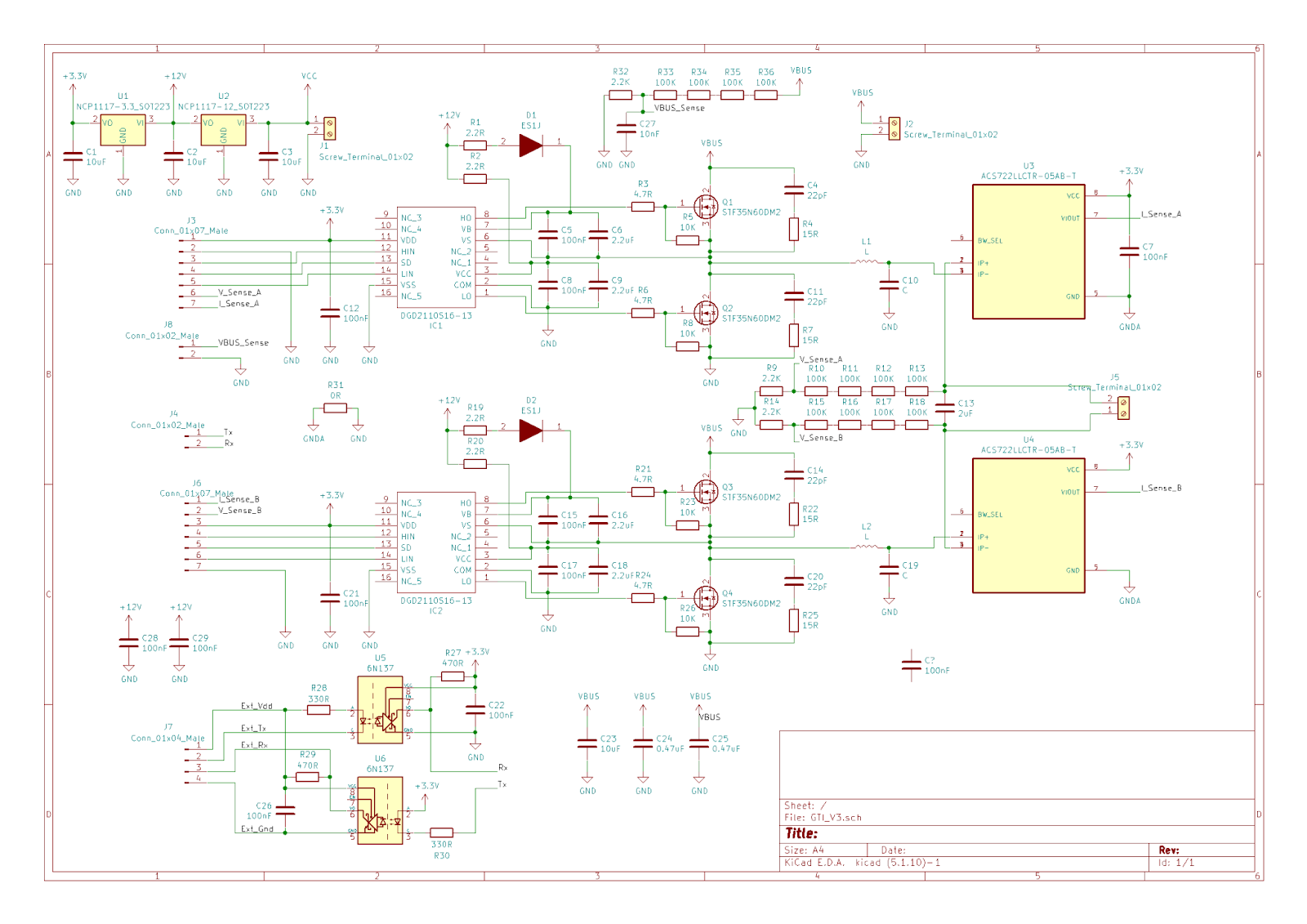
GTI Schematic
The parts used include:
- DGD21105 - a straightforward high speed high voltage MOSFET driver
- ACS722 - a decent hall effect current sensor with various ranges, I went for 5A version
- STF35N60DM2 - MOSFETS, good ones!
There’s not much to say about the schematic as it’s all pretty standard. The voltage dividers use 4 series resistors to limit the voltage across each part. Resistors have voltage limits. Why have I used 2 current sensors? Well it allows us to measure the common and differential mode output currents. This is important because we don’t want to output any common mode current. It also doubles our measuring resolution.
PCB Design
It’s a 4-Layer PCB. Every effort was made to minimise the loop area of the gate drive and return paths. I’m happy with the result. I allowed for the addition of snubber caps and resistors but haven’t populated these.

GTI PCB 4-Layer board showing continuous ground plane and split power planes.
Of note, I routed 3.3V power and ground from the quieter left side of the PCB to the ACS722 current sensors on the right. I thought this would be better than using a via to the local ground plane since there are large ground currents flowing in the vicinity that may cause the local ground plane voltage to vary with respect to the ground voltage on the quieter side. I don’t know if this was a beneficial choice.
I could have shifted over the inductors and large central 10uF capacitor 5mm leftwards closer to the MOSFETS. I did make a tiny error (corrected in the schematic and PCB layout shown here) which meant I had to add some little wires to the pins on the DGD21105 drivers. (I forgot to connect a pin on each package to ground!)
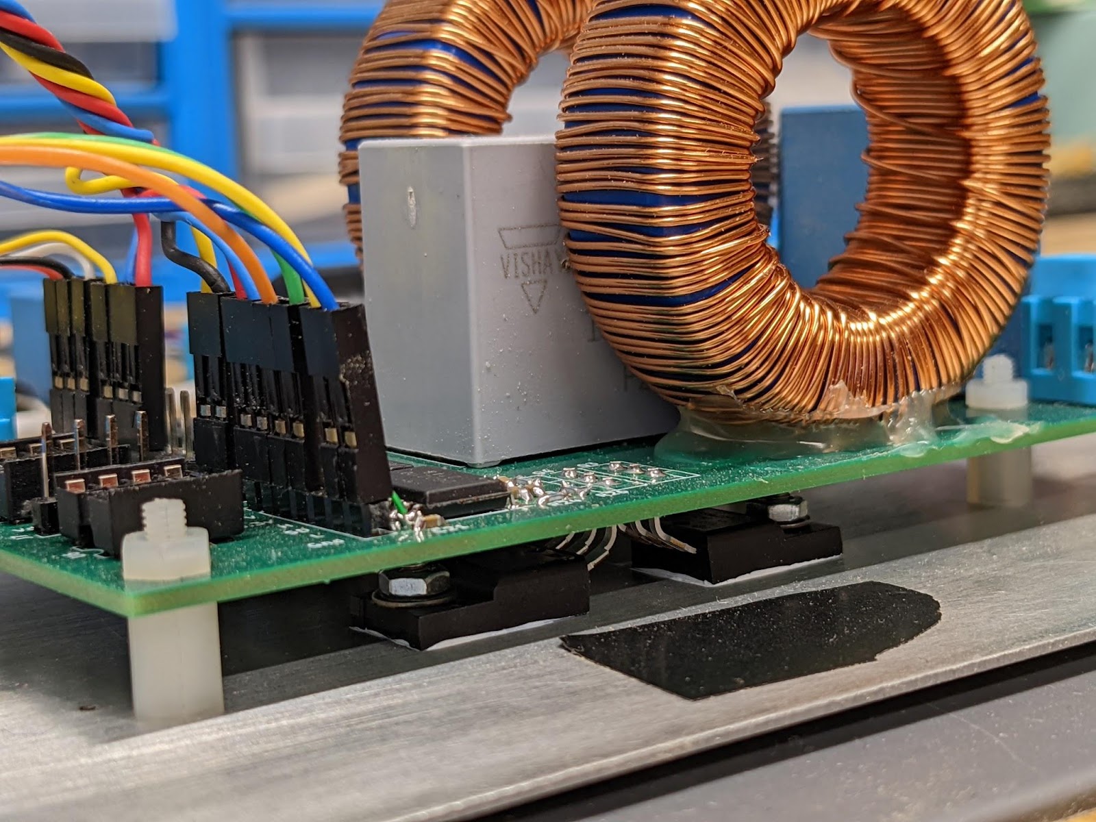
The MOSFETs are bolted to an aluminium plate to keep them cool
The MOSFETS bolt down onto some aluminium which works as an excellent heat sink. Their packages are made of plastic so they don’t need any insulation.
I made a row of headers to connect to an offboard STM32F4 development board. Having those wires is ugly but it makes testing easy. In future I could build a dedicated card that pushes onto these headers and houses the STM32F and its oscillator. It’s crazy though, STM32F4’s are just completely out of stock for the foreseeable future!
Software
The software is the cornerstone of this project. It’s what I’ve been scratching my head about most. Let's discuss the general operating principles:
- We measure the DC Bus voltage, the output voltage and the output current using the STM peripherals
- We implement a PLL which synchronises a local oscillator (LO) to the 50Hz grid voltage
- To join the grid we wait for a zero-crossing point before engaging our H-Bridge
- We output a sine wave in phase and of the same magnitude as the grid.
- We sample each period of the measured current waveform. Stored as 64 samples per 20ms period.
- We perform an FFT on this sampled current waveform to get the various frequency and phase contents
- We run a PI controller for each sine and cosine harmonic at (50,150,250,350Hz). By injecting inverse harmonics into our output voltage we clean up out output.
- We run checks on our bus voltage, grid RMS voltage and frequency, output current. If anything goes AWOL we disengage our H-Bridge to protect our hardware.
Measuring Voltages and Currents
The STM32F407 houses 3 independent ADC modules. ADC3 is configured to be triggered by timer2 at 1kHz and it continuously reads our DC bus voltage. The DMA continuously overwrites a variable in main memory with fresh values.
We configure ADC1 and ADC2 to run in dual regular simultaneous mode such that they sample at exactly the same time. This is important because the hardware provides us with 2 single ended voltage readings from each half-bridge leg. Only by taking the difference can we find the overall output voltage. Similarly, we combine the current sensor readings to get the differential output current.
ADC1 is triggered by timer3 at 20KHz and ADC1 triggers ADC2. They are configured in scan conversion mode so on the 1st trigger ADC1 samples the voltage of phase A and ADC2 samples the voltage of phase B. On the next trigger both ADCs move to the next channel and therefore ADC1 samples the current on phase A and ADC2 samples the current on phase B. This process then repeats.
The DMA is configured to transfer the data from ADC1 (which gets ADC2’s samples too) to main memory. The data is packed into a 32bit word for each sample such that ADC1’s reading is stored in bits 15..0 and ADC2’s is in 31..16. The DMA is configured so that it fills a circular 2 word buffer. The 1st word being the voltage readings and the 2nd being the current readings. Each time ADC1 completes a scan it calls an interrupt and we run the following call-back function.
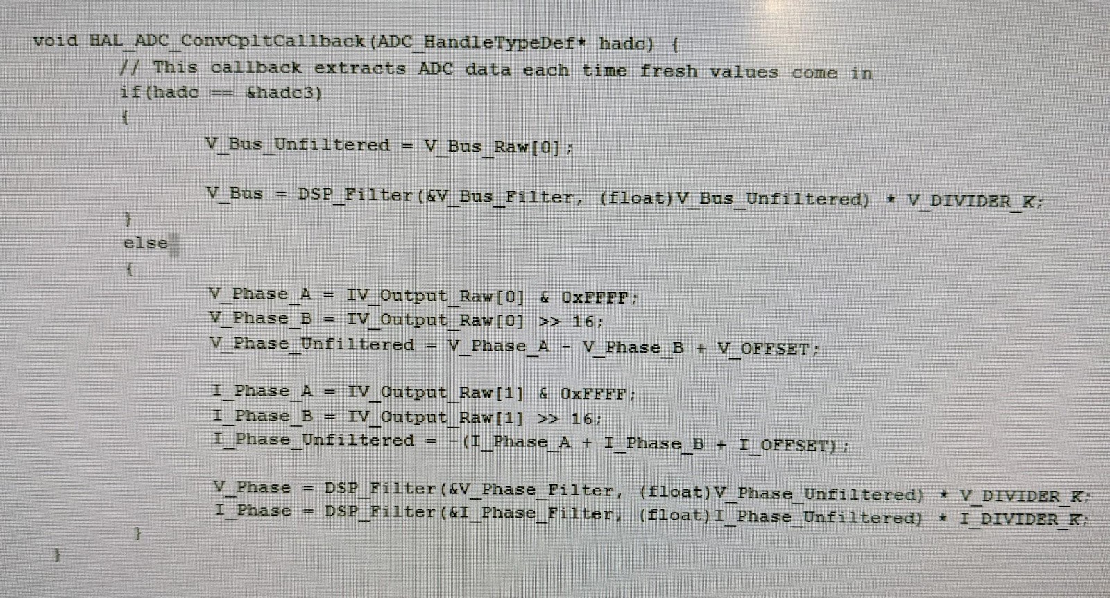
This function unpacks and puts the data through a low pass 1st order filter. V_Phase and I_Phase are then available for the rest of the program for use and are automatically updated.
Phase Locked Loop
The code for the PLL is remarkably simple but the maths behind it is a little more involved. We run a local oscillator (LO) which naturally oscillates at 50Hz. This is done by having a 256-sample lookup table of cosine values. An index increments through this at 256x50 times per second. We can marginally slow down or speed up this incrementation rate to vary our LO frequency.
Each time we increment our LO index we calculate the multiple of our LO and grid voltage samples. We then keep an integral of these multiplications over exactly the last period (normalised to the grid’s RMS). Both the LO and the grid will have pretty much the same frequency 50 +/- 0.2 Hz. The integral should be zero.
If the phase difference between the grid and our LO is not exactly 90 degrees (ie LO = cos and grid = sin) then the integral will be non zero. For small phase errors the integral result is proportional to the phase error. This is very useful because we can use this error signal to speed up or slow down our LO signal to bring this phase error to zero. We do this with a PI controller shown in the 3rd line which can make small adjustments to the base increment rate of out LO.
Not only do we have a 50Hz LO but also LOs running at the harmonic frequencies of 150, 250, 350Hz. These will be used later.
Every 4th increment we store the output current sample such that we maintain a 64-sample buffer of each 20ms period. Once the period is complete we will calculate an FFT on this data to analyse the frequency content.
FFT Based harmonic correction
Unfortunately the grid voltage contains harmonic distortion. If we simply output a 50Hz sinusoidal voltage these harmonics will induce harmonics in our output current. We don’t want our output current to have distortion so something must be done.
We can address this by:
- Sampling our output current waveform - we take 64 samples per period
- After each 20ms period we perform a 64-FFT on the samples
- This gives us the frequency content of all the harmonics in the signal. To expand on this, the FFT of 64 real samples (Input[64]), returns 32 complex numbers (Output[64]) representing:
- Output[0] = DC component
- Output[1] = 0
- Output[2] = 50 Hz Sine magnitude
- Output[3] = 50 Hz Cosine magnitude
- Output[4] = 100 Hz Sine magnitude
- Output[5] = 100 Hz Cosine magnitude
- Output[4] = 150 Hz Sine magnitude
- Output[5] = 150 Hz Cosine magnitude etc
- We want to eradicate all but the 50 Hz sine component.
- To do this we inject inverse sine/cosine harmonics into our voltage signal for each frequency that we don’t want.
- We use a PI controller for each harmonic component and adjust our injection amount so as to bring the measured current component to zero. For example, if we measure 60 mA of 150 Hz cosine harmonic we’ll add in some inverse 150 Hz cosine harmonic to our voltage output.
- Every period we re-measure the amount of output distortion and keep adjusting all our respective injection harmonics until only the 50 Hz sine wave is left.
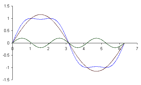
Harmonic distortion - Blue signal is from the addition of the other 2 traces
I decided only to bother with correcting the 150, 250, 350 Hz harmonics because they make up most of the THD. The method works really nicely but the transient response is slow. The PI controllers run after each 20ms FFT calculation and make small incremental adjustments. Hence it can take hundreds of milliseconds to finally adjust the output waveform to be distortion free.
Joining the Grid
A GTI has to join the grid at some point. It must switch on its MOSFETs and start outputting a voltage. This is a critical moment because if we generate a different voltage than that present on the output a large current will flow.
To join the grid I do this a few seconds after booting up after all grid checks are complete and when our PLL is locked on to the grid signal. I wait for a rising zero crossing point before enabling the MOSFET drivers etc. We start by blindly outputting a 50 Hz sine wave in phase with the grid and of equal magnitude. Over the next few seconds the FFT based harmonic correction will clean up our dirty output.
Grid Checks and anti-islanding
As with previous version of this GTI we measure and check these parameters are in range else we disconnect:
- Bus voltage
- Output current
- Output RMS
- Output frequency
Testing


Well as you can see in the video it works. I can do 203 Watts continuously. I measured 1.68Arms@121Vrms output for a 22A@11.4VDC input which equates to 203W / 252W = 80% efficiency. Not great, but not too bad. I don't really know where all the losses are because nothing gets particularly warm except for the cheap DC-DC step up converter. I had to position a fan blowing air over its MOSFETs
I still have lots of improvements to make with the software. I just wanted to get this all published to draw a line in the sand. I think I may add back in some PI current control with the FFT correction system helping out too. My output waveform isn't too bad. I'm going to get rid of the transformer and make these changes without it.
There have been some substantial improvements in this version, but I must admit that Grid Tie Inverters are complicated and working on this project whilst doing my full time job is tricky. That's why there's been about a years gap between each version!
As always - I'd love to read any comments you have.
Future Improvements
- Get rid of transformer
- Improve efficiency
- Higher powers - aim 250-500 Watts