GERBER FILES
Abstract:
People talk different languages, while programs and files do too. Due to the busy world we’re living in today, designers have to be quicker in communication. This was the key of having many files, each file has its own language leading the worker to get it done either by bare hands or machines. In this article we will get used to understand what the Gerber files mean, why should we use it and how to create them.
Introduction:
Electronics field has many jobs required to be done before running the circuit actually. Some of these are very basic like drawing the schematic, some are intermediate like simulating visually to maintain the errors or mistakes, and some of them are considered to be the last touches like making the PCB. PCBs are usually made by the fabrication manufacturers, which means that they need to know what to do by having the guidelines according to the PCB. Here comes the role of the Gerber files, as they simplify the customer’s needs to be followed by the manufacturer as it’s the way of connection between both. Gerber file is the standard format for the design data transfer of PCBs, it’s like the backbone of the electronics fabrication industry. All PCB design systems can export Gerber files and all PCB fabrication software can work upon them, enabling PCB specialists to exchange PCB design data in both secure and efficient ways. It holds the standard ASCII vector format to describe copper layers, legend, solder mask, drill data, and all essential details to obtain the board picture.
How to Export the Gerber Files of PCBs


Firstly, we need to know which software is used to generate this format. Different soft wares can generate this format like EAGLE, EASYEDA, or KICAD for example. By using the KICAD, we will do simple and easy steps to export the Gerber files.
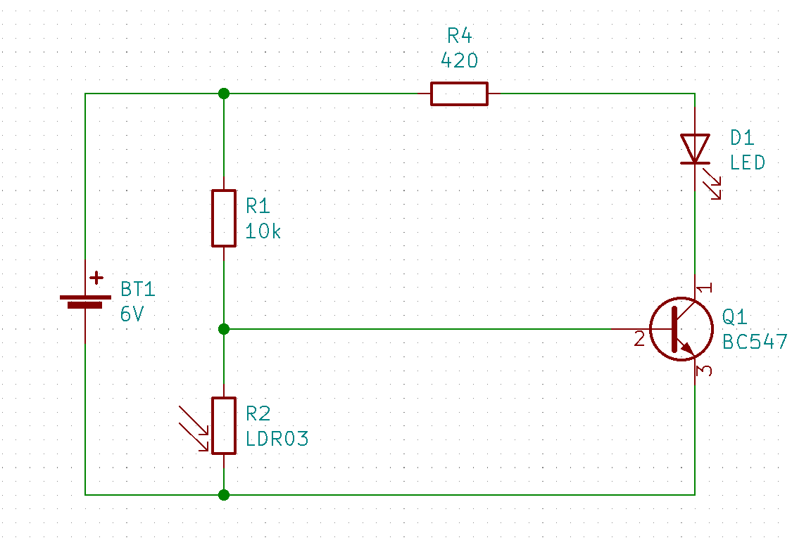
1- First, we need to have a fully defined schematic as shown in figure (1).
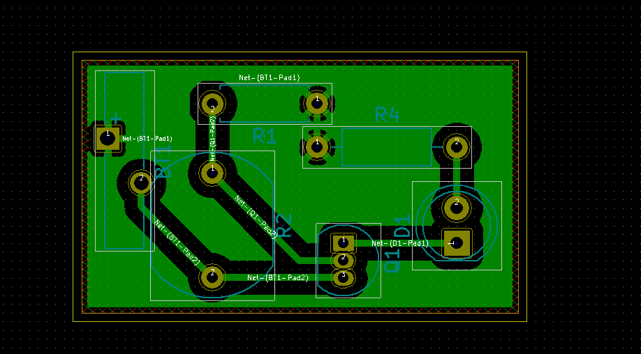
2- Opening the PCB editor in figure (2).
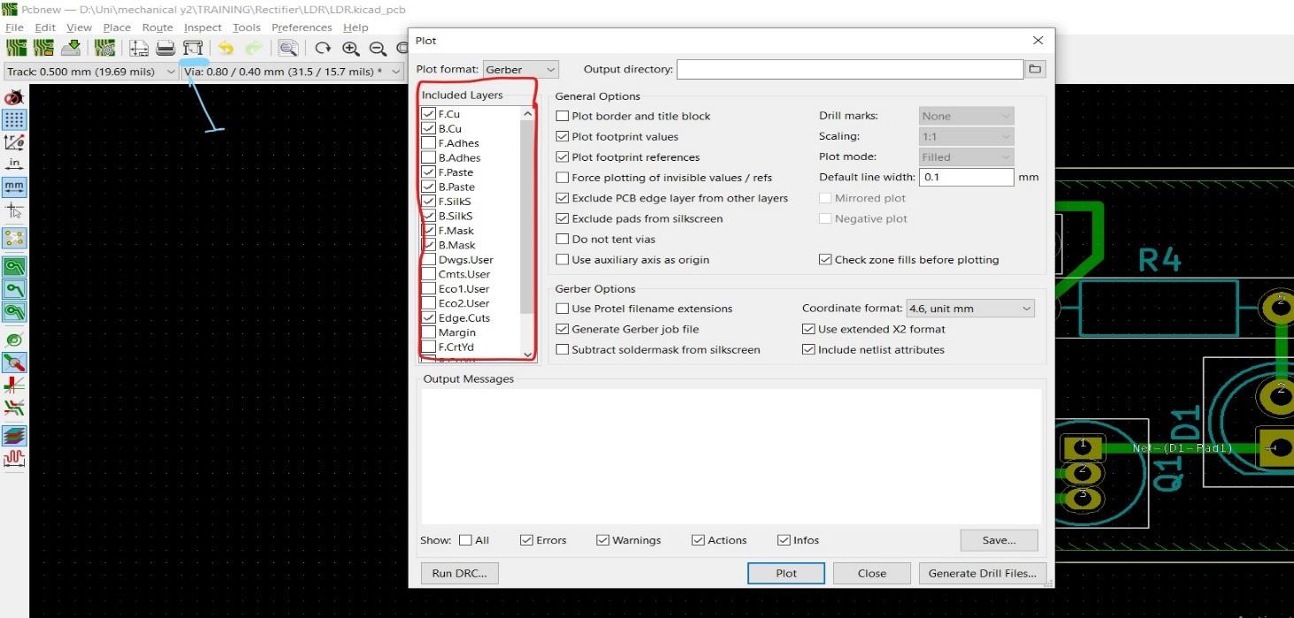
3- Select “Plot”, then a window will appear as in figure (3).
You can see in this widow the options you need to take care of when generating the files. The list within the red boundaries is the layers list, where you can check which layers you want to include in your files. The other “General Options” are the plotting options, like plotting the values or references, etc.
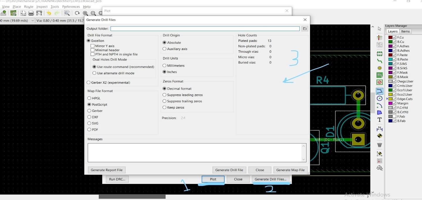
4- Select “Plot” from below actions, then “Generate Drill files”. After that, another window will appear as shown in figure (4).
5- Here where you can generate and save your Gerber files on your PC.
6- After saving, you can check and view the files you exported by going to the project and select “Gerber Viewer” as shown in figure (5).
7- Select “Open Gerber files”, then select all the files you need to view as shown in figure (6).
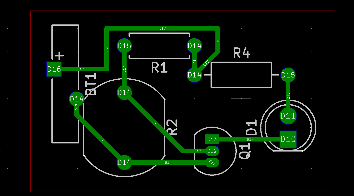
8- For example, I chose some layers to view in figure (7), and here’s my Gerber view.
Conclusion
Drawings, outlines, datasheets, and any leading instruction format nowadays are very import as the communication language between engineers, designers, and workers. Thus, this language has to be studied carefully to make it easier for those people to communicate, innovate, and produce, even if they are living miles apart. These are the science languages.