How to Design Circuits and Create a PCB Using Autodesk EAGLE
by Mipy in Circuits > Electronics
3135 Views, 16 Favorites, 0 Comments
How to Design Circuits and Create a PCB Using Autodesk EAGLE
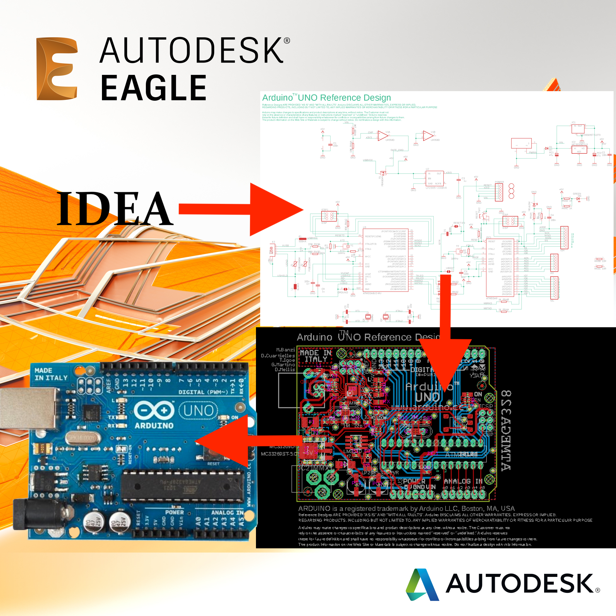
There are many kinds of CAD (Computer Aided Design) software out there that can help you design and make PCBs (Printed Circuit Boards), the only issue is that most of them don't really explain how to use them and what they can do.
I have used many types of CAD in the past and I have to admit that EAGLE is by far the best, most powerful and easiest to use. I am not just saying this because it is owned by Autodesk, and so is Instructables. I truly believe it is the best option out there for both beginners and professionals. (Plus, if you're a student you can get it free for three years!)
In this Instructable, I am going to teach you, step-by-step, how to install EAGLE, how to design a circuit, and use the parts list, and then convert it to a PCB.
Installing EAGLE

The first step in creating your PCB is... surprise surprise, downloading the software to do so. EAGLE is supported on most operating systems and can easily be obtained from Autodesk's website.
1. First, go to https://www.autodesk.com/products/eagle/overview and click on the "subscribe" button in the middle of the page; it will then ask you to select what plan you want.
2. Now it will prompt you to either sign in or create an account.
3. You will have the option on how to pay, select which operating system you want and the version. The product will then download. To install, follow the instructions on the installer wizard.
Getting Started
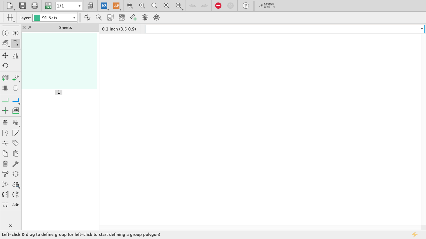
The moment has arrived, you now can open it for the first time! Once you have opened it and signed in, you will be greeted with the control panel. This is where you can find your designs and models, and see new update info.
To create a new schematic:
1. Click on "File" at the top of the page, then go to "New" > "Schematic." This will bring up a new window in which you can start making our schematic.
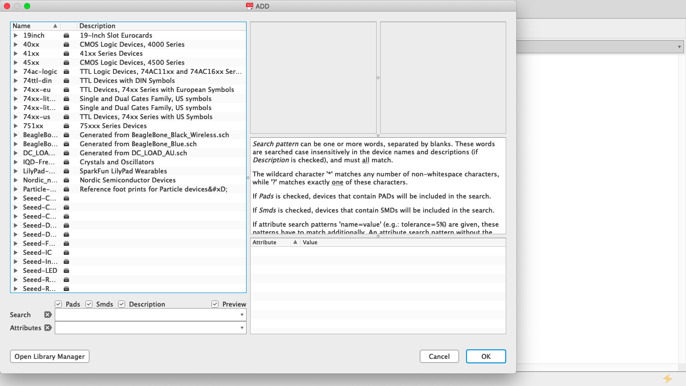
2. Begin by installing the libraries for the parts you want to use. To do this click on "Add Part" on the sidebar. This will bring up yet another window in which you can select parts to add and use. You will need to download the parts libraries.
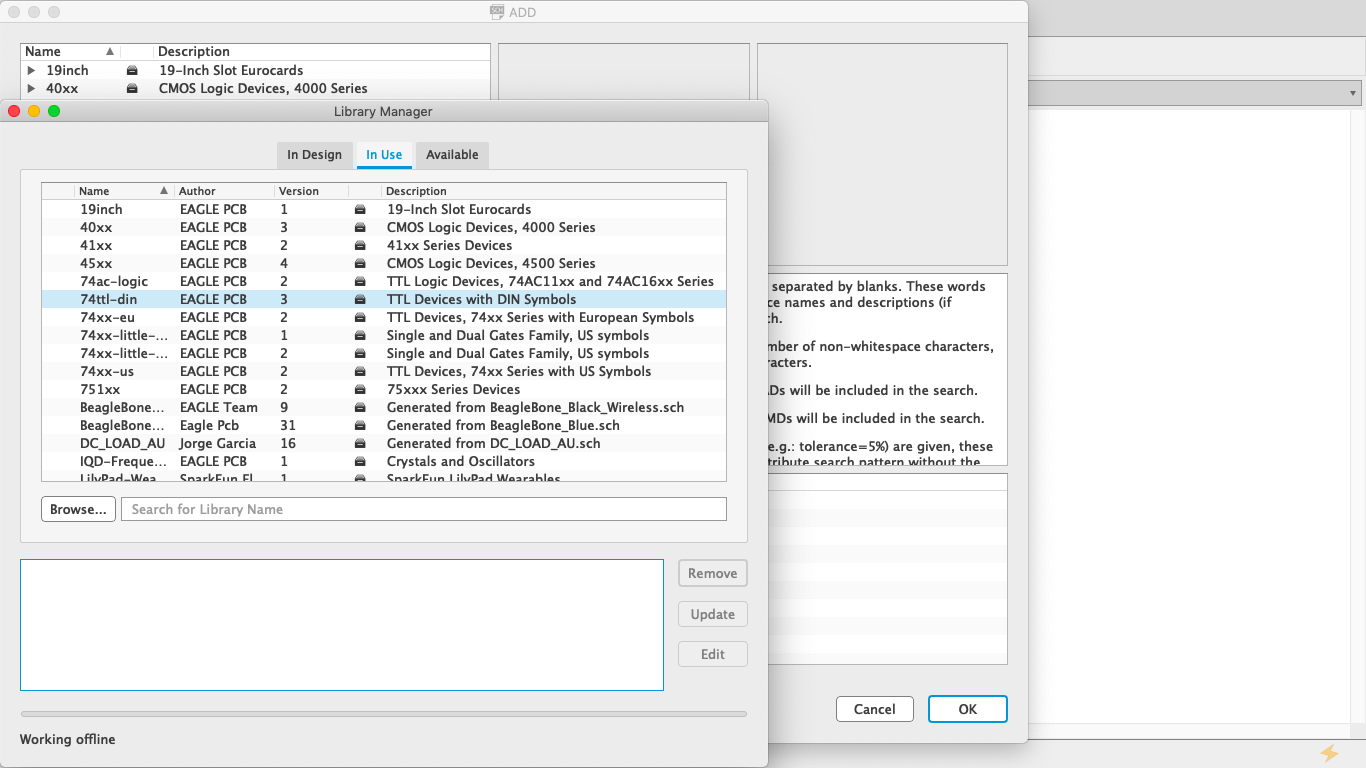
3. To do this, click on "Open Library Manager" in the bottom left corner. You will see another window; click on "Available" on the middle-right. This will show you all the possible part libraries that EAGLE has to offer. You can choose whichever ones you want to download but I recommend using them all.
4. After you have highlighted the ones you want, click on "Use" in the bottom right corner of the window. This will start downloading all the parts libraries you selected. This may take a while so now would be a good time to get a snack and get ready to start making your schematic and board. Once all the Libraries are downloaded, you can close the "Library Manager" window.
Creating Your Schematic
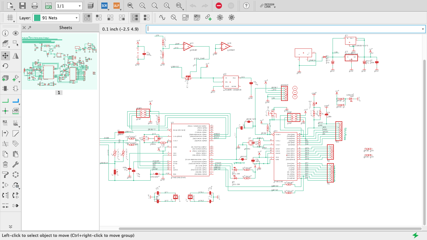
1. Begin your schematic by searching for the parts you want in the "Add Part" window is already open (or select it in the sidebar). Once you have found the part, double click on it and it will bring you back to your schematic.
2. To place the part, click on where you want it to go. After you have all your parts laid out, select "Net" in the sidebar to draw the connections between the parts so you know where to draw the traces (the copper wires inside the PCB).
3. To do draw the traces, have "Net" selected and hover your mouse over the pin of the part you want to connect. When a green circle appears, click on it and then click on the pin you want to connect it to.
To delete a part, select "Delete" in the sidebar and click on the centre of the part you want to delete.
To move a part, select "Move" in the sidebar and click on the centre of the part you want to move, this will make it turn bright red. Move it where you want and click again to place.
To rotate a part, select "Rotate" in the sidebar and click on the centre of the part to rotate it 90º clockwise.
To create GND(Ground) or VCC(Voltage at the Common Collector) connections, go to the "Add" menu and search for VCC or GND.
You can also add annotations, shapes and text by clicking on those features in the sidebar.
There are so many other ways to manipulate your parts and design that I won't even go into them in this basics tutorial. Check them out under "edit" at the top of your screen. I recommend playing around with them even if you don't know what they do.
Have fun creating your schematic and have a play around with the different tools EAGLE has to offer.
Laying Out the Components for Your PCB
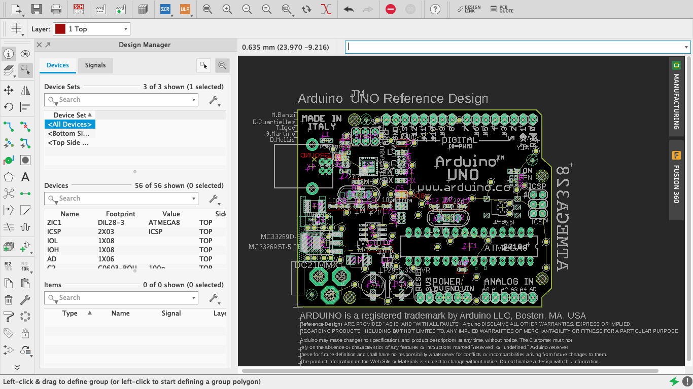
The time has come to create your board!
1. Once you have successfully created your schematic, save it and then hit the "Generate/switch to board" button on the top left of the interface or under "File" at the top of the page. This will bring up a new window with a black background and all of your parts lined up in it.
2. If you would like to change the shape of the board that you are laying your parts out on from the default, click on "Layer" in the top left corner of the interface and change it to "Dimension." This means that you are now editing the dimensions of the board itself.
To change them either click on one of the corners of the pre-existing rectangle and drag it to whatever size you want, or go to "Draw" at the top of the page and select which type of shape board you want (rectangle, polygon, circle, etc).
3. Now you have created a suitable board, it is time to start laying out your components. Click on whichever component you would like to place and drag it to the desired spot on the board. To change which side of the board a component is on, click on the "Mirror" option on the sidebar and select the component(s) you would like to swap sides.
To rotate a component use the "Rotate" function on the sidebar.
4. Once all of your parts have been placed it is time to start creating traces. These are copper wires that will create electrical connections between your components. To add these, you have two options: Either use EAGLE's auto-router feature to automatically create traces (if you do this skip to step 7), or draw them manually.
Creating Your Own Traces
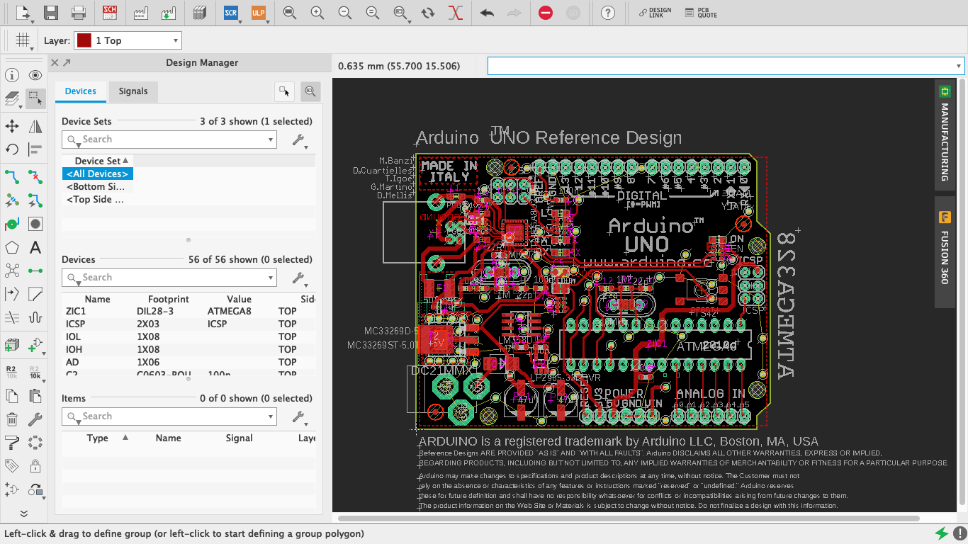
1. To create your traces manually, first calculate what thickness you want them to be by using a trace width calculator. I use https://www.4pcb.com/trace-width-calculator.html (not sponsored), however you can use any one you like.
2. Once you have determined what thickness trace you want, click on the "Layer" dropdown and select which layer you want to create first. Select the "Route" function on the side bar. To make the trace your desired thickness, use the "Width" setting on the top-left of edge of the interface.
3. Create the trace by selecting whichever pin/leg/pad you want as the start of your trace. The trace should appear as a red line extending from the start of the trace to your mouse. In addition, you should also see yellow lines extending from the end of the trace to a pin/leg/pad; these are the electrical connections you designed in your schematic.
4. To make a connection, click on whatever pin you would like to attach your trace to. If you want to make your trace go around something or have a corner, click on where you want the trace to turn and then move your mouse to wherever you want the next corner or connection to be. Keep doing this with all of your connections until there are no yellow lines left. Try not to create 90º angles because these are hard to manufacture; instead use two 45º angles to connect traces.
5. If you want to connect between layers, use the "Via" function on the sidebar. This creates a connection between the top and the bottom layers in the form of a small dot.
6. If you want to create holes for mounting, use the "Hole" function on the sidebar. To change the size of the hole, right click on it and select "Properties" and change the "Drill' settings accordingly.
Creating a Groundplane & Silkscreen
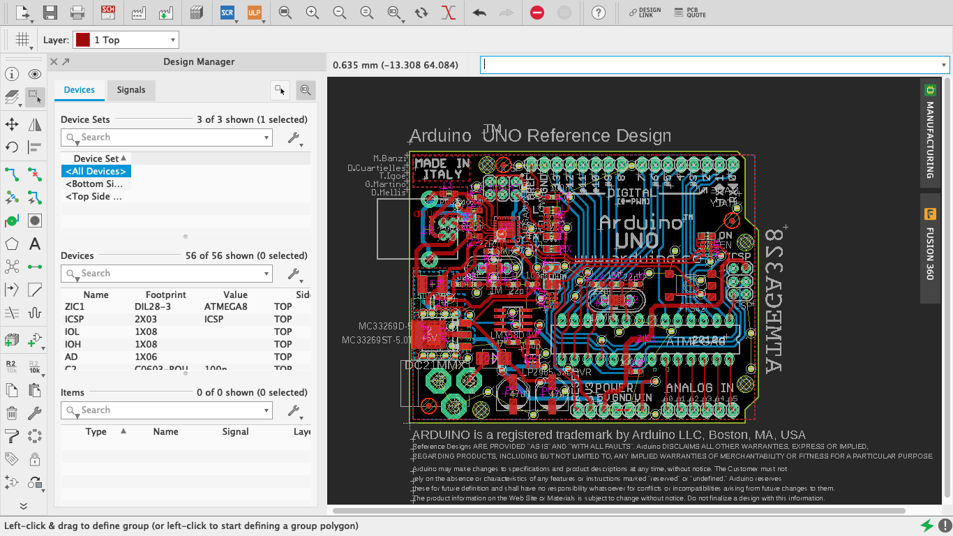
There are many different styles/layouts of PCBs, for beginners. I recommend one of two: either connect all of your components together directly with traces. Alternatively, create all of your connections except the ones connecting to ground and then have the rest of the layer entirely, or mostly, a solid copper ground-plane (this creates all of the ground connections without having multiple traces). In the diagram above, the blue lines are the traces on one layer and the red is the solid copper layer (the ground-plane). The blue traces are connecting all of the non-ground connections and the red layer connects all of the ground connections.
1. Select which layer you would like to work on using the "Layer" setting in the top left corner. Once you have selected the layer, use the "Polygon" function on the sidebar and draw the outline for whatever shape ground-plane you want.
2. Make this the ground-plane, after you have made all the other traces you want, by clicking on "Ratsnest" on the sidebar. The rest of the board will then become the solid copper region. To change the clearance between the ground-plane and the traces from the default, adjust the "Spacing" setting in the top-right of the interface.
3. To finish your board off, you can add a silkscreen. This is a thin layer of ink printed onto the surface of the PCB to show the orientations, positions and components (these are done for you automatically unless disabled/removed.). It can also be used for decorative purposes.
4. If you want to add text or shapes to the silkscreen, change the layer you are editing using the "Layer" setting in the top left corner to "tPlace" or "bPlace." This will change the silkscreen on the top or the bottom layers respectively. Use one of the "Draw" functions in the sidebar to create whatever pattern/design you want.
If you have followed the last two steps, feel free to skip Step 7.
Using the Autorouter
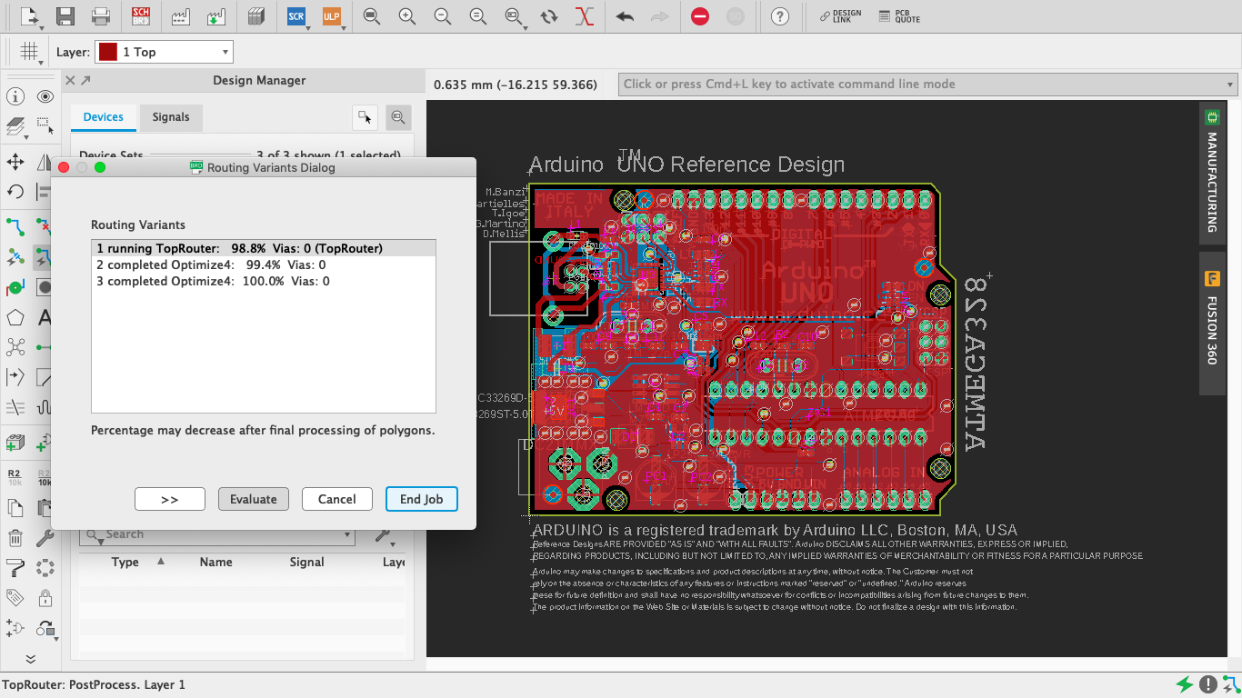
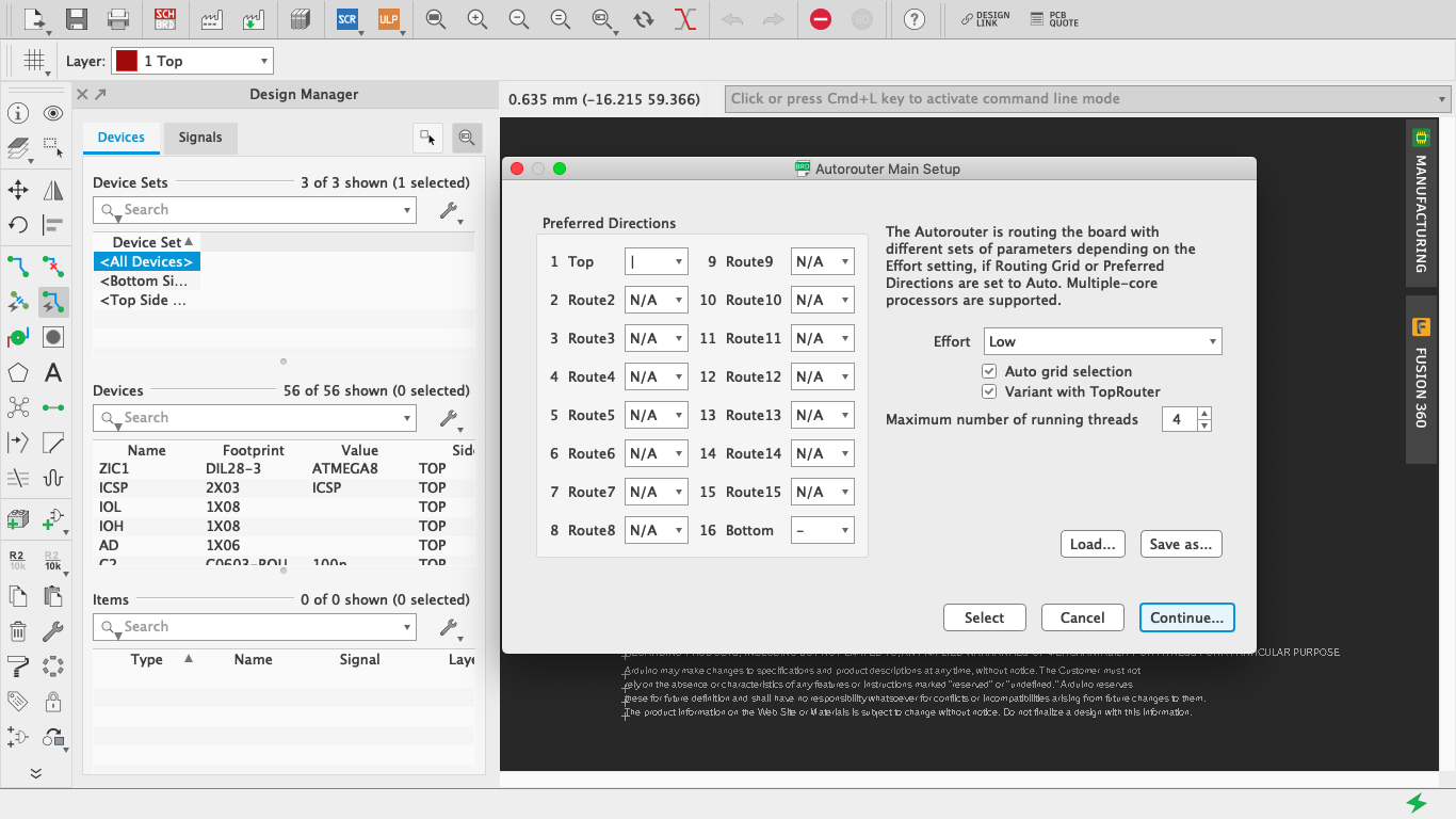
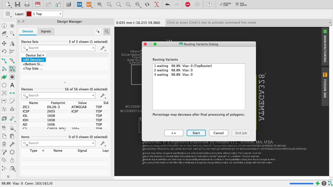
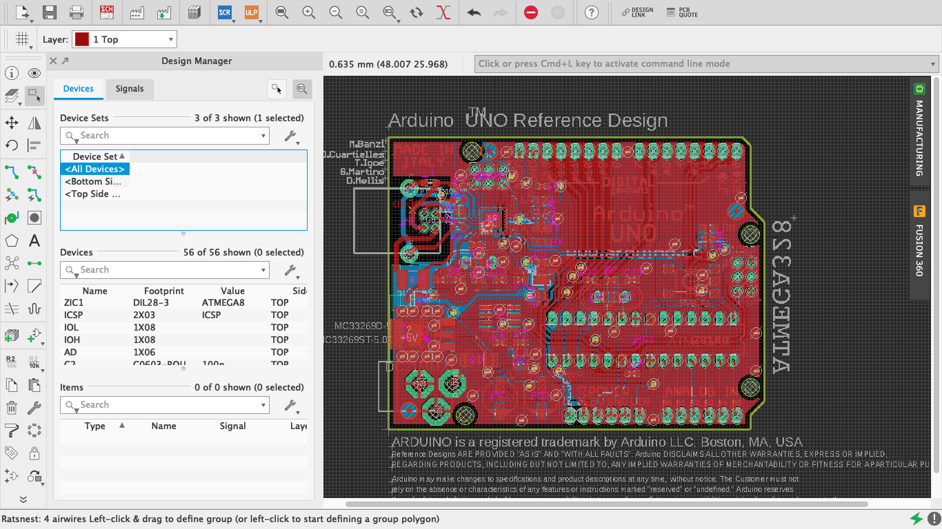
Instead of manually drawing all the traces, you can use the autorouter. This function uses an algorithm to draw the traces for you. This is very useful if you don't have a lot of time or can't be bothered to do it manually. However, it will take some playing around with the settings to get it to work well. And, as good as EAGLE's autorouter is, it still isn't perfect and you will still need to look over and adjust its work.
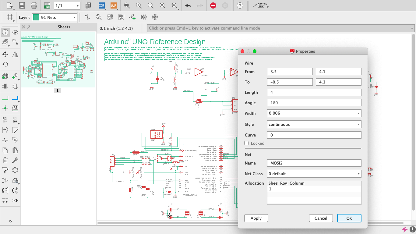
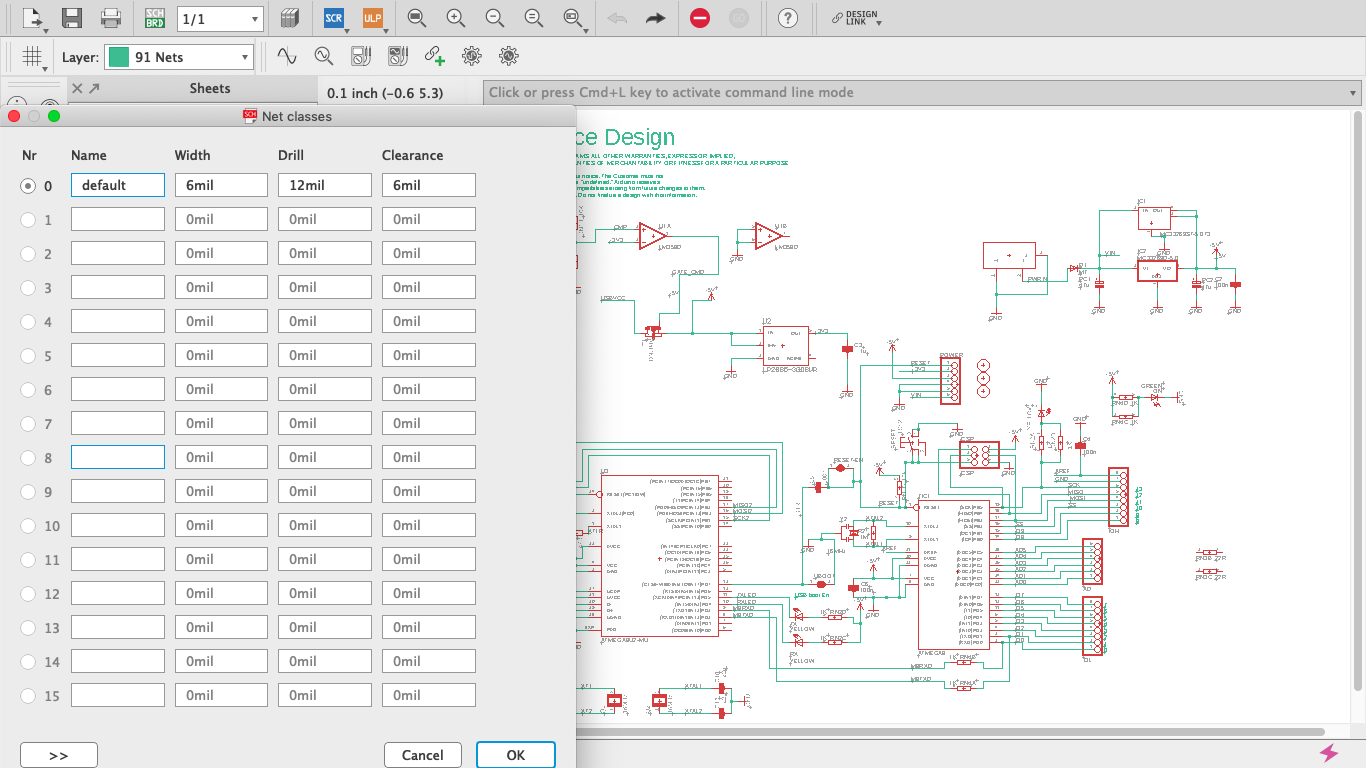
1. To use the autorouter, you will first have to let the software know what width you want different traces to be. To do this, go back to Schematic View and select "Edit" > "Net Classes." This will bring up a new window with lots of different rows in it.
In the first one, change the "Width" setting to the desired width of a standard trace; this is the default and will automatically set all of the traces to this width (you can change them later).
2. If you would like some traces to be wider, go to the row below the first and rename it (eg: Ground). Then you can change the width and other settings however you want. Repeat these steps for every different-sized trace you want on your board. Once you are happy with your changes, hit the "OK" on the bottom left.
3. To change different traces to different size settings, select the "Info" function on the sidebar and click on the trace you would like to change. Now click on the "Net Class" dropdown menu near the bottom and select which option you would like. Hit "OK" when you are satisfied.
4. You are now ready to run the autorouter: go back to PCB View and hit the "autorouter" function on the sidebar. A new window will appear with all the settings for the autorouter showing. For a basics tutorial, none of these are important so just hit the "Continue" button at the bottom and then click "Start." The software will then do its thing. This may take a while so sit back and relax for a bit.
Once it has stopped making changes, click "End Job" and look over the PCB to fix any mistakes it might have made.
Exporting Gerbers and BOM for Fabrication
You are finally done designing your PCB! Give yourself a pat on the back for all the work you put in. You deserve it.
Although you have just finished making our schematic and board design, the fun has only just begun. This step shows you how to take your idea and design and turn it into reality (ie: creating a physical PCB).
1. If you want to order your PCB design from a professional service, you can either use the "PCB Quote" function on the top-right of the interface. This will take you to Element14's PCB fabrication service. Follow the instructions on their website.
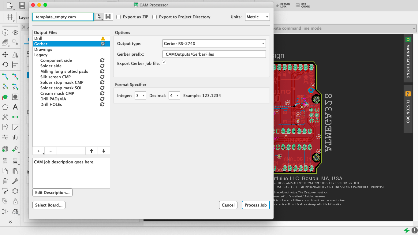
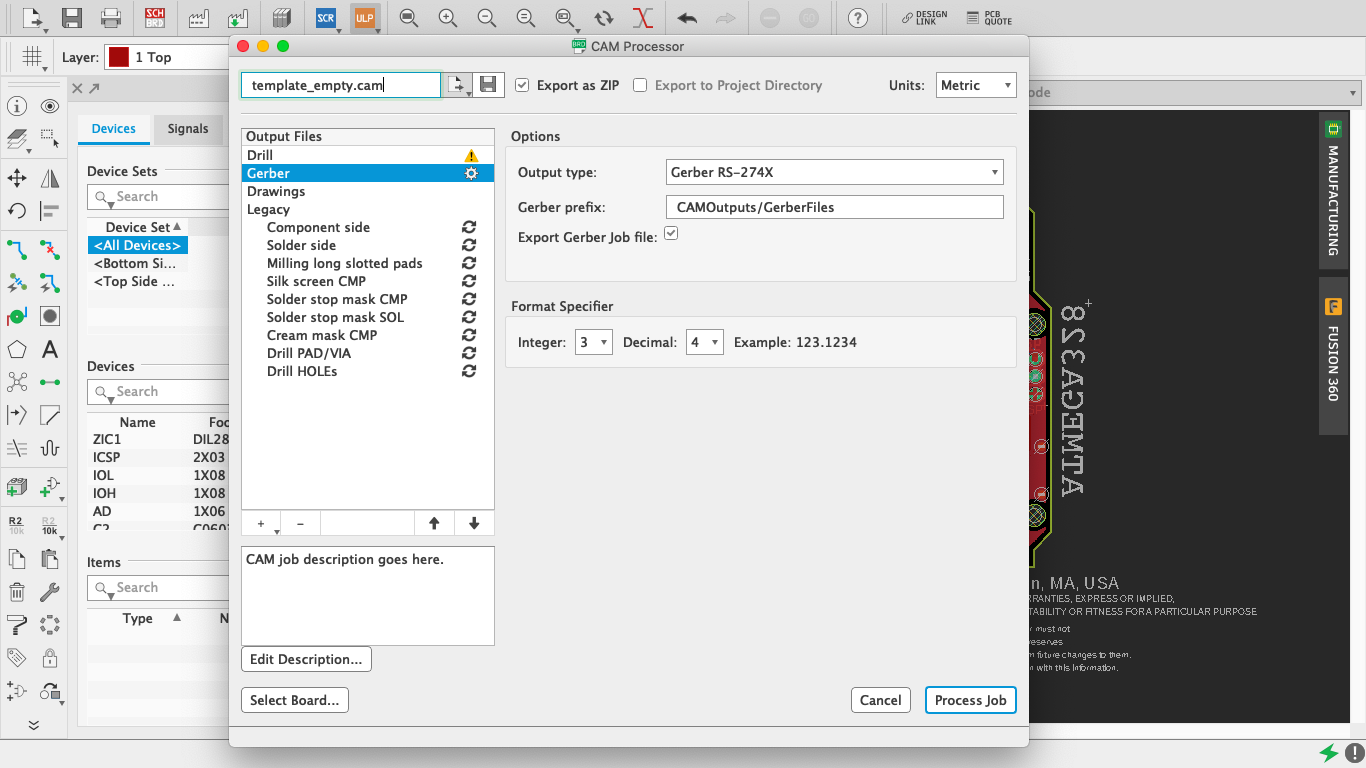
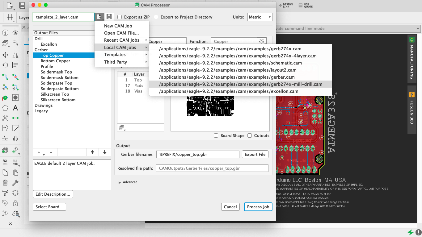
2. If you would like to get it fabricated by some other manufacturer, you will have to export the Gerber files (files containing the information of your PCB design). Do this by using the "CAM Processor" function on the top-left of the interface.
A new window will appear: click on "Load Job File" > "Local CAM Jobs" > "gerb274x-mill-drill.cam" on the top left corner of the window. Check the box next to the dropdown labelled "Export as ZIP."
Click on each layer on the sidebar one at a time and make sure that "Mirror" under "Style" is NOT selected, ie: deselect it.
3. Once you are done, you can hit "Process Job" in the bottom left corner of the window. Another window will open where you can save your work wherever you want.
You can now send it to whatever fabrication service you like, order the parts, and get soldering!
4. Alternatively, you can etch the PCB yourself. To do this, I recommend Yeo Kheng Meng's article on how to export an image to do this: "http://yeokhengmeng.com/2016/03/eagle-file-to-diy-pcb-etching/" (not sponsored).
5. To create a B.O.M. (Bill Of Materials) to order the parts, go to Schematic View and use the "Run ULP" function on the top left of the interface. This will bring up a new window, select "BOM" and hit Enter. Adjust the settings to your preferences and then save your work.
Conclusion
Congratulations, you have made it to the end of the Instructable! You deserve a medal. I know it was long but it is just so hard to fit so much content into a single instructable.
I hope that now you have the knowledge and skills to install EAGLE, design a schematic and turn it into a PCB. Although this Instuctable may have seemed long and complex, it actually isn't that hard if you break it down into simple steps.
If you have any advice, suggestions or questions, please leave them in the comments section. These are invaluable to me because it will help me to improve my later Instructables.
If you think I deserved your vote in the PCB Contest, please do so below.
I wish you the best of luck making and, as always, have fun!