FPGA Composer
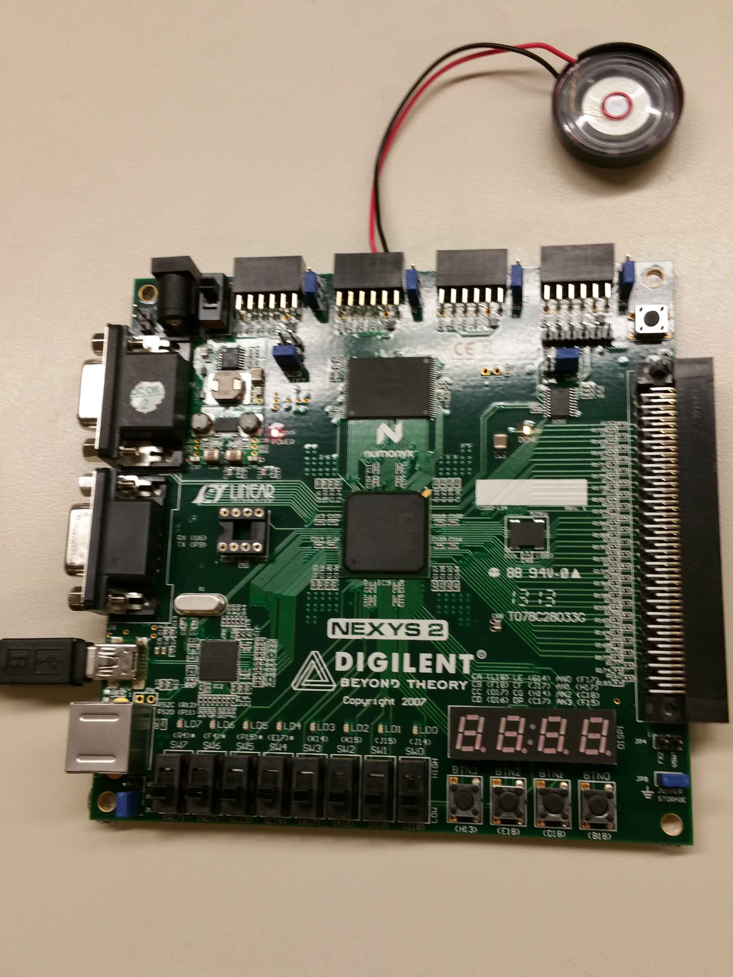
This instructable will guide you through the design and construction of an electric keyboard/ composer. A composer functions like a piano. When a key is pressed, a corresponding note is played. Since these are fun to mess around with, they make for a fun project. The composer will be made up of a nexys board connected to a speaker. This connection will allow for the board to output a signal that the speaker can then play. Keys for the keyboard will be routed through the switches on the board. Switching on a switch will play the corresponding note based on its precedence. Precedence is simply which note is played if two or more switches are on. Precedence is that A plays over B, B plays over C and so on. This means that if A is switched, it will always play because it is first.
This project will make use of Xilinx for writing the VHDL. Xilinx is a software tool that enables the user to create and synthesize VHDL. Following the synthesis, the VHDL can then be used to program the nexys board. The board is then connected to the speakers for a completed composer.
What You Will Need
Nexys Board FPGA
Xilinx ISE
Speakers of some kind
Auxiliary cable to connect board to the speakers, or some other wiring setup
Gathering Project Items
Gather all of the required items for the project (i.e. the board, Xilinx, the speakers, and the aux cable). Begin by purchasing a nexys board if you have not done so already. These can be purchased directly through Digilent or through a external seller like Amazon. Following this, visit www.xilinx.com to download Xilinx. Lastly, get the specified speaker system and auxiliary cable. Then, become familiar with VHDL and proficient in using Xilinx. This will ensure that no confusion will result from the following steps.
Creating the Project in Xilinx
Open Xilinx and click new project. When the screen opens,
give the project a name, specify where you want to save it and set top-level source type to HDL. Then click next. Then specify all of the details for your given board. This varies based upon which version of the nexys board you possess. We used a nexys 2 because it is the cheapest. The details for the nexys-2 board are as follows:
Evaluation Development Board: None Specifice
Product Category: All (or General Purpose)
Family: Spartan 3E
Device: Nexys-2: XC3S500E
Speed: -4
Top-Level Source Type: HDL
Synthesis Tool: XST (VHDL/Verilog)
Simulator: Isim (VHDL/Verilog)
Preferred Language: VHDL
Then click next. The following page will give a screen to specify the inputs and outputs. This will set up the first part to simplify the work. Begin by giving a name to the signal and it’s corresponding in or out. The signals are as follows:
a: in
b: in
c: in
d: in
e: in
f: in
g: in
clk: in
audioout: out
Then click next. On the next screen ensure that all of the details are correct then click finish. This will open up the new project.
VHDL Background
This step will give you a little bit of insight as to what all of the different parts of VHDL actually do. For the creation of the composer, we will need to specify the entity, architecture of the project and two separate process blocks. The entity is the basis for the inputs and outputs, the architecture will specify each of the signals and there values, and the process blocks will handle the actual functionality.
The entity declaration at the top of the source file gives specifications to each of the inputs and outputs. In the composer’s case, they are a,b,c, etc., followed by STD_LOGIC or STD_LOGIC_VECTOR. The letters represent the name of the values and the STD_LOGIC gives the type. STD_LOGIC allows the value to be assigned one value at a time like a variable. STD_LOGIC_VECTOR allows multiple values to be assigned in the form of a bus. A bus is simply a group of signals all bundled together. However, for the composer, only STD_LOGIC signals were used.
The architecture is specified just below the entity declaration. This gives the “architecture” of the source file. The architecture contains the process blocks described earlier and all of the temporary signals that will be used to transfer signal values from one process to another. When the architecture is ended, so is the file.
The process blocks then can be created to actually make the composer work. An example of the process blocks can be found in the source file. These segments contain sensitivity lists with signals. The idea behind it is that the entire process block will run when one of the signals in the sensitivity list changes. In the composer’s case, this allows us to update the signal sent to the speakers when a button is switched.
The above gives a little background into VHDL. However, it is highly recommended to watch a few tutorials prior to attempting to move on. Examples of all the above are in the source files.
Let's Begin

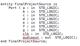
At this point, you are ready to begin the actual construction of the composer. The composer will need an entity, architecture, and two process blocks. The setup from step 2 will fill out the entity declaration for you. It should look like the first picture.
Now the fun part begins. Let’s begin by specifying the signals that we will use between the process blocks in the architecture. The following are the signals that will be used. The counter will help with the frequency division, the temp_out gives us a signal that we can hold a temporary value in, and note is used assign the note to be played. This should look like the second picture.
Following the begin is where we will place our process blocks. The above gives the signals and the architecture. The end of the architecture is specified by end my_project.
The Design


Next we need to begin the actual design of the composer. The first process block will function as a frequency divider. An example process declaration is as shown in picture 3.
We will now make use of the clock’s 50MHz signal for this. The idea is to increment counter until it reaches a threshold value and then toggle temp_out each time it hits this value. This will give us a lower slower frequency that represents a note’s frequency. For example, the note A is 440Hz. We can get this frequency from the clock by dividing 50MHz by 440Hz. We then take this value and when the counter reaches this value, we toggle temp_out, else we simply increment the counter.
Once we have divided the frequency into each of the given notes, we must check to see if a note’s corresponding switch is pressed. This is done by checking the value of note. If note is “000”, then the switch for note A is pressed. If note is “010”, then note C is pressed and so on.
Lastly, we need to ensure notes can only be played on the rising edge of clock. This is done by encasing it in an if statement that checks for a rising edge. It should look like picture 4.
Frequency Division
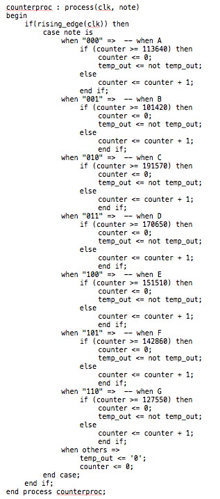

Now comes the implementation of the frequency divider. Since we have laid out all of the specifications, the rest is simply copying and pasting and covering all of the different possible conditions. Te entire frequency divider with all of the notes set up is provided in picture 5.
Notice how when note is “111”, we simply reset the counter and output to 0. This is because the board only plays seven notes and we don’t want any illegal values for unsupported switches. At this point we now need to store the value of temp_out for use with the speakers. This is done by assigning temp_out to audioout as shown in picture 6.
This will allow us to save the frequency we got from the previous process and actually use it.
Process Statements
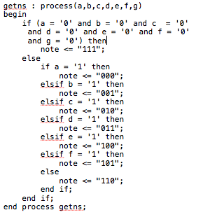

Now we proceed to designing and implementing the second process block. The second process block will handle getting the next state. To help with simplicity, we used states to represent each note. This state machine will allow us to set its state to each note we desire when its switch is toggled. For example, when the first switch is pressed, note A will be selected and be set as the next state, which will assign the value to the signal (from the architecture declaration’s) note. This will allow us to do our check in the first process block for which note to be played. An example declaration of the second process block with a sensitivity list is in picture 7.
Next, we specify all of the different possible conditions where each switch is pressed separately. We first need to check that none of the switches are pressed. If none of the switches are, then we set note to “111”, else when a switch is pressed, we change its corresponding letter value. For example, when the first switch is pressed, the signal a will get this value. Then inside getns, we assign note the value we check for in the frequency divider. The process block uses a number of if’s and elsif’s to account for the different possibilities. The completed process block is in picture 8.
Notice how we checked if none of the notes are pressed first. This will ensure that we only get valid values for note. As well as this, the if’s and elsif’s inside of the second else ensures that we don’t accidently assign note a value other than “111” when none of the supported switches are toggled.
Putting It All Together
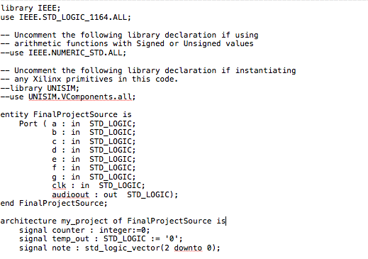
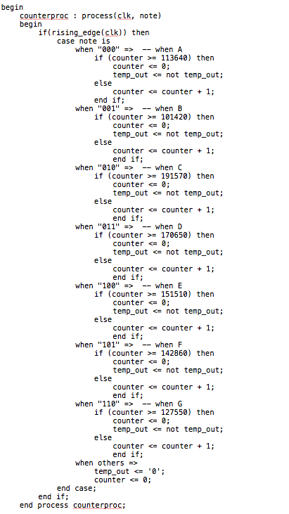
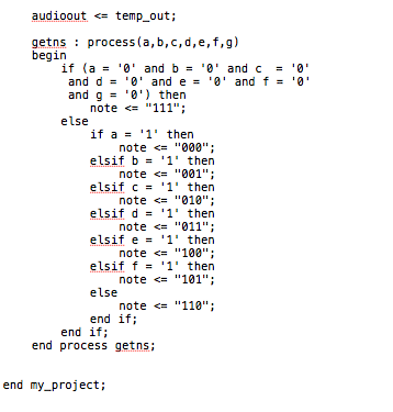
At this point, we are basically done. All that we need to do is assemble all of the VHDL and synthesize it. There should be no errors when synthesizing. After this, the expected source is in picture 9, 10 and 11.
Now the composer is complete. The next step is to test using stimuli to ensure that it actually works. Since this is not vital for the working of the composer, we do not explain testing here. Our test code is provided with the source code for this project.
Setting Port Maps
Almost there! Now all that we need to do is assign port values so that we can make the composer work on the nexys board. This is done by clicking on Plan Ahead. Once this application opens up there will be an interface with a weird looking board on it. From there we look at the bottom box, which contains the port maps for the entity values. From here, we assign each entity a port on the board corresponding to its correct switch. After this, we need to assign ports for the speaker’s wires. Once this is done, save and exit. Now we can synthesize again and click generate programming file. After this point, you will need to switch the startup option to JTAG Clock. This is done by clicking process at the top, then click properties. In the window that appears, select JTAG Clock under startup options (it is originally CCLK). Now, exit that window and generate the programming file again.
Programming the Board
Now, open Adept by Digilent and connect your board, making sure the board is on. Adept should automatically recognize the device. Now select the bit file in the browse window. Once selected, hit program. Now the board has been programmed. The next step is to wire up the speakers. This is done by connecting the wires to each of the ports that you selected in Plan Ahead. Then you’re done!
Have Fun!
Mess around with the composer and make the speakers play the different notes. Have fun!