Eagle Script to Prepare PCB Design for CNC
by mdeudon in Circuits > Electronics
1347 Views, 6 Favorites, 0 Comments
Eagle Script to Prepare PCB Design for CNC
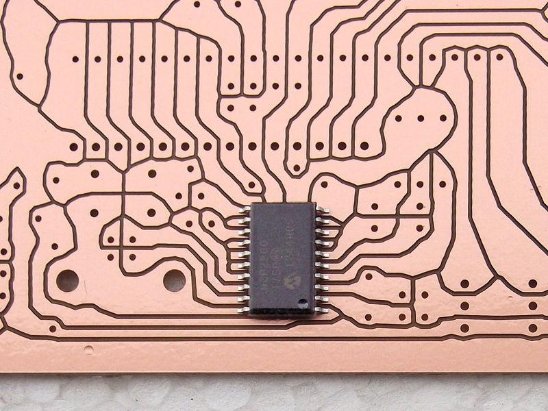
When using a CNC to produce Printed Circuits Boards, it is not always necessary to carve tracks and remove extra copper as with a photographic method.
Just separate each signal and make tracks as large as possible is faster and easier especially if your CNC is not 0.1mm accurate.
This method is also called 'Voronoïd', from the so named mathematician.
I want to share here a python script that draws automatically dots to help you to make separations on the copper layer.
Supplies
- Tested with Eagle 9.6.2 but should work for other vesion
- Python3 installed on your PC
- The eagle_cnc.py script
Downloads
Use the Script
We assume that your board is rectangular and one side only (TOP or BOTTOM it doesn't matter).
How to use the script :
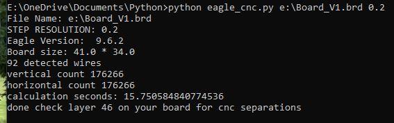
- python eagle_cnc.py <board path> <STEP>
- example : python eagle_cnc.py e:\board_v1.brd 0.1
What STEP means ?
STEP is the size of the grid used to make calculations (in mm or mil depending on the unit you choose for your board).
The thiner is the grid the better result you will have, but the longer the script will take to make calculation. For complex circuit, it can take few minutes, so be patient.
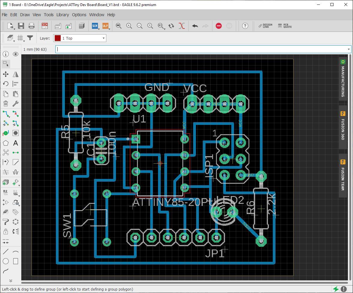
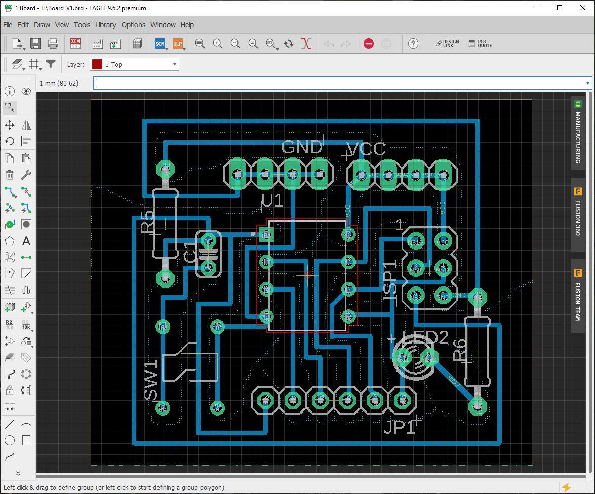
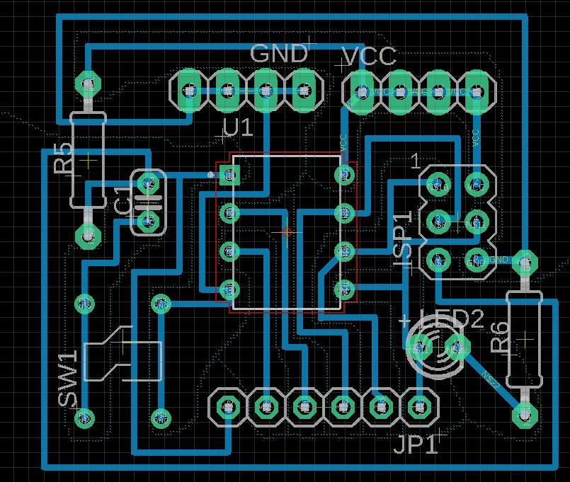
The script will modify the xml file containing your board (*.brd) adding dots on layer 46.
Draw Manually the Separations
What you need to do next is to draw separations yourself, just follow the dots
Then proceed with CNC. That's all !!
Example
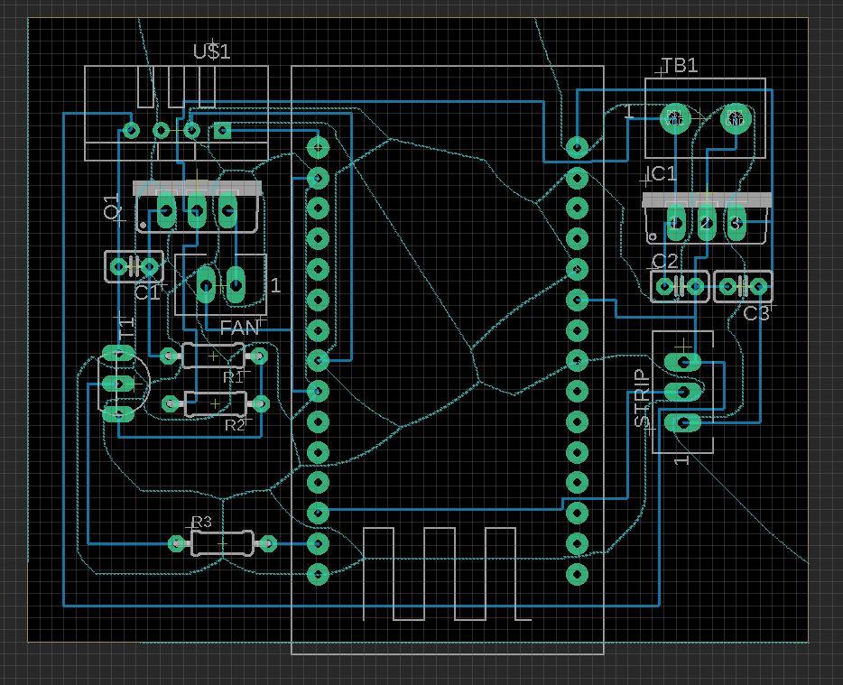
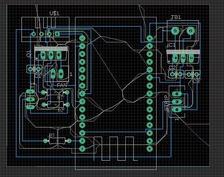
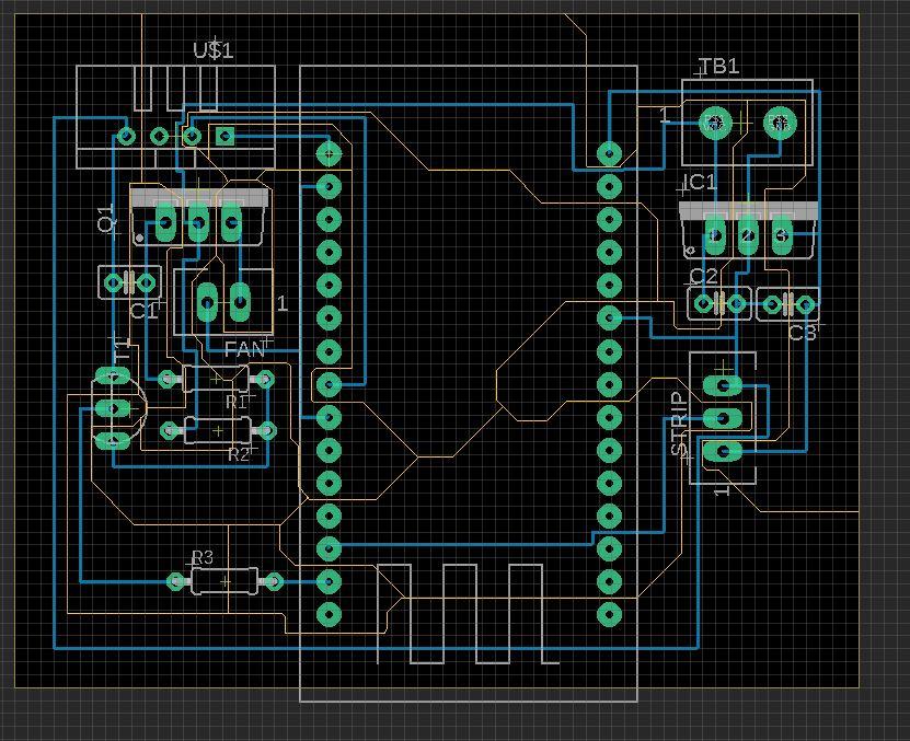
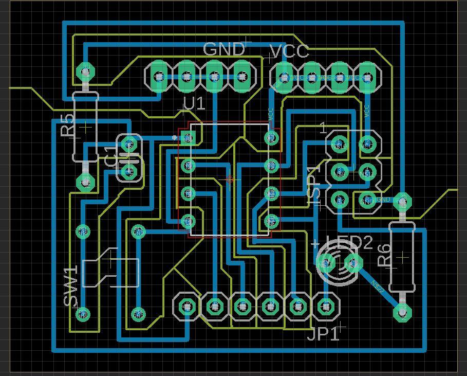
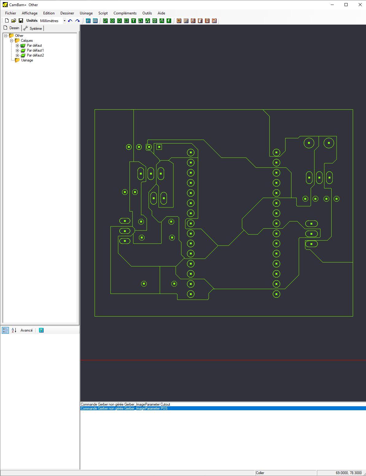
I've designed a simple board with an NodeMcu module, DHT11, connector etc ...
After applying my script, I can see my 'dot helpers' on the layer 46. Then I will use the layer 255 (routoute) do draw tracks seperations (see picture attached).
-> use a width = 0, this will help you for the cam processing
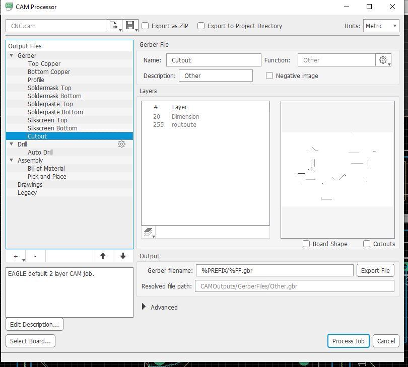
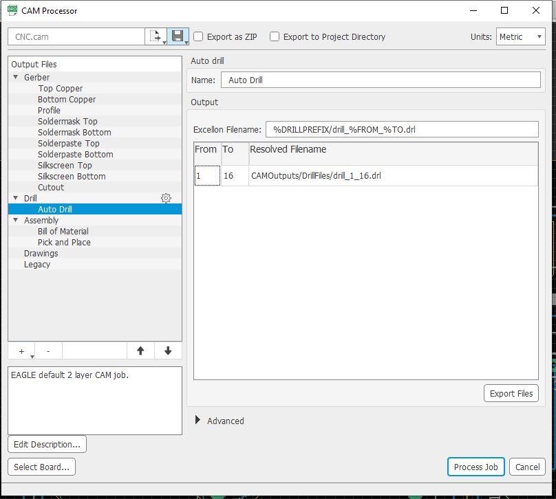
Export the Cam Files
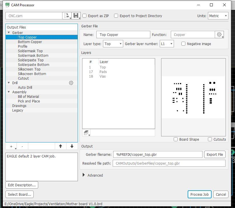
- Export the TOP COPPER layer
- Export layer 20 (dimension) and layer 255 (routoute)
- Export drill file
Cam Processing
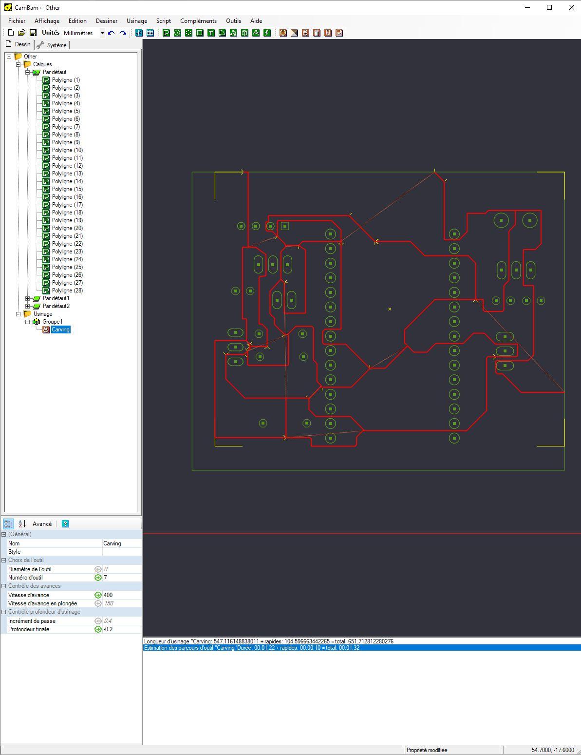
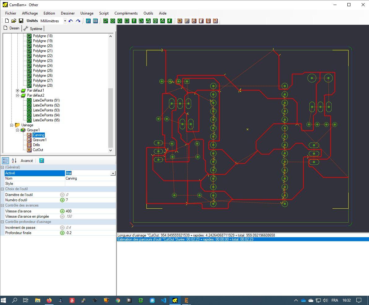
I will use CamBam to make the example. But of course this will work with another router software.
- Import gerbers files and drill file from above step.
- Set Up a carving operation for tracks separations. Personnaly I use a 60 °V-bit and a depth of 0.2mm.
- If you have setup the width of layer 255 to 0 in Eagle, you won't have to deal with the tickness of the lines.
- Take care of unconnected the pads : in my example I have pads which are connected to noting, so I need to carve arround to separate them from copper.
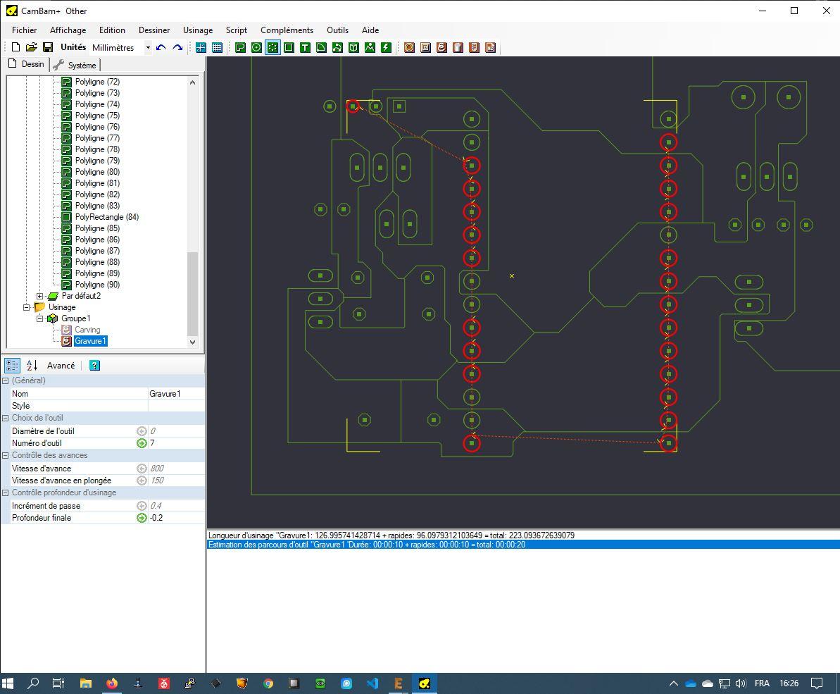
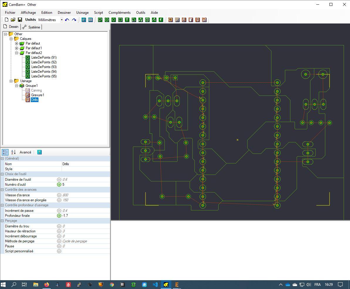
- Make the drill job.
- Make the cutout job.
Cam Result
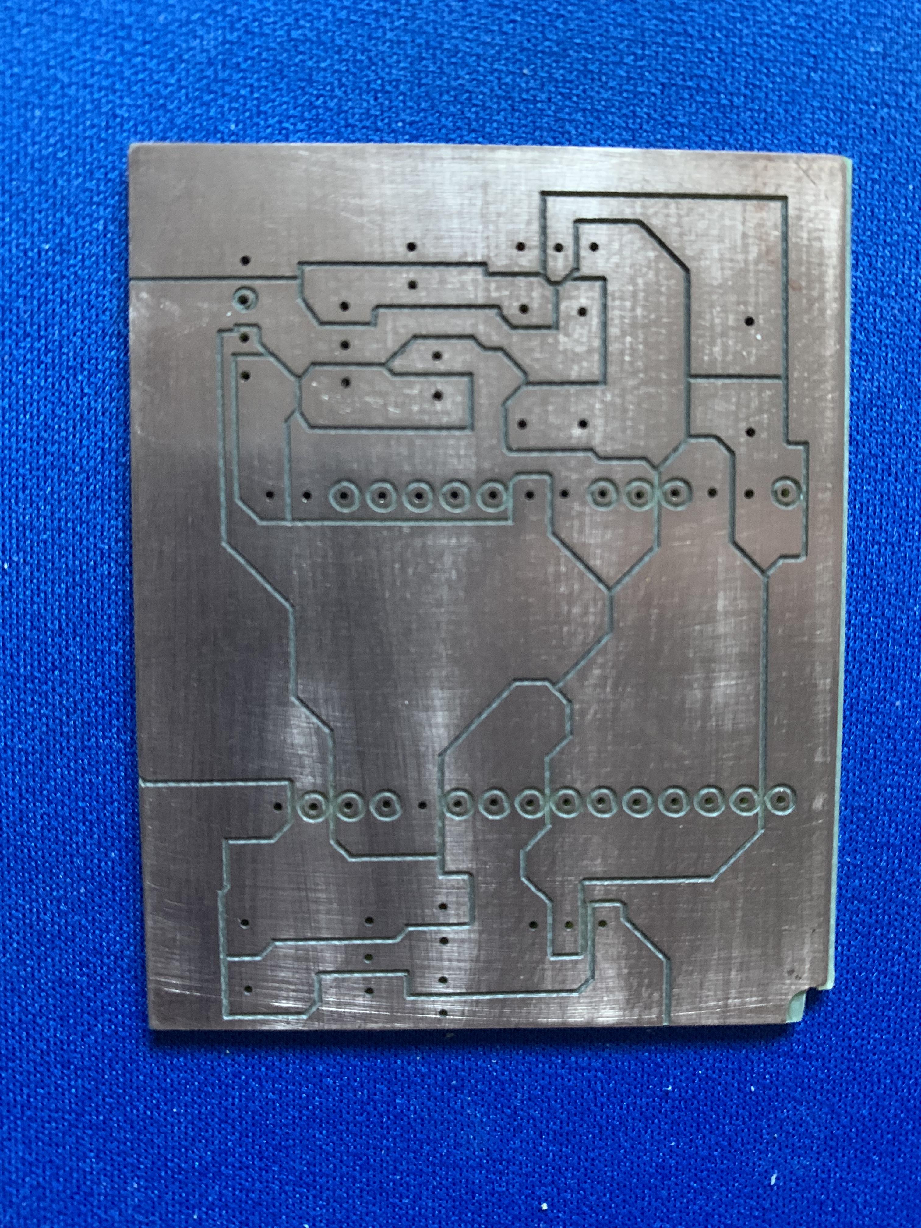
Don't forget to mirror the design before carving, because the components are place on the top.