Diy Arduino MEGA Simple
.png)
.png)
Starting with hardware, the Arduino Mega is based on the Atmega2560 microcontroller. In the iteration that is found on the Mega board, the microcontroller comes in a standard TQFP 100-pin package.
There are 54 standard GPIO available and a variety of peripherals including dedicated PWM channels, the typical serial interfaces like SPI and UART, and more.
It is a 5V microcontroller like the Uno, so your first step when transitioning this chip to a custom PCB should be to ensure that your board provides a 5V source to power the board.
Note that the microcontroller provides an AREF pin on pin 98 for the package above. This can be left floating or shorted with a capacitor to ground, since the microcontroller can source its own reference.
But if your application has particularly stringent analog performance requirements it is recommended to use a dedicated voltage reference chip.
This is an IC designed to provide a very stable, noise-free DC voltage source that does not need to provide very much current.
Supplies
.png)
.png)
.png)
.png)
This reference can and should be separate from the primary power supply, even if the voltages are the same. If your ADC requirements are not very strict, you can ignore this and simply tie the pin to a capacitor.

When it comes to the rest of the schematic, there is generally no reason to not reference the schematics for the official Arduino development board.
When first looking at the schematic what will stand out is that there seems to be two microcontrollers, a larger one on the left and a smaller one on the right.
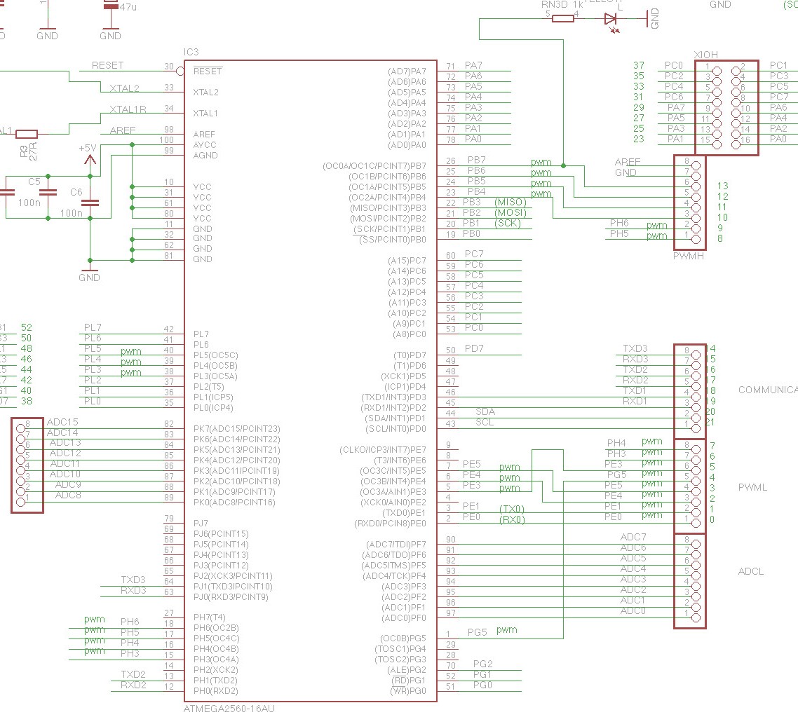 Figure 1- Schematic diagram for Atmega2560 core microcontroller circuit
The larger microcontroller is, of course, the Mega.
The smaller one, the Atmega8U2-MU, plays the role of USB-to-serial conversion, since the Atmega2560 does not have built-in USB functionality, only UART.
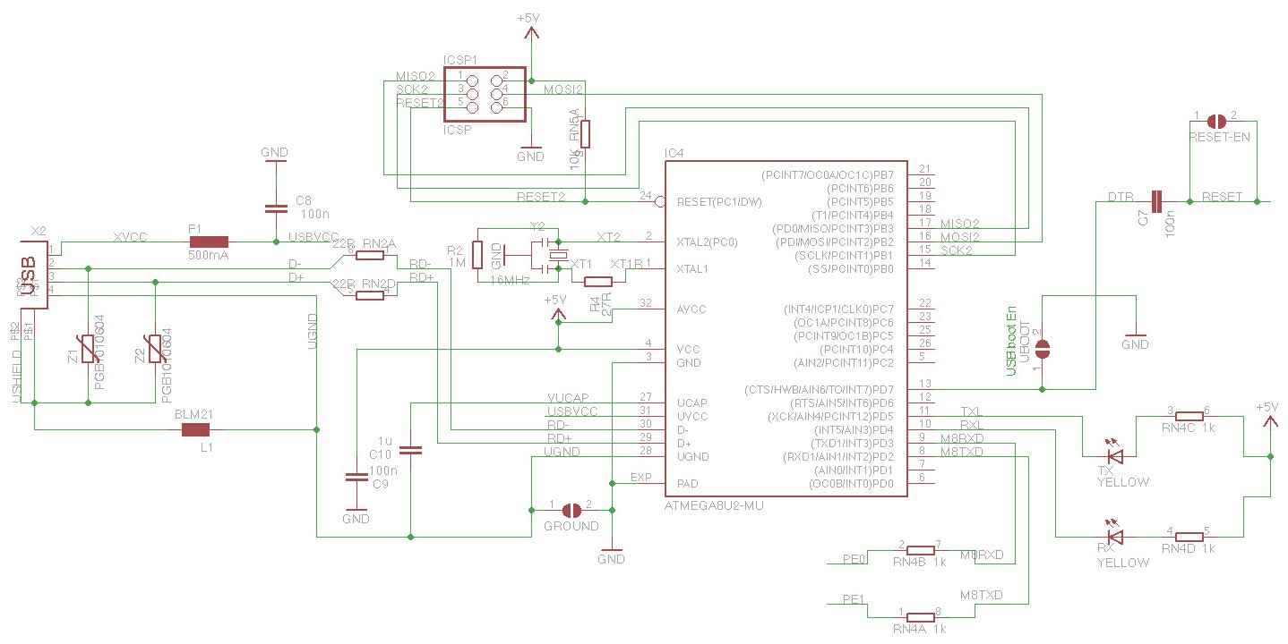 Figure 2 – Schematic diagram for Atmega8U2-MU USB-to-UART circuit
This brings us to a critical decision point in the hardware designing process; whether or not to retain USB functionality on the new manufacturable design.
The main argument against doing something like this is that if you are not using the USB functionality for something critical to your application (your device does not need to hook up to a PC for example), then including built-in USB connectivity is unnecessary.
It adds additional cost for the extra microcontroller and all of its required external components.
It also demands that a portion of the board edge must be clear for the USB port itself, which can be an issue in size-critical applications.
Programming interface (USB vs ICSP)
If you are freshly coming from dev-board Arduino programming, you may now be wondering how to program the board if there is no USB port.
After all, with the development board you just plug the computer into the USB port and upload code that way.
However, there is an alternate way to upload code to an Arduino board in the form of the 6-pin header labeled ‘ICSP’ on the dev board, with the same name in the schematic.
ICSP, or In-Circuit Serial Programming, is an SPI-style interface that requires an external programmer to upload code to the microcontroller. It is a lower-level way to upload code to an AVR microcontroller compared to USB.
ICSP is used by obtaining an external programmer like, and indicating in the Arduino IDE under Tools→Programmer what you are using. For this programmer, you would select AVR ISP.
From there you can write and upload Arduino code to the board as normal, as long as the programmer is connected on one end to your PC and the other end to the Arduino ICSP header.
ICSP is the ‘official’ way to upload code to the Atmega2560, so how does USB work?
This is accomplished via a bootloader, or a tiny program that controls the startup behavior of the firmware.
When this bootloader is ‘burned’ to a new Atmega2560 microcontroller using the ICSP, it essentially gains the ability to watch for and accept code uploads over another interface as well.
In the case of the Mega dev board, this interface is serial UART with an intermediary USB-to-UART converter to allow code uploads to be initiated and performed over USB.
The bootloader is designed to remain no matter what code is flashed over USB. It is easily burned using an ICSP programmer, by selecting the option Tools→Burn Bootloader in the Arduino IDE.
.png)
.png)
.png)
For a new custom PCB with an Atmega2560, at least the first code upload must be done with an ICSP programmer, since chips will not come from the factory with a bootloader.
Subsequent uploads may be done with an ICSP programmer as well, which is fully supported with the Arduino IDE.
There is not an explicit need to keep the USB port when transitioning to mass production
Should you wish to keep using the USB port for code uploads (essentially a ‘vanilla’ Arduino experience), simply burn the bootloader once using the ICSP programmer and then continue making code uploads over USB.
The USB-to-serial communication does not need to be done with a separate Arduino microcontroller as it appears on the Mega schematic.
There are a variety of dedicated ICs out there, most notably from FTDI, that perform UART-to-USB translation.
As long as your design utilizes the same TX/RX serial pins as the Mega dev board does (PE0 and PE0), your implementation should function largely the same.
Additional circuits
When it comes to the rest of the schematic, you can certainly just copy the circuit and IC item-by-item.
But, there are definitely a few parts you will want to strip away for a real product, most notably the pin header breakouts for all the GPIO.
Just leave the unused ones floating and only break out a small amount for debugging/emergency purposes.
Also note that the AREF pin in this schematic was left floating, but as mentioned above this can be tied to a stable voltage reference for precision analog purposes.
Finally, the Mega schematic depicts a voltage regulation block in the upper left corner that may be redundant in a custom board if you have already implemented a sufficient power solution.
Ordering PCB From JLCPCB


2 More Images
This project contains PCB and which was made with the help of JLCPCB
JLCPCB has upgraded the via-in-pad process of all 6-20 layer PCBs for free and provides free ENIG to make PCB products more stable and reliable. It is worth mentioning that due to large-scale production capabilities, JLCPCB is able to reduce the cost, allowing everyone to truly enjoy the benefits of the JLCPCB advanced fabrication. Here at JLCPCB, you can also get 1-8 layer PCBs at only $2
Go to JLCPCB website and create a free account.
Register and Login using Google Account is also possible.
Step 2 – Upload Gerber File
Once you have successfully created an account, Click on “Quote Now” and upload your Gerber File.
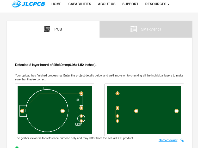
Gerber File contains information about your PCB such as PCB layout information, Layer information, spacing information, tracks to name a few.
Step 3 – Preview the File
Once the Gerber file is uploaded, it will show you a preview of your circuit board.
Make sure this is the PCB Layout of the board you want.
Step 4 – Choose Necessary PCB Options
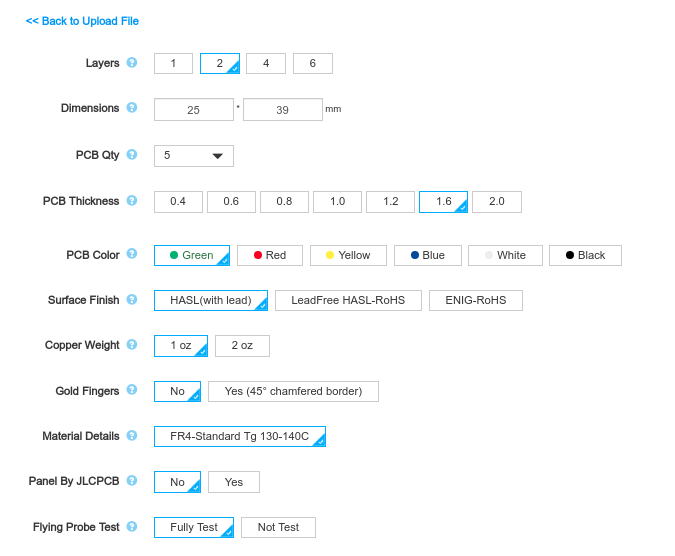
Below the PCB preview, you will see so many options such as PCB Quantity, Texture, Thickness, Color etc. Choose all that are necessary for you.
.png)
.png)
.png)
ICSP programming
The most obvious change will be required if the USB port is no longer used to upload code in favor of the ICSP programmer.
In this case, a codebase that makes liberal use of calls to Serial_println()will require adjustments, since the ‘default’ serial port (the same UART→USB pipeline used for programming) is no longer available.
This issue can be addressed in the hardware too, and has a few solutions:
1. Break out the UART interface to header pins, and use an external FTDI adapter like this one to read back those print statements when testing code.
If you use the same UART interface that is connected to the USB ports on the stock Mega, there shouldn’t be any firmware changes required.
2. Print to a separate UART interface. This requires a relatively small firmware change of simply adjusting the port that the Serial print library uses to write to.
Startup timing issues
Another change is more general and can apply to any microcontroller that is ported to a custom board: startup timing.
A common occurrence that can be missed on dev boards is that different capacitance values and different PCB layouts can cause the timing of startup events to change.
For example, if your custom power implementation has quite a large capacitance compared to the Mega dev board, or your PCB has very long traces coming off of the microcontroller GPIO pins.
This may cause cases in which the microcontroller takes longer to start up or a GPIO signal takes longer to stabilize.
In short, never assume that signals will retain their speed and integrity when switching to a custom board, and especially test code that runs right on startup to ensure it still runs properly.
One example of this is a microcontroller that reads the state of two GPIO pins that are pulled up to 5V (think a hardware ID) on startup.
If there is too much power supply capacitance, the microcontroller may be able to start up and begin executing code before the GPIO signals stabilize.
This may cause a bad reading of the pins, so you may need to add a startup delay to compensate for this extra stabilization time.
This is just one example of many of how subtle hardware changes can require steps to be taken in the firmware to correct.
.png)
.png)
Hidden features for external components
Another software change that may be required ties into the external component discussion from above.
When placing a part into a schematic when having previously just used the breakout board, you may note that there are interfaces available to the chip that were not utilized in your prototype.
Common examples of this may be an audio module having a dedicated reset button that was shorted out on a breakout board.
But now you have the option of tying it to your microcontroller GPIO and then issuing a reset via software.
Another example is perhaps a fault pin that is now available on a motor driver chip that wasn’t accessible on the dev board.
With the flexibility of a custom PCB comes new opportunities to interface with your peripherals, and this requires changes or considerations with the software as well as the hardware.
The design has a nice feature set:
- Power bus for +5V and GND down the center of the board.
- Central bus can be configured to carry +5V, GND, neither or both (set with jumpers)
- Special horizontal 5-pin bus to install pin headers for external connections
- 2x5 IDC connector area for external connections
- Holes connected in groups of five, much like a breadboard
- All regular Arduino pins accessible on top
- No worries about shorting against large USB jack! This Shield does not go over it!
- Power LED and reset button on top
- USB/External power jumper accessible with protoshield installed
Components required to fully populate the protoboard are:
- 0.1µF or 0.22µF capacitor
- 330/470 ohm resistor
- LED
- Tactile Switch
- Header pins (2x3 female, 6-pin female, 9 x 8-pin female, 6-pin male, 2 x jumpers)
.png)
.png)
Power
The Mega 2560 can be powered via the USB connection or with an external power supply. The power source is selected automatically.
External (non-USB) power can come either from an AC-to-DC adapter (wall-wart) or battery. The adapter can be connected by plugging a 2.1mm center-positive plug into the board's power jack. Leads from a battery can be inserted in the GND and Vin pin headers of the POWER connector.
The board can operate on an external supply of 6 to 20 volts. If supplied with less than 7V, however, the 5V pin may supply less than five volts and the board may become unstable. If using more than 12V, the voltage regulator may overheat and damage the board. The recommended range is 7 to 12 volts.
The power pins are as follows:
- Vin. The input voltage to the board when it's using an external power source (as opposed to 5 volts from the USB connection or other regulated power source). You can supply voltage through this pin, or, if supplying voltage via the power jack, access it through this pin.
- 5V. This pin outputs a regulated 5V from the regulator on the board. The board can be supplied with power either from the DC power jack (7 - 12V), the USB connector (5V), or the VIN pin of the board (7-12V). Supplying voltage via the 5V or 3.3V pins bypasses the regulator, and can damage your board. We don't advise it.
- 3V3. A 3.3 volt supply generated by the on-board regulator. Maximum current draw is 50 mA.
- GND. Ground pins.
- IOREF. This pin on the board provides the voltage reference with which the microcontroller operates. A properly configured shield can read the IOREF pin voltage and select the appropriate power source or enable voltage translators on the outputs for working with the 5V or 3.3V.
Memory
The ATmega2560 has 256 KB of flash memory for storing code (of which 8 KB is used for the bootloader), 8 KB of SRAM and 4 KB of EEPROM (which can be read and written with the EEPROM library).
Each of the 54 digital pins on the Mega can be used as an input or output, using pinMode(),digitalWrite(), and digitalRead() functions. They operate at 5 volts. Each pin can provide or receive 20 mA as recommended operating condition and has an internal pull-up resistor (disconnected by default) of 20-50 k ohm. A maximum of 40mA is the value that must not be exceeded to avoid permanent damage to the microcontroller.
In addition, some pins have specialized functions:
- Serial: 0 (RX) and 1 (TX); Serial 1: 19 (RX) and 18 (TX); Serial 2: 17 (RX) and 16 (TX); Serial 3: 15 (RX) and 14 (TX). Used to receive (RX) and transmit (TX) TTL serial data. Pins 0 and 1 are also connected to the corresponding pins of the ATmega16U2 USB-to-TTL Serial chip.
- External Interrupts: 2 (interrupt 0), 3 (interrupt 1), 18 (interrupt 5), 19 (interrupt 4), 20 (interrupt 3), and 21 (interrupt 2). These pins can be configured to trigger an interrupt on a low level, a rising or falling edge, or a change in level. See the attachInterrupt() function for details.
- PWM: 2 to 13 and 44 to 46. Provide 8-bit PWM output with the analogWrite() function.
- SPI: 50 (MISO), 51 (MOSI), 52 (SCK), 53 (SS). These pins support SPI communication using theSPI library. The SPI pins are also broken out on the ICSP header, which is physically compatible with the Arduino /Genuino Uno and the old Duemilanove and Diecimila Arduino boards.
- LED: 13. There is a built-in LED connected to digital pin 13. When the pin is HIGH value, the LED is on, when the pin is LOW, it's off.
- TWI: 20 (SDA) and 21 (SCL). Support TWI communication using the Wire library. Note that these pins are not in the same location as the TWI pins on the old Duemilanove or Diecimila Arduino boards.
See also the mapping Arduino Mega 2560 PIN diagram.
The Mega 2560 has 16 analog inputs, each of which provide 10 bits of resolution (i.e. 1024 different values). By default they measure from ground to 5 volts, though is it possible to change the upper end of their range using the AREF pin and analogReference() function.
There are a couple of other pins on the board:
- AREF. Reference voltage for the analog inputs. Used with analogReference().
- Reset. Bring this line LOW to reset the microcontroller. Typically used to add a reset button to shields which block the one on the board.
Communication
The Mega 2560 board has a number of facilities for communicating with a computer, another board, or other microcontrollers. The ATmega2560 provides four hardware UARTs for TTL (5V) serial communication. An ATmega16U2 (ATmega 8U2 on the revision 1 and revision 2 boards) on the board channels one of these over USB and provides a virtual com port to software on the computer (Windows machines will need a .inf file, but OSX and Linux machines will recognize the board as a COM port automatically. The Arduino Software (IDE) includes a serial monitor which allows simple textual data to be sent to and from the board. The RX and TX LEDs on the board will flash when data is being transmitted via the ATmega8U2/ATmega16U2 chip and USB connection to the computer (but not for serial communication on pins 0 and 1).
A SoftwareSerial library allows for serial communication on any of the Mega 2560's digital pins.
The Mega 2560 also supports TWI and SPI communication. The Arduino Software (IDE) includes a Wire library to simplify use of the TWI bus; see the documentation for details. For SPI communication, use the SPI library.
Physical Characteristics and Shield Compatibility
The maximum length and width of the Mega 2560 PCB are 4 and 2.1 inches respectively, with the USB connector and power jack extending beyond the former dimension. Three screw holes allow the board to be attached to a surface or case. Note that the distance between digital pins 7 and 8 is 160 mil (0.16"), not an even multiple of the 100 mil spacing of the other pins.
The Mega 2560 is designed to be compatible with most shields designed for the Uno and the older Diecimila or Duemilanove Arduino boards. Digital pins 0 to 13 (and the adjacent AREF and GND pins), analog inputs 0 to 5, the power header, and ICSP header are all in equivalent locations. Furthermore, the main UART (serial port) is located on the same pins (0 and 1), as are external interrupts 0 and 1 (pins 2 and 3 respectively). SPI is available through the ICSP header on both the Mega 2560 and Duemilanove / Diecimila boards. Please note that I2C is not located on the same pins on the Mega 2560 board (20 and 21) as the Duemilanove / Diecimila boards (analog inputs 4 and 5).
Automatic (Software) Reset
.png)
Automatic (Software) Reset
Rather then requiring a physical press of the reset button before an upload, the Mega 2560 is designed in a way that allows it to be reset by software running on a connected computer. One of the hardware flow control lines (DTR) of the ATmega8U2 is connected to the reset line of the ATmega2560 via a 100 nanofarad capacitor. When this line is asserted (taken low), the reset line drops long enough to reset the chip. The Arduino Software (IDE) uses this capability to allow you to upload code by simply pressing the upload button in the Arduino environment. This means that the bootloader can have a shorter timeout, as the lowering of DTR can be well-coordinated with the start of the upload.
This setup has other implications. When the Mega 2560 board is connected to either a computer running Mac OS X or Linux, it resets each time a connection is made to it from software (via USB). For the following half-second or so, the bootloader is running on the ATMega2560. While it is programmed to ignore malformed data (i.e. anything besides an upload of new code), it will intercept the first few bytes of data sent to the board after a connection is opened. If a sketch running on the board receives one-time configuration or other data when it first starts, make sure that the software with which it communicates waits a second after opening the connection and before sending this data.
The Mega 2560 board contains a trace that can be cut to disable the auto-reset. The pads on either side of the trace can be soldered together to re-enable it. It's labeled "RESET-EN". You may also be able to disable the auto-reset by connecting a 110 ohm resistor from 5V to the reset line