Digital Voltmeter PCB Board to Measure Voltages Accurately
by arshmah in Circuits > Electronics
1054 Views, 0 Favorites, 0 Comments
Digital Voltmeter PCB Board to Measure Voltages Accurately

.png)
A voltmeter to measure voltages in digital using ICL7107 to reduce human error.
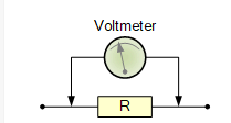
A voltmeter is an instrument that is used to measure the voltages(V) in an electronic circuit or a component. It can be defined as a potential difference between two points in a circuit.
There are two possible ways to measure Voltages.
- Analog
- Digital
Difference between Analog and Digital Voltmeter:
Analog Voltmeter:
These types of meters are also known as a galvanometer; they can be used to measure both current and voltages. It has a moving magnet coil that rotates when connected to an electrical circuit.
The analog voltmeter is not preferable to use because of its manual reading feature. The chances of errors while measuring voltages increases sometime the nob becomes slow while taking readings.
Digital Voltmeter:
Digital voltmeters are used to measure potentials between two different points and they display the values in the form of digits accurately that is why they are more reliable to use. The chances of making errors are less as compared to the analog voltmeter. They are more stable and provide a better interface to the user.
Supplies
Design Implementation
We are designing a circuit that will measure Voltages in Digital. All the inputs from those two potentials will be analog so we have to make all these values digital. We have many options to convert analog values to digital but we will use ICL7107 IC due to its functionality as it will convert Analog to Digital and also give us output for 7 segments which will be easy for us. ICL7107 IC will make outputs for 7 segments internally, we don’t need any additional circuit for 7 segment data converter.
Circuit Working
First of all, We need positive and negative voltages for our circuit. Negative will be supplied to ICL7107. We will make these negative voltages with the help of a timer IC. NE555 IC will be used in Astable mode(output oscillates at a particular frequency and generate pulses in the rectangular waveform). In Astable mode, 555 will provide us continuous voltage when it will be triggered. For positive we are using 7805 LDO. It will help us connect 9-12V as input of the circuit and provide us with a constant 5V positive for ICL7107 IC. Then, we need two potential differences on pins 31 and 35. After that, we have to make the internal clock circuit for ICL7107. R1 and C1 will be used for the frequency of the internal clock. Then, we have to connect outputs from ICL7107 with 7 segments. We are using common anode 7-segments and we will supply +5V to them then, We need to ground them or provide 0 to complete their circuit. So, ICL7107 will give 0 or ground to reference pins of 7-segments. As ICL7107 is making a decision on when to turn ON 7-Segments LEDs. 0 may vary for a different set of arrangements. Like if we have to display 1 on 7-segment we have to ground or provide 0 to B and C and it may vary for a different set of numbers that will be displayed.
Schematic File

I have implemented the schematic diagram of my design in Altium Designer. For the schematic, I have used the empty schematic file in an empty project. Using all the symbols and footprints which I have made in schematic and footprint libraries I have designed and connected the components. After creating the schematic, I have uploaded my schematic file online on Inventhub, users can view or download design files to implement my design.
PCB Design


After completing my schematic, I have converted my design into a PCB file where I can design my board and can view it in 3D. I have uploaded the PCB file on Inventhub where I can explore my design in different layers that will also help me in focusing on a specific layer of my board. I can view the previous changes I have made or the added or removed components in my design.
Components Management Libraries

Before implementing the design in the PCB file, I have created the symbol and footprint of each component. Then I have uploaded each symbol linked with their footprint on Inventhub. Each component is attached to its supply chain. While designing the PCB board it is important to take care of the footprint and dimensions of each component. Footprints should be exactly the same as per component size otherwise your design will not be perfect.
Release File

I have uploaded the release file of the design on Inventhub. This file contains all my design files in a ZIP file format. For fabrication instead of visiting the manufacturer, I will share my project files with him. The manufacturer only needs to export the file and he can fabricate the board without any error.
Project History Files

If I want to restore the previous version of my design and want to use it as my current design I can go to the revisions of my project where I have uploaded every edit of my design on Inventhub. I can easily go to the specific version of my design and can reuse it. The backup files of my design are available on Inventhub for the users.
BOM File

After getting the fabricated board I can embed components on it. For this, I have created a Bill of Material on Inventhub which consists of all my component details with manufacturer and supplier details. My component provider can export the file in CSV format and can deliver my components. My total cost of the components is also being calculated automatically as per my choice of distributor and quantity. For this project, my cost for the components as per my BOM details is $21.499 which is affordable.