Design a Romantic PCB Using a Free PCB Design Tool - EasyEDA
by vividz in Circuits > Electronics
9311 Views, 109 Favorites, 0 Comments
Design a Romantic PCB Using a Free PCB Design Tool - EasyEDA
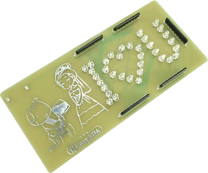
Have you ever tried to design a PCB for your lover or children or friends on a special day? Why not?
PCB also could be an amazing gift which reveals your creativity also hones your PCB skills. Here I’d like to share a Romantic PCB designed using EasyEDA. It is a free, web-based and easy-to-use EDA tool integrating powerful circuit design, mixed-mode circuit simulator and PCB design.It is developed to give engineers, students and hobbyists an Easier EDA Experience.
Design a Romantic PCB With Flash LED
How to Design a Romantic PCB
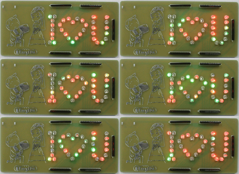.gif)
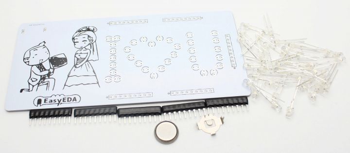
This romantic LED board consists of 35 Flash LEDs and a CR1220 battery cell and of course some resistors to limit the flow of current. Since this circuit is no more than 35 LED’s and resistor arrays even beginners can try this PCB out and make a beautiful gift.
ROMANTIC PCB CIRCUIT DIAGRAM:
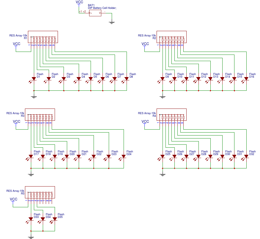
This is the circuit diagram of this Romantic PCB as you can see there is nothing more than LED’s and current limiting resistors. I have used Resistor array packages in my circuit for making it simple and keep the space minimal.
TO DRAW a NEW SCHEMATIC DIAGRAM:
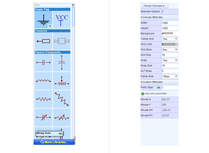
First you need to create an account in EasyEDA, its totally free of cost. Then go for a “New project” and you will see a workspace opening up for you where you can draw your own circuit diagram in it. You can search or browse through the parts required using the menu provided in the left side of your workspace. And the attributes of our workspace can be modified using the attribute pane located in the right side of the workspace. Please see attached Snaps for reference.
Once you finish your circuit, run your design and see if you get any errors.
Save your project and your schematic is done now. You can access the schematic diagram of this romantic PCB through this link https://easyeda.com/editor#id=XVd7NHmgW|MOI0UcuoG
CONVERTING YOUR SCHEMATIC TO PCB:
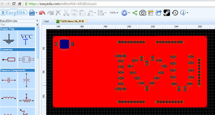
Now you can click on the button Convert to PCB in the top menu to get the PCB version of your schematic. You will get a pre designed version of PCB, you can modify the layers, change the positions and tweaks you need to do. After doing this i have obtained a final output something like this.
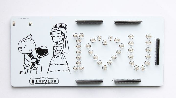
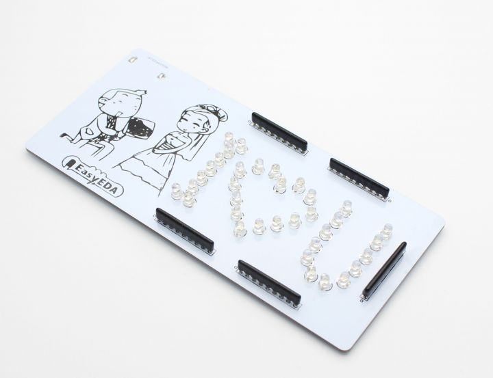
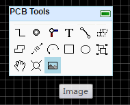
I have placed the LED’s placing in the pattern spelling that “I Love(heart) You”. Cool isn’t it? Now lets make this thing even cooler by adding a image of your choice to this PCB. To do this click the ‘image’ button in the PCB Tools menu on EasyEDA, and select an image in the new window of ‘Insert Image to PCB’.
Insert Image to Make the PCB Romantic
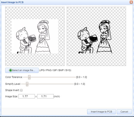
Also, you can use Color Tolerance or Simplify Level function to adjust your image.
After completing the above steps, you could press the button ‘Insert Image to PCB’, then you will see your image that have been already inserted to PCB. Finally your design will look something like this below.
Edit the PCB
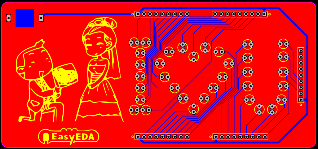
Next, move the inserted image to the left of PCB, you can see and edit it online at
https://easyeda.com/editor#id=XVd7NHmgW|MOI0UcuoG
Of course, you can change the layer you like and insert the image you like.
Access the PCB Design of This Romantic PCB Board
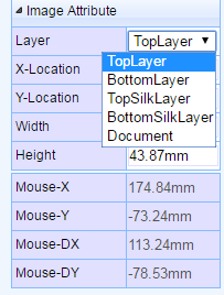
If you decide to choose a new layer, you set the attributes using the pane located in right side of the workspace.
You can access the PCB design of this Romantic PCB board through this link
Design a romantic PCB with flash LED
Order This Romantic PCB Directly From EasyEDA
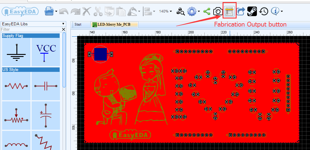
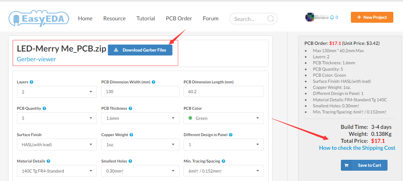
If you are using EasyEDA online cad tool, then it would simply be a matter of a few clicks to get your design into production. Just click the “Fabrication Output” button then you will be redirected to PCB order page, fill in your details and you will get the PCB delivered directly. In that page you can place an order quickly and easily, you will get your PCBs a few days later.
You can directly order this "I♡U" board or download the Gerber file using this link.
How to Make a PCB at EasyEDA

Well it’s impossible to finish the how to use tutorial in a single article.
So here is a tutorial repository that will teach you to use this design platform more effectively. Hope you like this article and would like to give EasyEDA a try, Happy Designing.
The following Youtube video from provides a quick review of EasyEDA features.