Design a Prototype PCB in Altium Designer
by taste_the_code in Design > Software
840 Views, 2 Favorites, 0 Comments
Design a Prototype PCB in Altium Designer


I very often use electrical boxes in my projects as enclosures, so I decided to design a custom PCB that will fit in those boxes and serve as a base for future projects.
In this tutorial, I will guide you through the process of creating a custom printed circuit board (PCB) using Altium Designer and ordering the PCBs from PCBWay. We will cover the necessary steps from defining the board outline to adding mounting holes and prototyping pads.
Supplies
Before starting the project, you will need access to a computer with Altium Designer installed and an internet connection. You can get a free trial of Altium and a 25% discount on any license on this link.
You will also need an account with PCBWay to order your PCBs. Following this link will give you a $5 welcome bonus so you can order your first boards for free!
The final PCBs will often be combined with these modules and sensors:
- ESP32 - https://s.click.aliexpress.com/e/_DEhchU9
- Arduino Nano - https://s.click.aliexpress.com/e/_DF4ak1L
- NodeMCU - https://s.click.aliexpress.com/e/_DDJaExB
- 5V relay - https://s.click.aliexpress.com/e/_DmuAJyV
- DHT22 Sensor - https://s.click.aliexpress.com/e/_DlczVdr
- TP4056 - https://s.click.aliexpress.com/e/_DFfG8t7
- Soil Moisture sensor - https://s.click.aliexpress.com/e/_DlGPB5R
- DS18B20 - https://s.click.aliexpress.com/e/_DnDGUMh
Creating a Paper Template

Since I wanted to be sure of the PCB size and shape, I first started the process by creating a template for it out of cardboard.
This template is shaped in such a way that it clears the mounting pillars in the edges of both style boxes and it is a bit smaller than the internal space of the box so it can clear out some passing wires.
Once I was happy with the template, I used it for the final PCB dimensions.
Create the Project From Altium 365


To create a PCB project from Altium 365, you must log in to your Altium 365 account, click on the "Create" button, and select "PCB Project" from the drop-down menu. Afterward, you will be redirected to the Altium Designer interface, where you can begin your PCB design.
By creating your project this way, you automatically have the project set with version control so you can safely store it online and come back to make revisions when necessary.
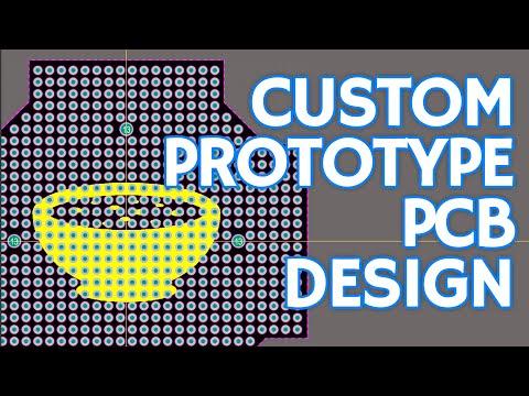
Define the Board Outline


One of the critical steps in creating a PCB project is defining the board's outline.
The board outline is the physical dimensions and shape of the PCB. Since I'm basing mine off the template that I previously created, I first draw a rectangle and then added the corner cutouts.
To modify the shape, you need to reduce the rectangle as a polygon so you can trim off the corners.
Once you are happy with the shape, you can set it as the board outline.
Add the Prototyping Pads


Since this will be a general-purpose PCB, I want to have as many pads as possible so I set the snapping grid in Altium to 100 mil (2.54mm) which is the most common pin spacing and I started adding pads to the board.
To add prototyping pads to your PCB design, click on the "Pad" tool, and draw the pads onto the PCB. You can customize the pad's size and shape to suit your needs.
Add Mounting Holes


Mounting holes are holes that allow you to attach the PCB to the enclosure.
To add them, I simply used pads that I first enlarged so a screw can pass through them. The placement is defined by the mounting pillars on the electrical box, which in my case were in the center in a cross pattern.
Order the PCBs From PCBWay


After completing your PCB design, the next step is to order the PCBs from a manufacturer.
PCBWay is an excellent option for ordering PCBs, as they offer high-quality PCBs at an affordable price. To order PCBs from PCBWay, export your PCB design to Gerber format, navigate to the PCBWay website, and upload your Gerber files.
PCBWay will then manufacture and deliver the PCBs to your desired location.
You can get the Gerber files and order the PCB from here.
With the boards designed and off to manufacturing, I can now start to think about the projects I'll use them for.
To stay tuned for that, make sure to subscribe to my YouTube channel, and also check out some of my other Instructables.