DIY Bluetooth-Controlled Car/Robot
by GreenPAK™ in Circuits > Robots
19 Views, 0 Favorites, 0 Comments
DIY Bluetooth-Controlled Car/Robot
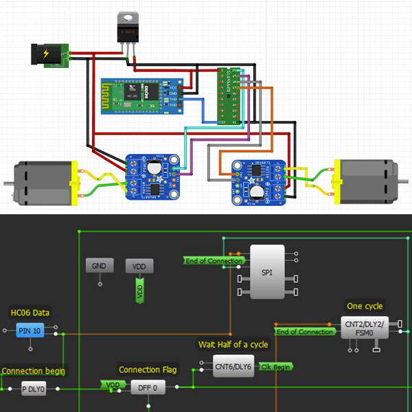
This Instructable shows how to make a car/robot controller with Bluetooth and an Android app. It is all done using an SLG46620V GreenPAK™ IC, HC06 Bluetooth module, motor drivers, and motors. First, a simple android application was developed to send signals to the Bluetooth module, which in turn sends data to the SLG46620V. The motor is directed by processing the data with SLG46620V.
This project contains 3 stages :
- Android Application
- Retrieving data coming from the Bluetooth module
- Controlling the motors
Below we described the steps needed to understand how to program this device. However, if you just want to get the result of programming, download GreenPAK Designer software (a part of the Go Configure Software Hub) to view the already completed GreenPAK design file. Plug the GreenPAK Development Kit to your computer and hit the program to create the system.
Android Application


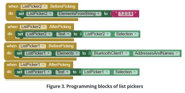
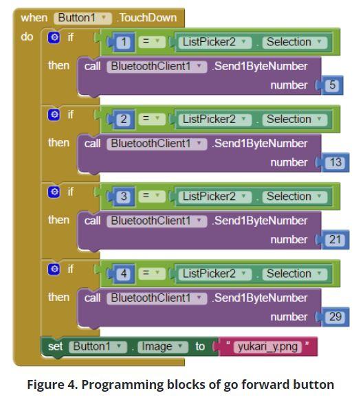
In the first stage, we will compose an application for android devices to send data to the Bluetooth module. MIT app inventor 2 website was used to compose the application. On this website, you can easily create an application with programming blocks, without any programming knowledge. Meanwhile, let’s think out what kind of data will be sent to the Bluetooth device before programming and designing.
Common directions a car basically moves in are left, right, forward and backward. To specify 4 different actions, 2 bits are enough (Table 1). After having specified car directional moves, let’s set the speed of the car.
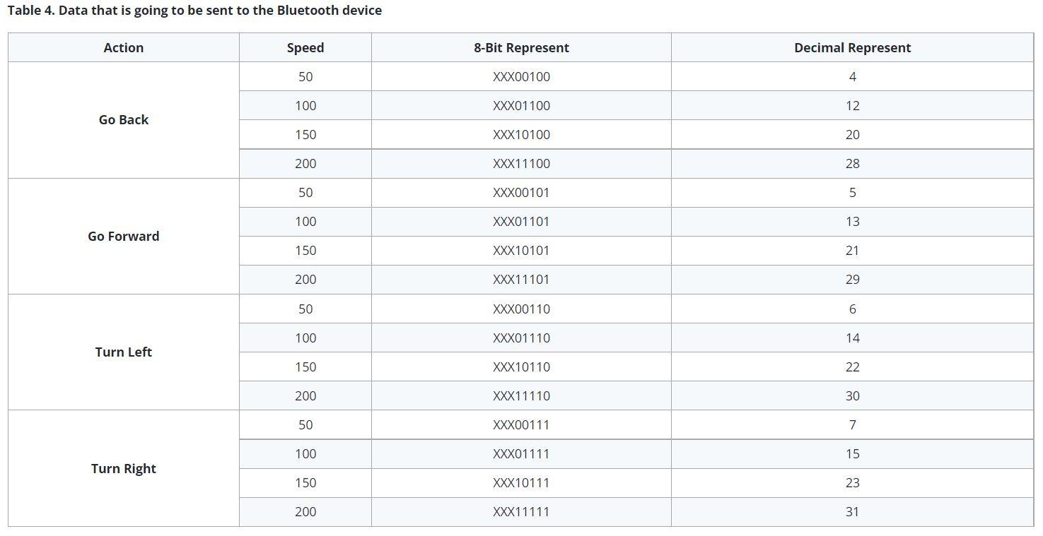
Because there are 4 different registers in the PWM0 block of the SLG46620V IC, we can adjust the speed to 4 different settings, and 2 binary bits are enough for this (Table 2). Examples of direction are shown in Table 1, examples of speed, on the other hand, are shown in Table 2. The data is sent to the Bluetooth module as 8 bit packages, and 5-bit data is enough for us. We can ignore the remaining 3 bits. We may align data as in Table 3. According to this bit sequence, the calculation of data that needs to be sent is as shown in Table 4.
Now we are able to create the application regarding these calculations.
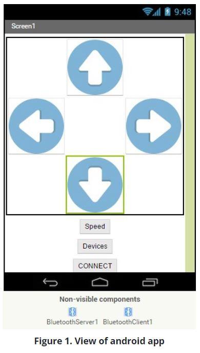
Four buttons to define rotations, a list picker for devices and speed control, and a button for connection is enough. Also, we have to add a Bluetooth client and Bluetooth server module to make a Bluetooth connection. To see directional buttons aligned, use the table arrangement. The design is shown in Figure 1.
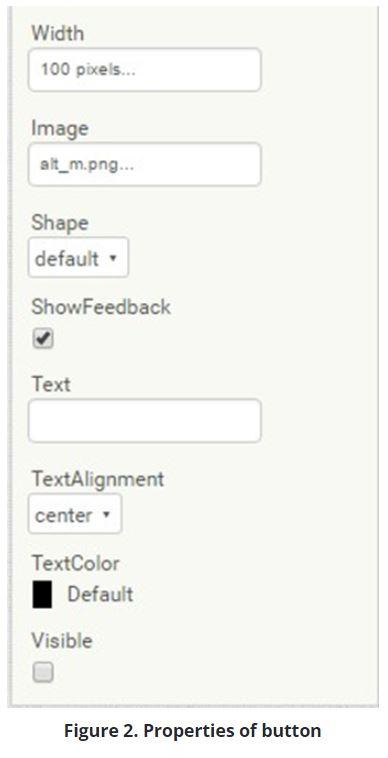
In the first opening of the application, remove the visible tick of the remaining content one by one which is located in the properties section (Figures 2-4).
If you want to add figures instead of buttons, you can do this in the image section.
After designing, we pass programming by clicking the block section. Programming is quite easy with using Mix Application Inverter 2. You may add the block that you need by clicking components on the left side. In this part, we fill out the contents of the list pickers, and then line up the Bluetooth devices so that the former match the devices, therefore, we arrange the numbers as ' 1, 2, 3, 4 ' for speed.
You can find the project of this Android Application in the files that you have downloaded for this project. If you select 'import project from my computer' by selecting the project button located in the upper left, you can easily add the programs that you have made for your project.
Note: Some blocks are formed but are collapsed. You can right-click on them and investigate by clicking expand button.
Getting Data From Bluetooth Module

HC06 module that we use for Bluetooth communication uses UART for communication protocol.
A UART or Universal Asynchronous Receiver / Transmitter is a piece of computer hardware that translates data between parallel and serial forms. It is an integrated circuit used for serial communication that contains a receiver (serial to parallel converter) and transmitter (parallel to serial converter) each clocked separately.
Data Framing
The idle, no data state is high-voltage or powered. Each character is sent as a logic low start bit, a configurable number of data bits, and one or more logic stop bits.
HC06 sends 1 start bit, 8 data bit, and 1 stop bit by default, and also it has a 9600 baud rate. SLG46620V has an SPI block. We are going to make some additions to the SPI blocks which allow getting data that comes from the HC06 module. Initially, an external clock is needed for SPI protocol. However, data comes at a constant rate under the UART protocol. Another difference is that there is no start or stop bits in SPI communication. We are going to use a start bit to get the SPI clock going.
UART protocol is in a high power state when idle, and it passes to a low power state when it starts communication (start bit - low).
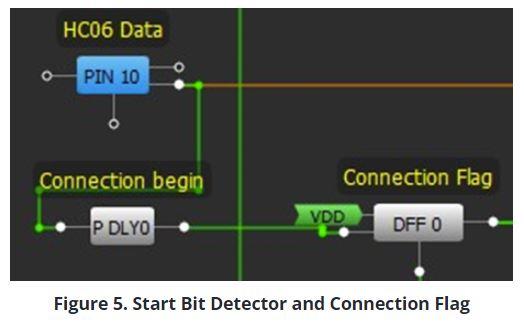
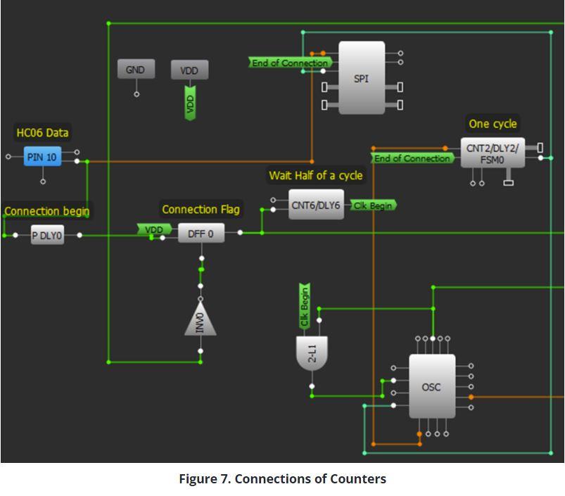
Therefore, we can use the Falling Edge Detector to identify the start of communication. We connected this signal to the clock pin of a DFF and VDD to the data pin for the connection to stay active during the connection.
Thus, the PDLY0 block is going to set the connection flag by catching the falling edge when communication starts. UART protocol has a 9600 baud rate which means it is able to transfer 9600 bits per second. To find the period of one cycle, you have to divide 1 second by 9600.
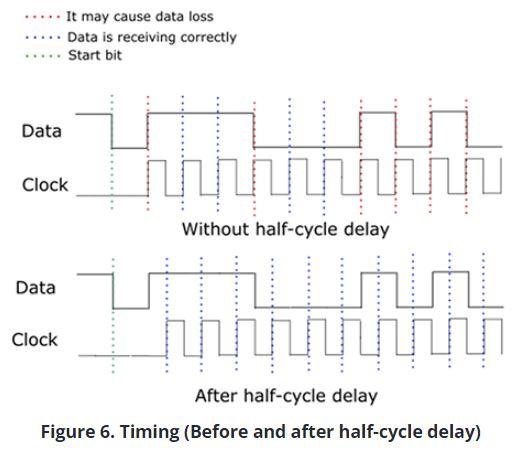
If you start the clock running immediately, data and clock signals will be changed at the same time and it may cause data loss. That is why the clock signal must be delayed for a half cycle. You can better understand the necessity of this by referring to Figure 6.
We applied this delay using CNT6/DLY6 block. We attained a higher frequency by setting the RC OSC Frequency from the OSC block as 2000 kHz. The cycles from which we attain higher frequencies have shorter periods, and the absolute timing resolution of the counter increases. Thus, we decrease the counter's error ratio.
Note: The counters in the SLG46620V chip have +/- 1 error ratio. While the error ratio is 0,04 ms at 25 kHz, it is decreased to 0,0005 ms at 2000 kHz.
CNT6 block is set in a way that it delays half a cycle (0,1042/2=0,0520 ms).
We used another counter (CNT2) to obtain a cycle's duration (0,142 ms). We set this counter's clock as External Clock0. By applying logic and process, we connected the OUT1 signal that comes from OSC and CLK BEGIN signal to OSC's External Clock0 input.
Thus, CNT2 will begin counting only when the connection starts. To give more detail, the counter-blocks count the edges of the clock signals.
If the counter constantly sends high or low signals to the CLK pin, the counter stops counting. Here, we AND’d CLK Begin signal with OUT1 signal and connected them to the External CLK0 input. In this way, at the moment when there is no connection, ANDing CLK Begin signal and OUT1 signal will always equal to 0 and CNT2 will stop counting.
But when the connection is provided, CLK Begin signal will be "1", the result of the logic and operation will be OUT1 signal and it will have CNT2 keep counting. We connected the output of the CNT2 counter (its cycle duration was calculated beforehand) to the SCLK pin of the SPI block. Hence, we generated a clock cycle for every byte of data coming from HC06.
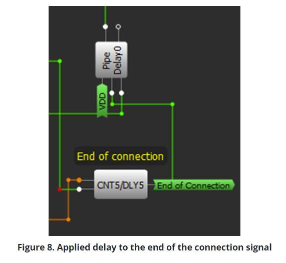
Finally, we set a delay in order to calculate the connection's expiration and to zero the connection. This counter will begin measuring the duration as soon as the connection starts and will end the connection when the data delivery is completed. We know that the data coming from HCO6 is 10 bytes (1-byte start, 8 bytes data, 1 byte stop). We zeroed the connection after measuring the duration of 9 bytes. Zeroing the connection during the stop byte makes the SPI block ready before a new connection is formed.
Otherwise, if it is intended to be zeroed at the end of the duration of 10 bytes, there is the possibility of failure to capture the start byte for the new connection.
We reset the signal coming from the out pin of the PLY5 block, SPI block, the counter with 1 cycle duration we had calculated as well as DFF0 which we use as the connection flag.
However, unlike the other ones, we delayed the signal a little before resetting DFF0. If you reset the counter-delay blocks of the SLG46620V chip, the out chip of the block remains high for 1 cycle.
If you reset CNT2 and DFF0 at the same time, the CLK Begin signal remains low, as a result of which stop CNT2's clock stops. As CNT2 will remain high for 1 cycle and the clock will shift to low status constantly, CNT2 will not be able to complete 1 cycle and will steadily remain in high status. Therefore, we reset the CNT2 block first and then DFF0 after a few cycles.
Control of the Motors/Car


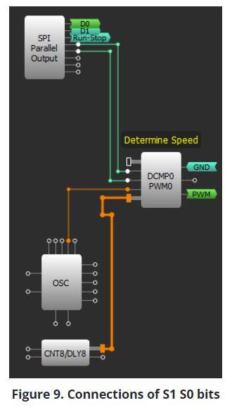


At this stage, we change the car's speed and direction by changing the outputs of the DC motors. The car's direction and speed information is received via Bluetooth. As we receive the data coming through the UART protocol via SPI block, SPI Parallel Output block will be used here. Let's remember the Data Pattern which we previously used to control the vehicle.
One of the differences between the UART and SPI communication is the sequence in which the bytes are sent. While MSB (Most Significant Bit) is sent initially with SPI protocol, it is sent last with UART protocol. Therefore, we will receive the bytes of the data with a reversed sequence.
The S1 and S0 bytes are the bytes by which we change the speed of the vehicle. So, we linked these bytes to the PWM0 block.
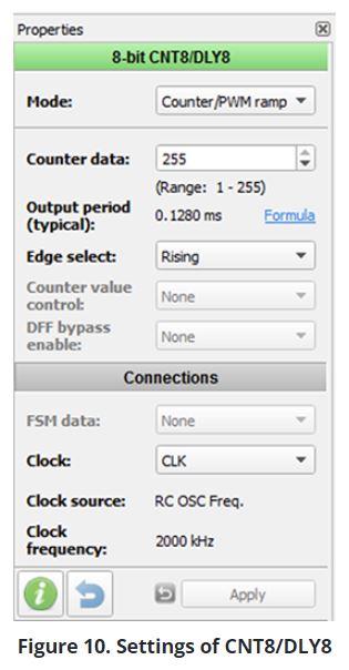
After the settings of PWM0 are applied as indicated above, the CNT8/DLY8 block is configured as indicated below.
Now, we are able to receive the PWM signal from the PWM0 block and adjust the signals necessary to set the car in motion. The SLG46620V IC cannot drive the DC motors directly. Therefore, we will be using a power supply and motor driver to control them. DC motor drivers run the motor by energizing the pins of the motor in accordance with the control pins that are usually named M1-A, M1-B, M2-A, and M2-B.
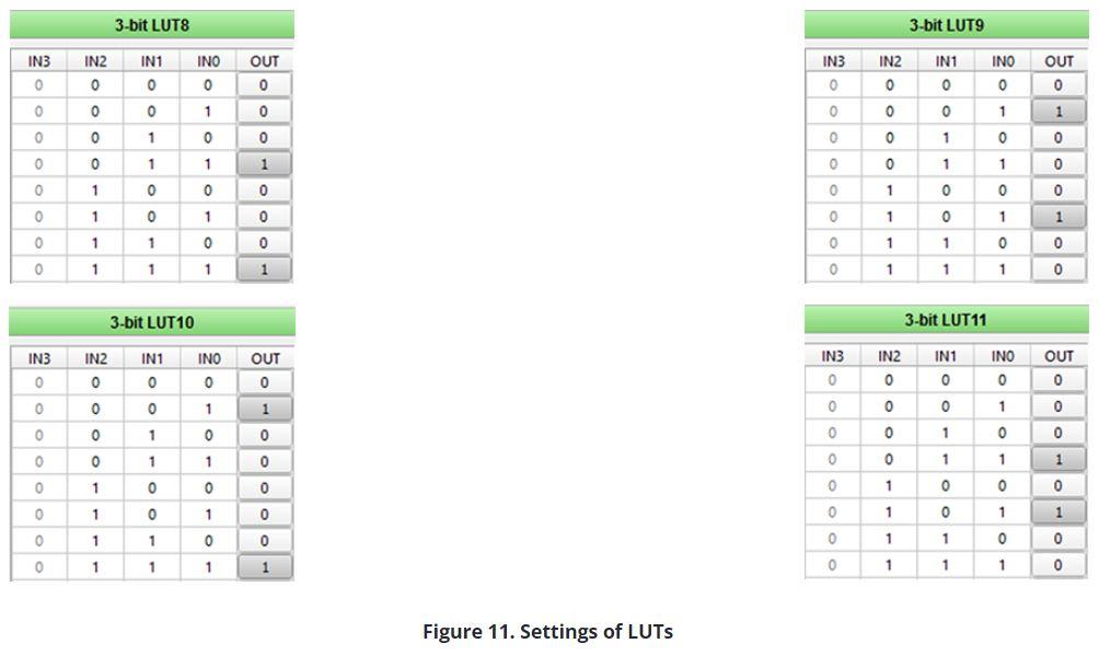
We build a connection in our design as shown in Table 8. The signals that must be delivered to the DC motor control pins in accordance with the D1 and D0 signals are as shown in Table 9.
According to this table, the settings of the LUTs that control the motor out pins must be as displayed in Figure 11.
Finally, the LUTs supply the proper logic signals to the motor driver inputs. Thus, the motor out pins will remain low while the open-close signal is in the low state and the motors will not rotate.
Top Level Schematic
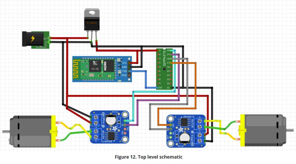
You can arrange the connections of the Bluetooth-Controlled Car as shown in Figure 12 attached to the above step. Since data only goes in one direction from the HC06 Bluetooth Module, we can just connect the Tx Pin. An engine drive card that can run two DC motors can be used instead of 2 motor driver cards. Also, it would be useful to use a voltage regulator in order to protect the IC and HC06 Bluetooth Module from high voltage.
Conclusion
In this Instructable, control data was sent to the SLG46620V IC and operated wirelessly via Bluetooth. The GreenPAK IC was successfully configured to support the UART protocol in data sequence and synchronization. Additionally, it can be synchronized with many sensors that use UART. This allows great flexibility in designing with Dialog’s GreenPAK IC for controls using smart devices (cell phones, tablets, etc.).