Printed Circut Boards - Complete Process
by Souperman2 in Circuits > Electronics
5416 Views, 22 Favorites, 0 Comments
Printed Circut Boards - Complete Process

The following describes the process by which I create PC circuit boards for one-offs and prototype use. It is written for a person who has created their own boards in the past and is familiar with the general process.
All of my steps may not be optimal for your situation. I have developed this process by trial and error incorporating techniques from various sources. Please take whatever works for you and discard that which does not.
A production note: I am old school and learn best from written instruction and pictures, they form the bulk of this instructable, I have included a couple of videos for some of the more complex steps.
Materials Needed
The following list is lengthy but, if you are already making your own PC boards, you may have some of these items. Most of the rest, with the exception of the UV exposure Box, can be purchased on-line.
You will need:
- Copper clad PCB material
- Circuit board design software (I use Eagle freeware).
- Gerber file translator - convert Gerber files to graphic format Gerber2PDF
- Graphics editing software (PhotoShop)
- Laser Printer w toner suitable for toner transfer technique.
- Glossy laser printer paper (Staples #633215).
- Transparency film for Laser Printers (C-Line no60837).
- Water soluble glue stick, cyanoacrylate glue, painters tape.
- Thin floral wire (~ 26 gage) and straight pins.
- Hand tools to cut, shape and drill PC boards.
- A standard clothes Iron.
- Circuit board cleaning materials ( paper towels, sponges, detergent, Bar Keepers Friend, solvents).
- Ferric Chloride liquid (40%).
- Citric Acid, powdered (nuts.com).
- Old CrockPot w/ ceramic or glass liner (not metal).
- Qt. size plastic Freezer bag with zip closure.
- UV curable solder mask paint (ebay or amazon).
- UV exposure Box (Home-Made?).
Design Your Circuit Board
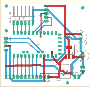
I use the Eagle free ware version since board sizes are fairly modest and limited to 2 sides. I am generous with the sizes of my traces and the distances between them ( 24 mil min trace size and 15 mil between).
Most of my components are through the hole but I do use SMD or a combination occasionally. I try to route traces to any pin headers on the bottom of the board. I do not use plated through holes so I add additional vias connecting the top traces to the bottom where component cannot be soldered on both sides. These will be filled with short pieces of thin wire soldered in place.
When I am finished with the layout and routing, I add several large vias near the corners of the board to serve as mounting holes and registration indicators for 2 sided boards.
When you are done I suggest you print out a large copy of the board for reference in placing components and marking holes.
I use Eagles' CAM Processor to create the board images that will be printing on paper for the copper and on laser transparency film for the solder masks.
Output Gerbers
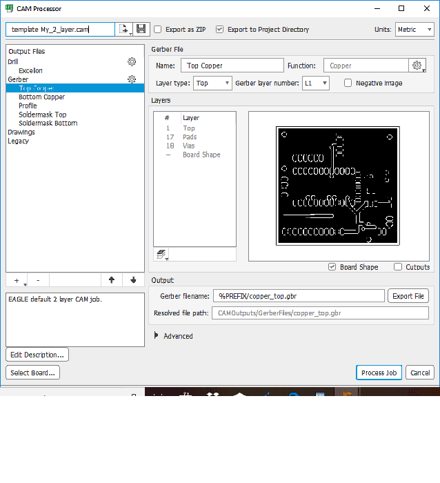
I like to use fill polygons to create a Ground plane on bottom and V+ on the top, thus I do not print the board image(s) directly but use Eagle's CAM output. I have not been using solder paste stencils since I hand-solder the few SMD components I use to my boards.
To facilitate the creation of the CAM images I created a custom template for single and dual sided CAM output containing the output files I need . I always add the board shape to the copper Gerbers but not to the masks.
I usually put the Gerber files into the Project folder when processing the job so they may be accessed if needed at a later date.
Converting CAM Images
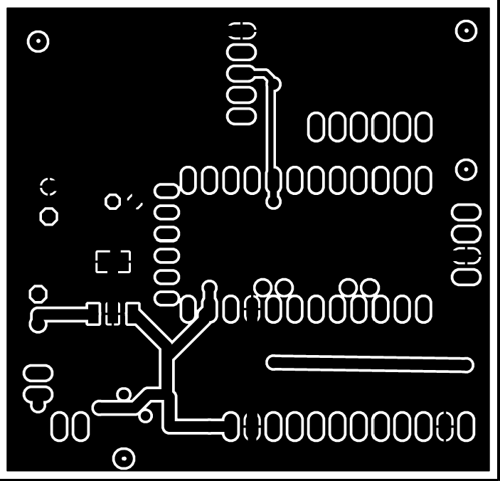
Creating the output using Eagle's CAM processor introduces several impediments to creation of the copper and solder masks.
- You need to convert the Gerber files into printable images.
- The Cam processor removes the component and via hole indicators.
The first step is to convert the Gerber files into some sort of image file which I can then edit and print. I use a utility named Gerber2PDF Gerber2PDF link.
The downloaded .exe is placed in the Eagle CAM directory. I then transfer the Gerber files I wish to convert from the Project directory to the CAM directory before running Gerber2PDF from the Windows command line.
See the Gerber2pdf documentation for the syntax to select and convert specific files.
I have included the text file I use to run the gerber2pdf process that you should download.
Feel free to edit this file to suit your needs. Cut the commands and paste them into the DOS command line utility to convert the Gerbers.
Once I have individual PDFs one for each copper and solder mask I need, I address the issue of the missing holes in board's components, vias and registration holes. I use PhotoShop to import the PDFs and edit the copper files to add the needed holes as small filled white circles.
Downloads
Editing Images
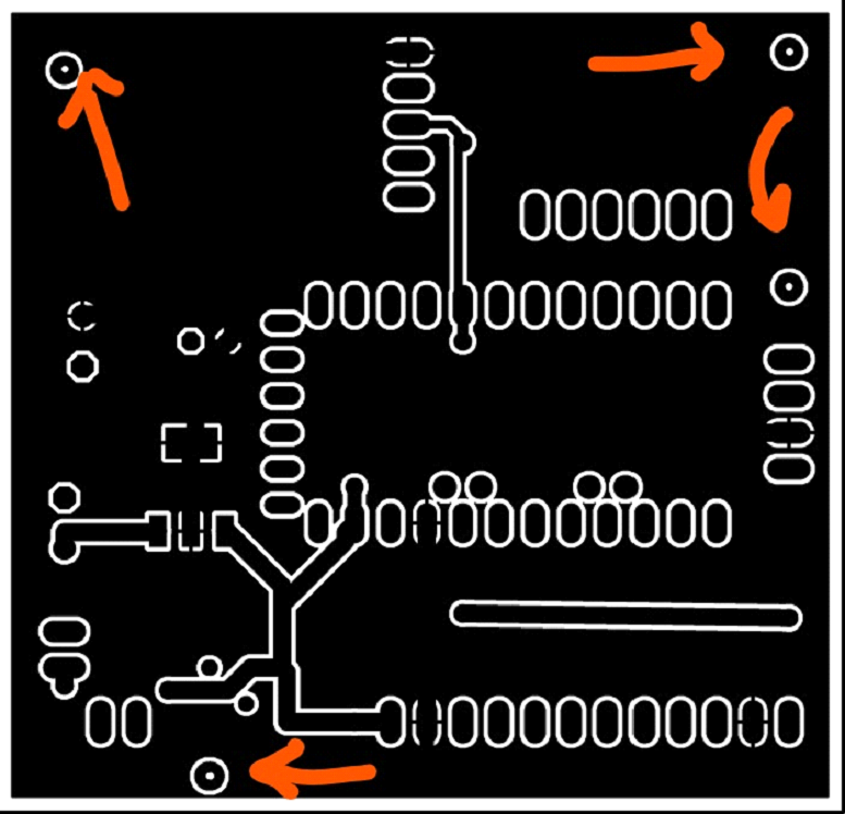
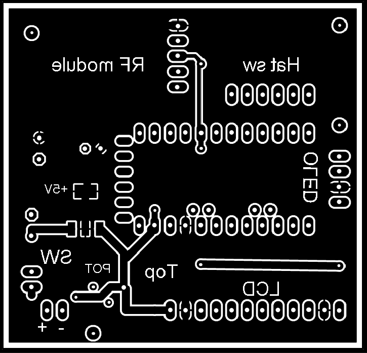
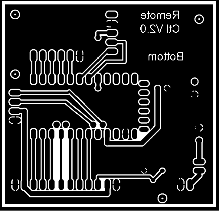
I use PhotoShop to import the PDFs and edit the copper files to add the needed holes as small filled white circles. You can use your own graphic conversion and editing software following the directions below.
Edit the PDFs to add registration hole marks (see Arrows) to both sides of 2- sided boards. Keep the registration holes extra small to make registration more exact but large enough to see when you print the copper images. I only add the component holes to the top since I will be drilling mainly from this side. Note the top copper image must be flipped horizontal (mirror) at this point so the pads will match after it is etched. You may also add printed text at this point. Be sure that any text you add appeared mirroredon both top and bottom copper so they will transfer to your board correctly(see above examples).
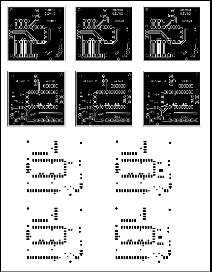
Copy and paste each copper and mask image into a blank, full page master sheet (at the same resolution as the PDFs) this will be printed on a your laser printer. You may also wish to add board identification text to the master sheet.
Putting multiple copies of the copper images on the master sheet will conserve paper and allow for mistakes in the toner transfer process. Do the same for the solder mask files adding at least 2 copies of each mask, they will be combined later.
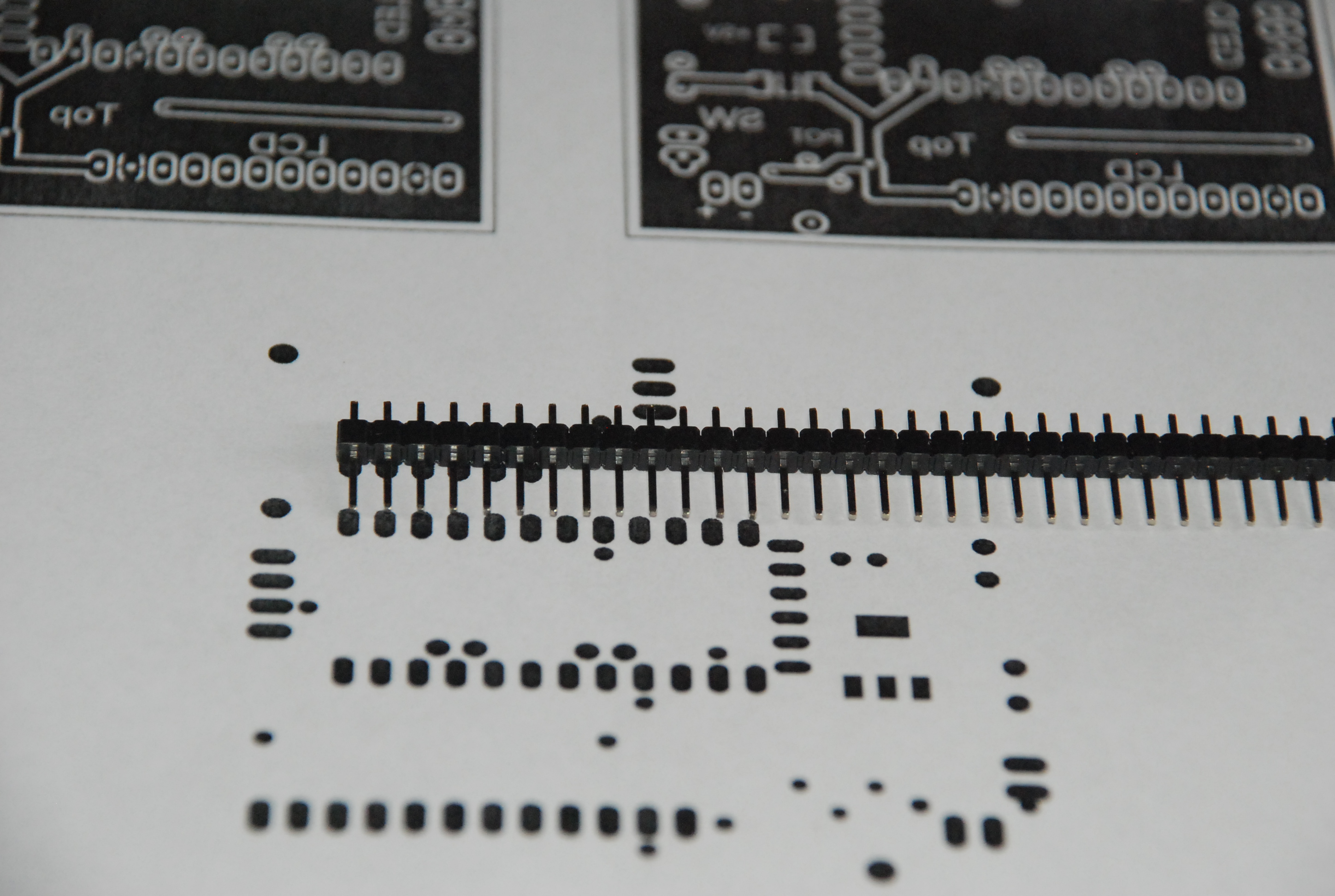
Print the Master Sheet
The printed Master Sheet copper images will be transferred to the prepared PCBs using toner heat transfer. I use Premium Color Laser Gloss Paper from Staples (#633215) for the transfer process. It is reliable, low cost and clearly visible (not like magazine pages). It accepts the Laser toner with little or no errors, transfers the toner to the copper quickly and releases cleanly with just a few minutes of soaking in warm water. If solder masks are to be generated at least two copies of each masks are printed on Laser Printer Transparency Film (C-Line no60837) .
Before you print on the gloss paper or transparencies print a copy of the images on plain paper. This copy will be used for board sizing and 2 sided copper alignment. It is a good idea to check for correct distances between pads for SMD and other components (see above photo). Do this for both the copper and mask images. I have made mistakes in the copy and paste process more than once and, after etching, masking and drilling the PCB, could not populate the finished boards
Prepare Copper Coated Board
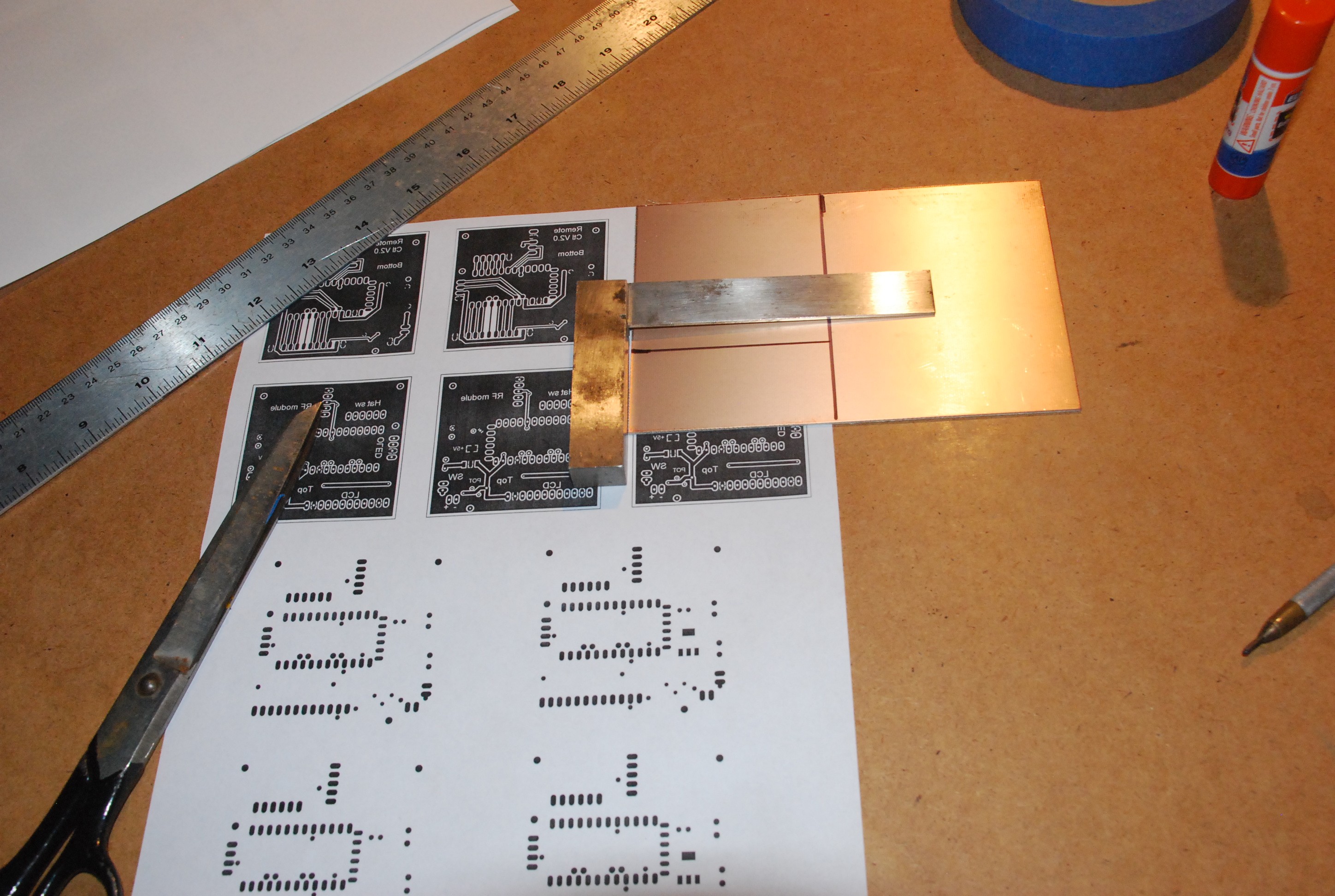
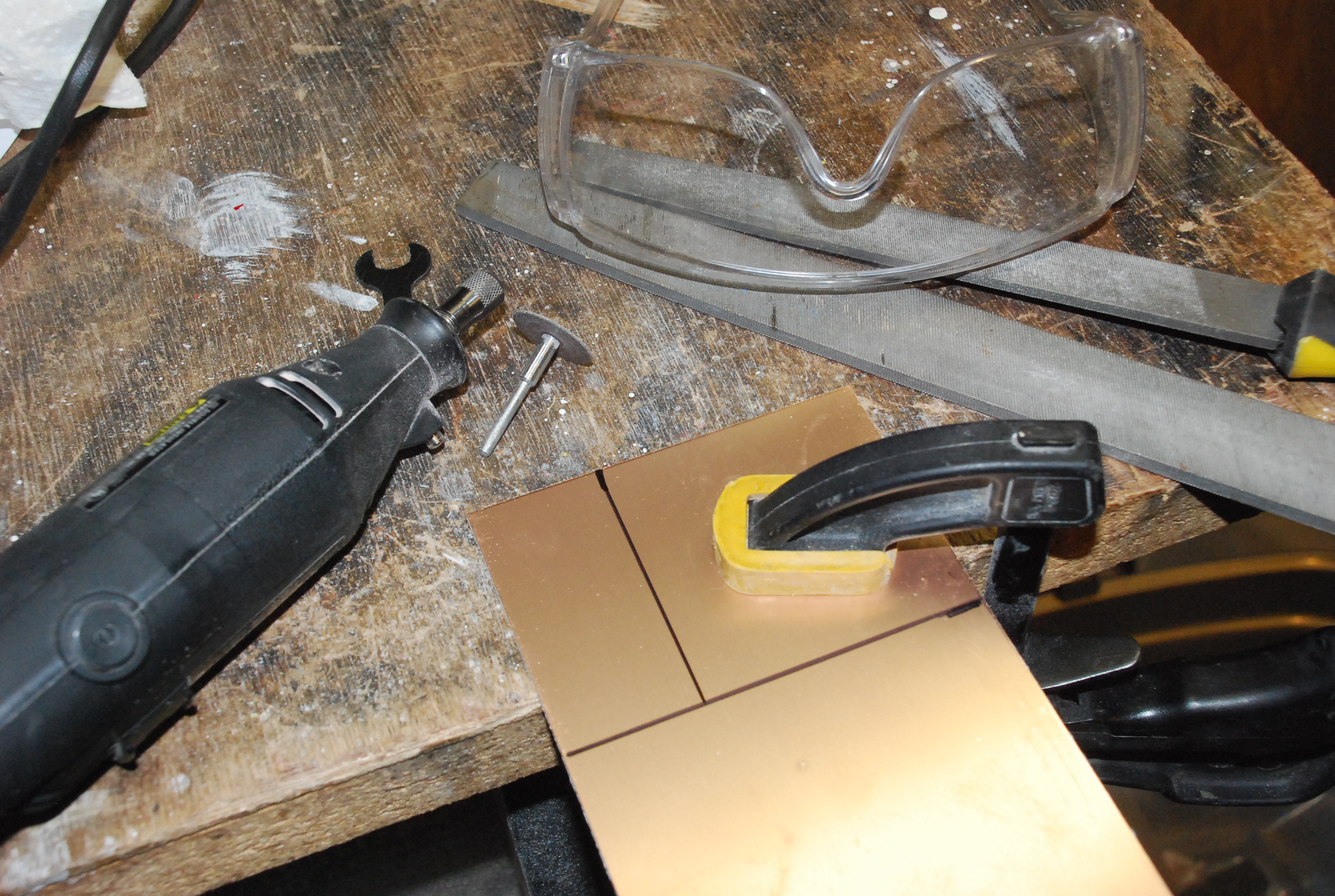
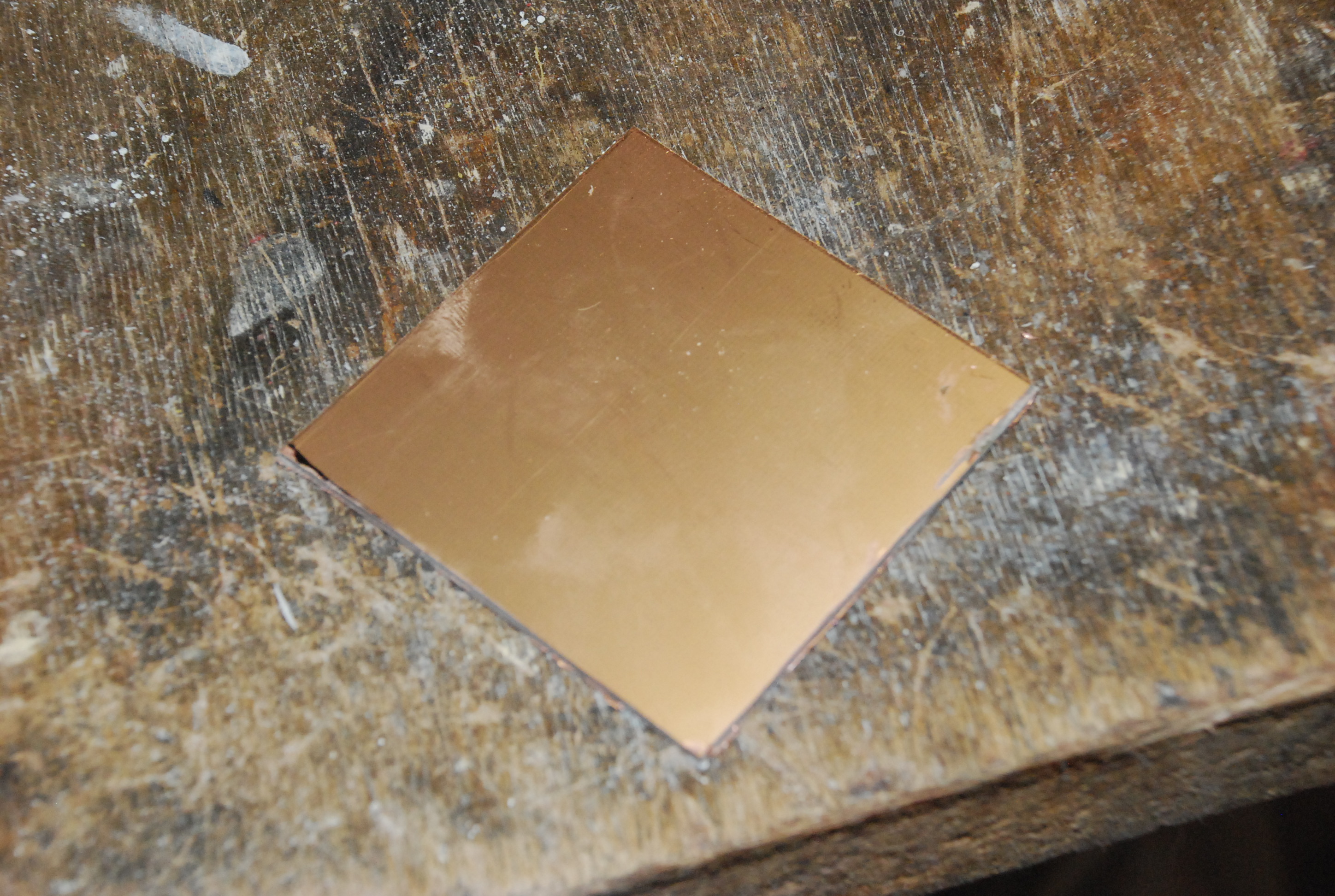
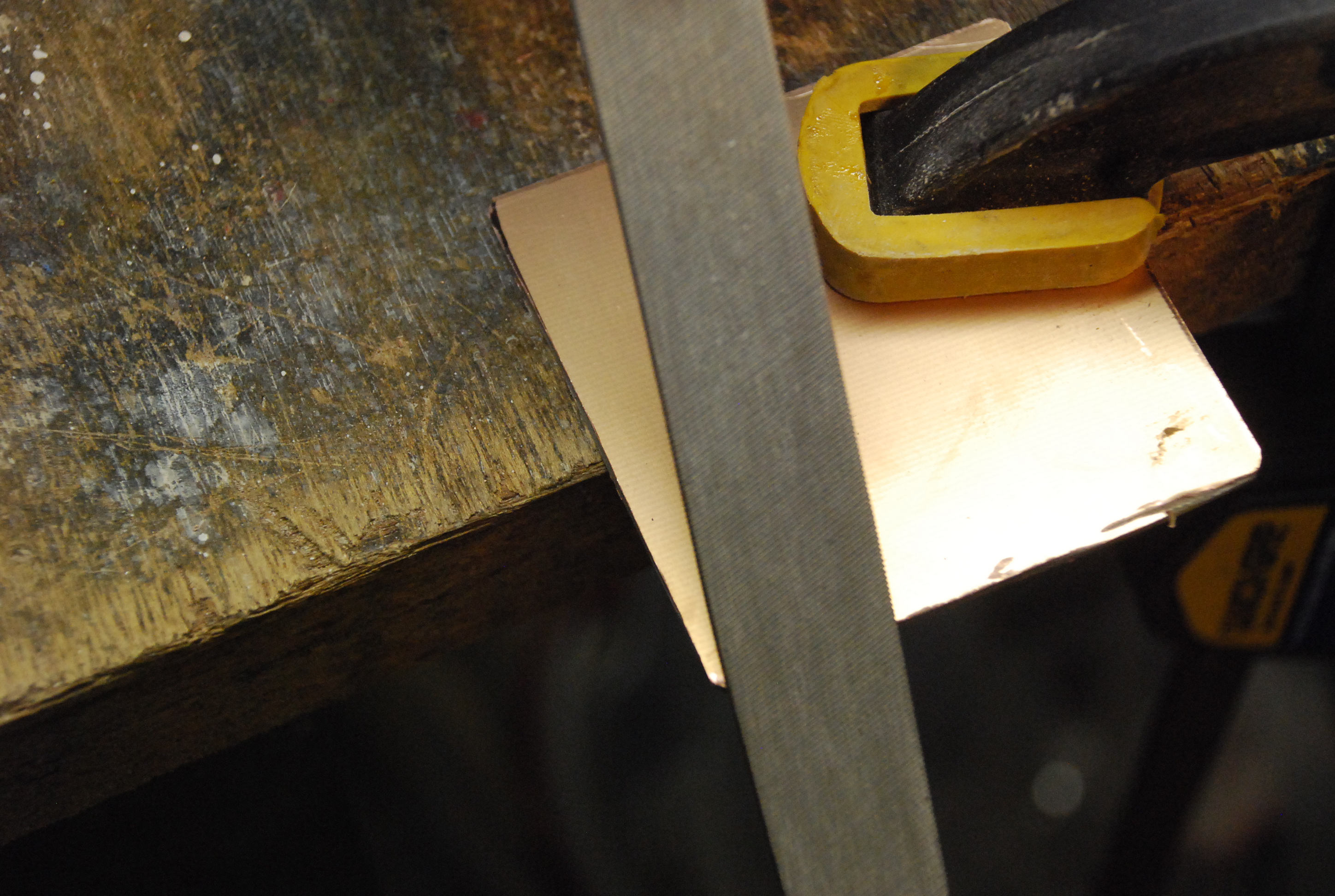
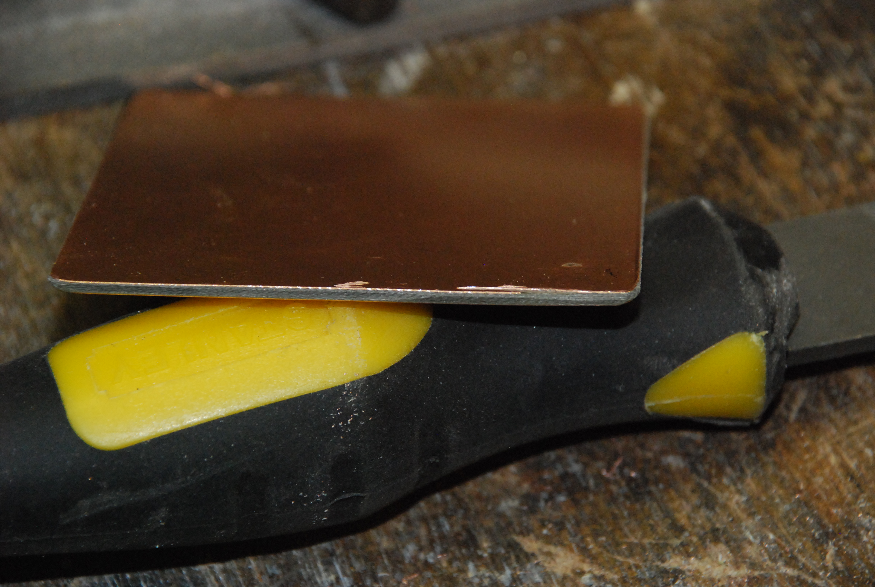
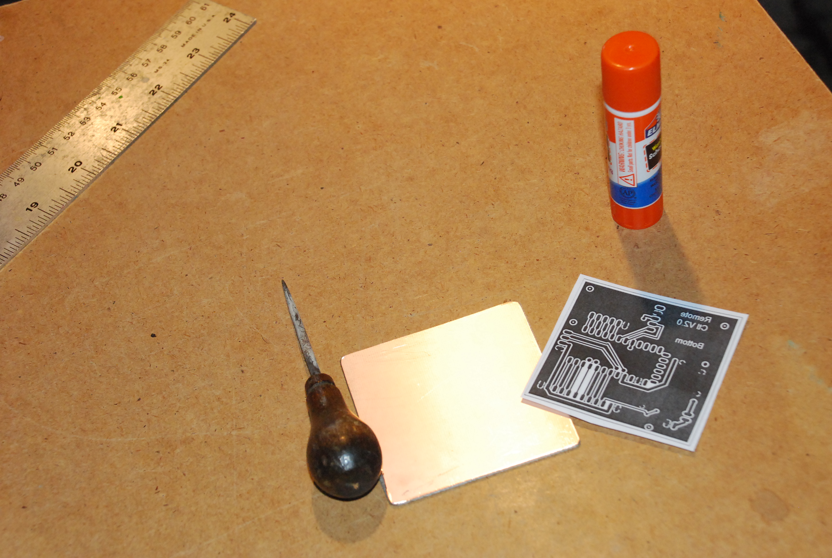
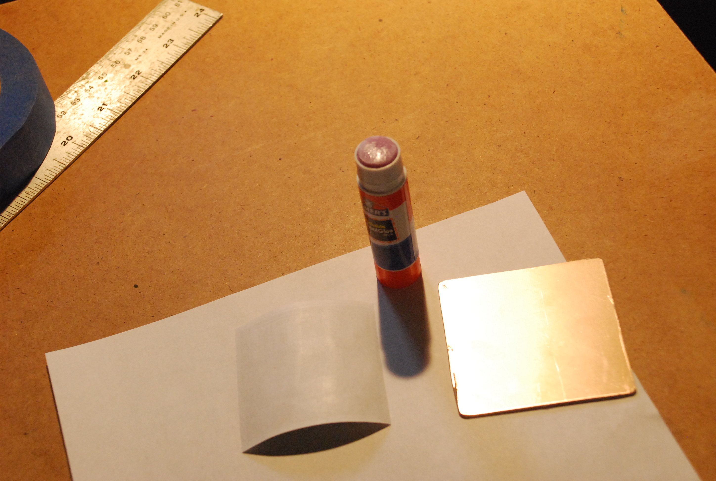
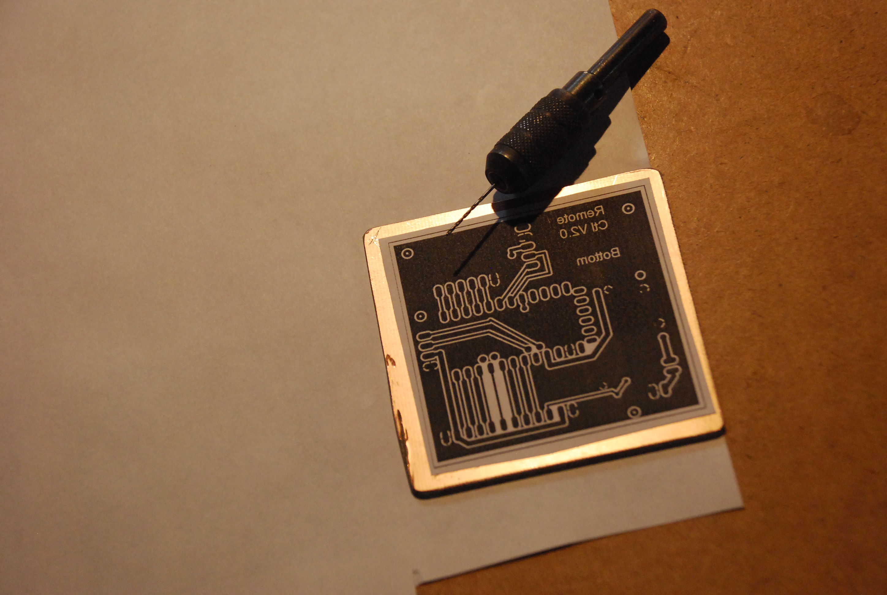
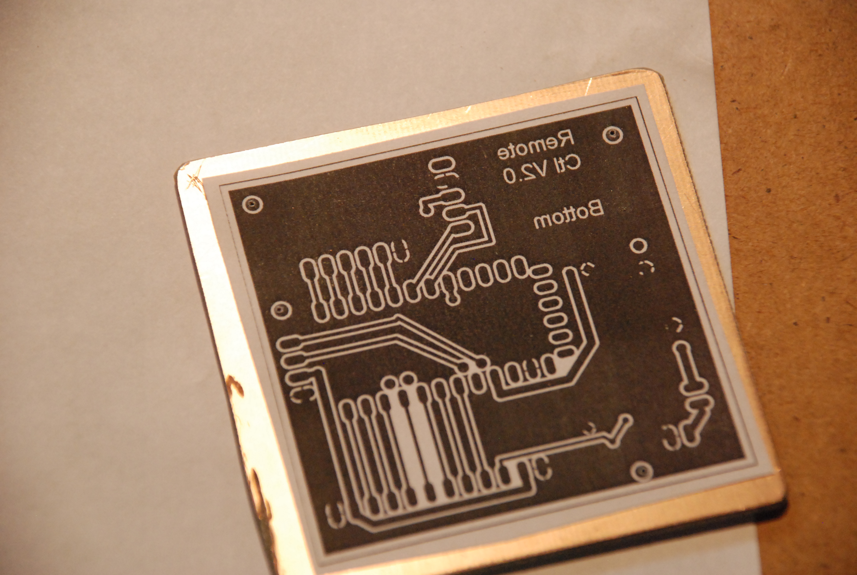
The copper boards (single or dual sided) are cut to rough shape (~ half inch all arround) using an image from the plain paper printout as a guide (I use a Dremel tool with a cut-off wheel).
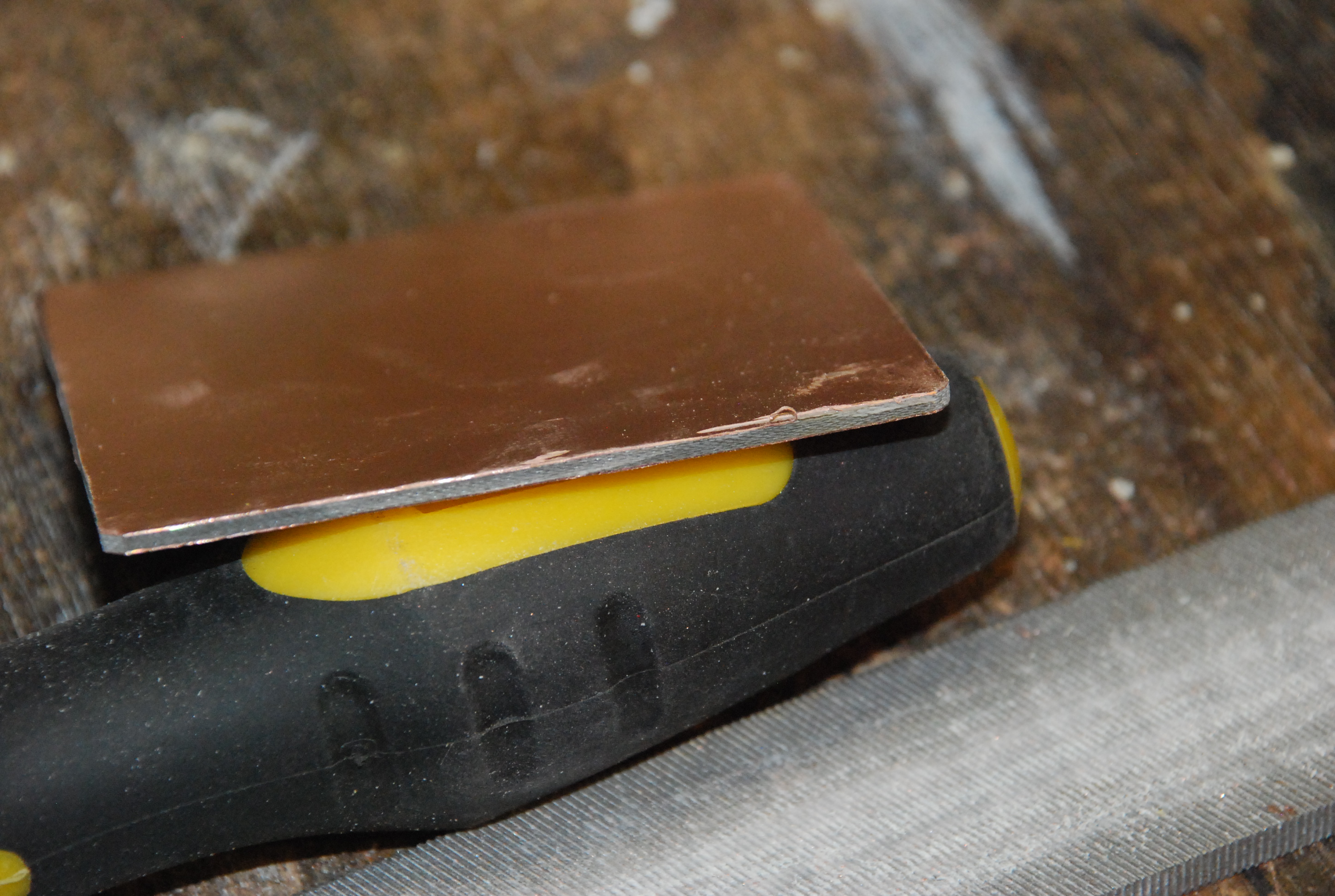
The edges are filed smooth to flatten them and the corners rounded. I then file the top and bottom edges at a 45 degree angle to remove any burrs or sharpness (check with your finger after filing).
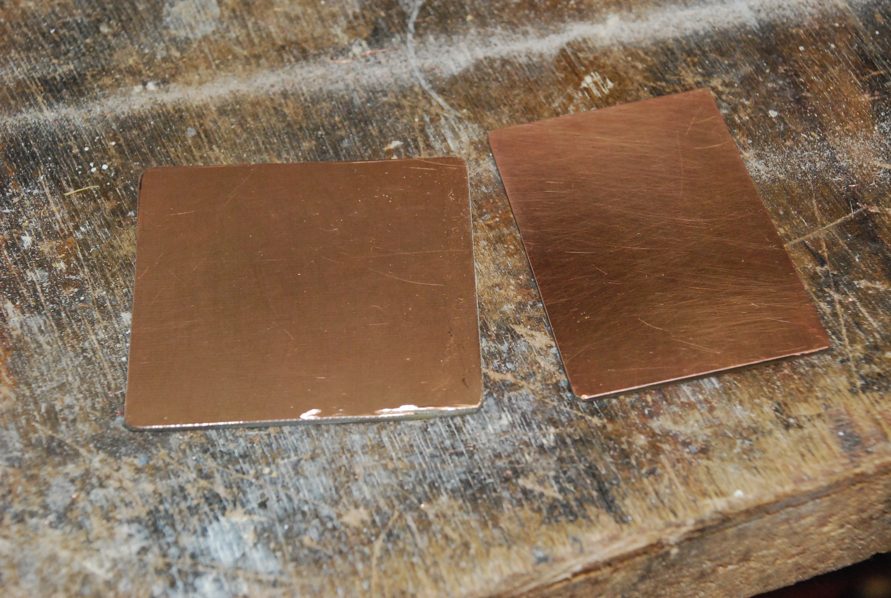
The next step is to clean the boards to remove any oils or grease. Detergent and warm water will do the trick. Finally to remove oxidation and create a surface that will accept the transfer and be easy to solder, I sprinkle the copper with a little "Bar Keepers Friend" compound and scrub gently with a damp sponge, then rinse before drying with a paper towel.
If the boards are 2-sided, the images will need to be registered exactly. I found the best way for me is to temperarely glue a plain paper copy of the bottom copper image to one side of the board (paradoxically this will be the top) and carefully drill the centers of the registration vias with a #70 drill. A drill press with a drill vice to hold the bit works well.
Register Copper Images
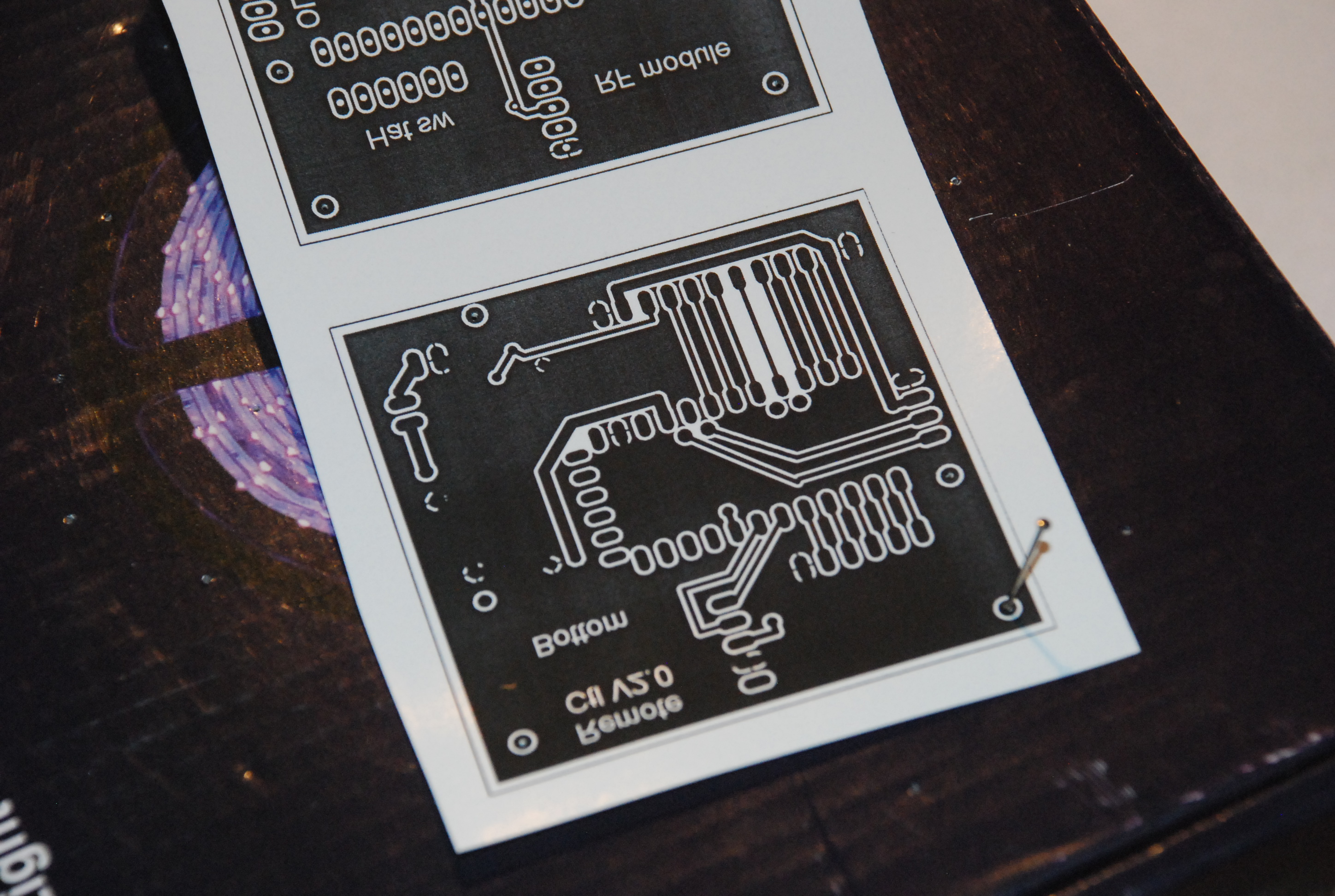
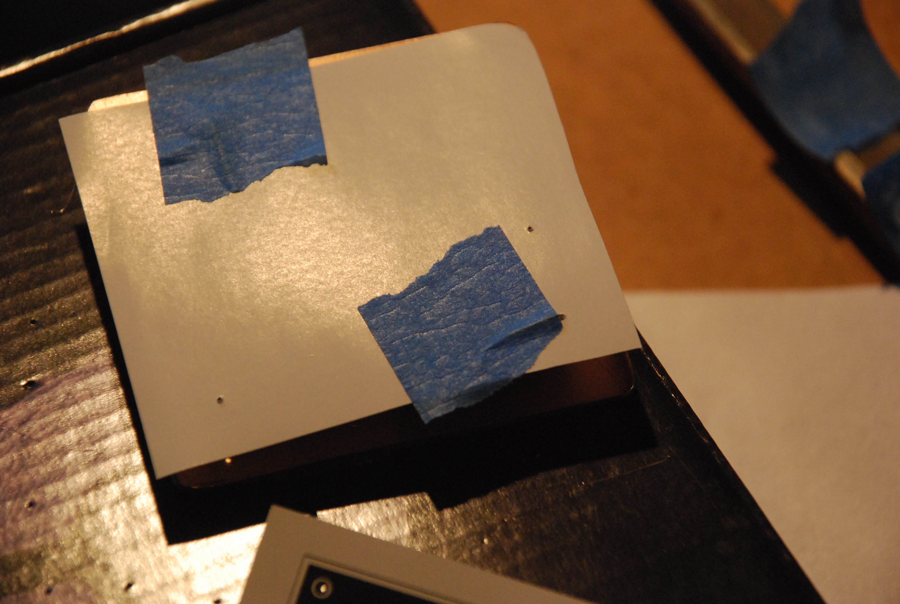
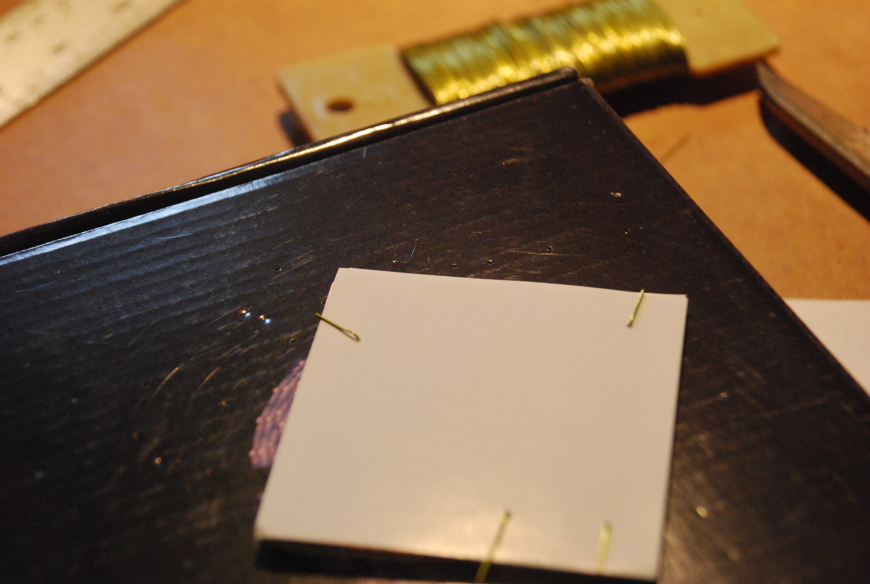
For single sided boards the process is fairly simple. Just cut out a copy of the copper image from the glossy paper and gently tape it to the board image side down using painters tape (blue tape). I then place the board on a piece of plywood covered with 2 layers of paper toweling and cover the board with another two layers.
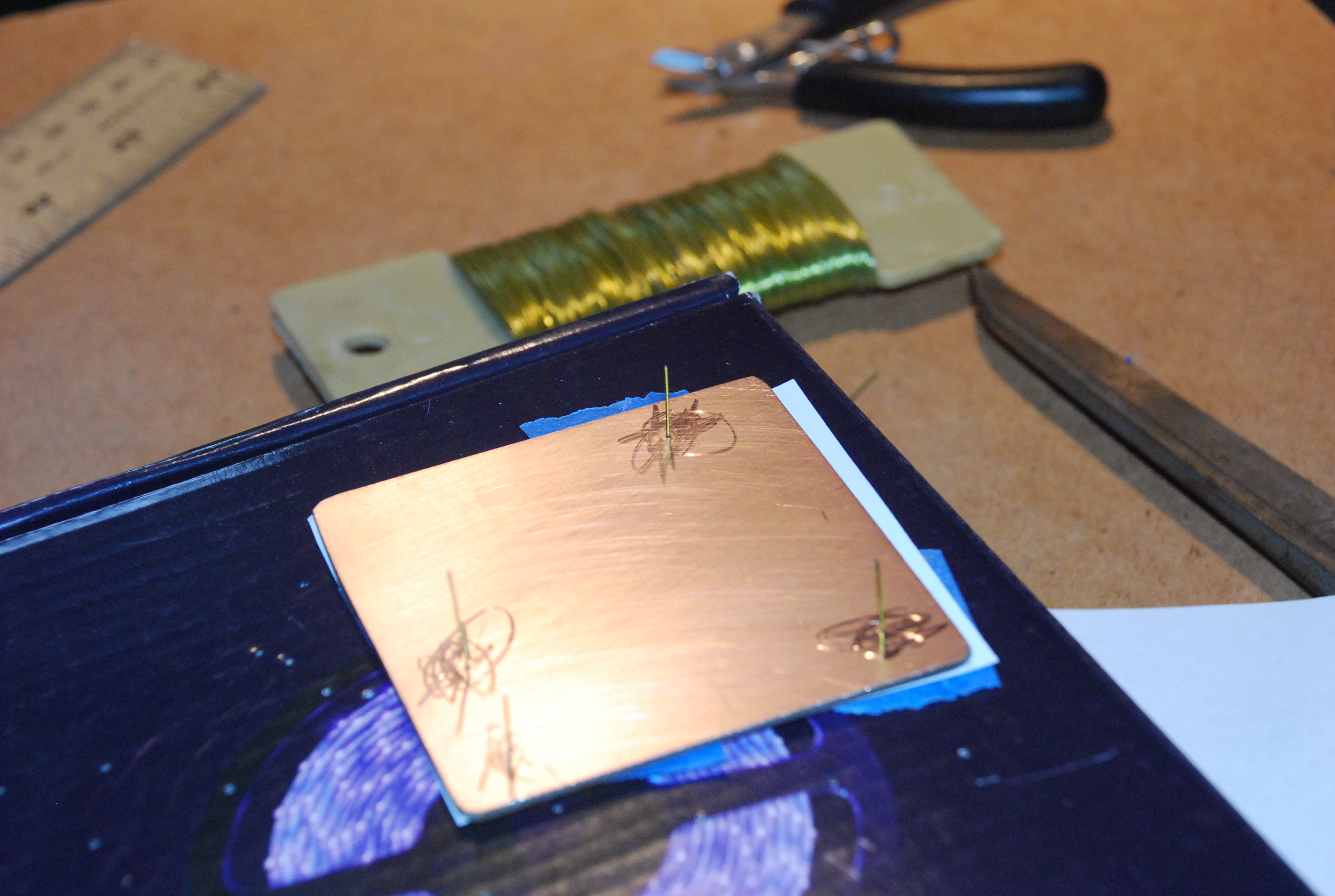
For two sided boards the process is more complicated. I first clear the registration holes in the board with a straight pin. The next step is to cut out one copper top and one bottom image from the glossy paper and exactly pierce the center of all the registration holes with a straight pin.
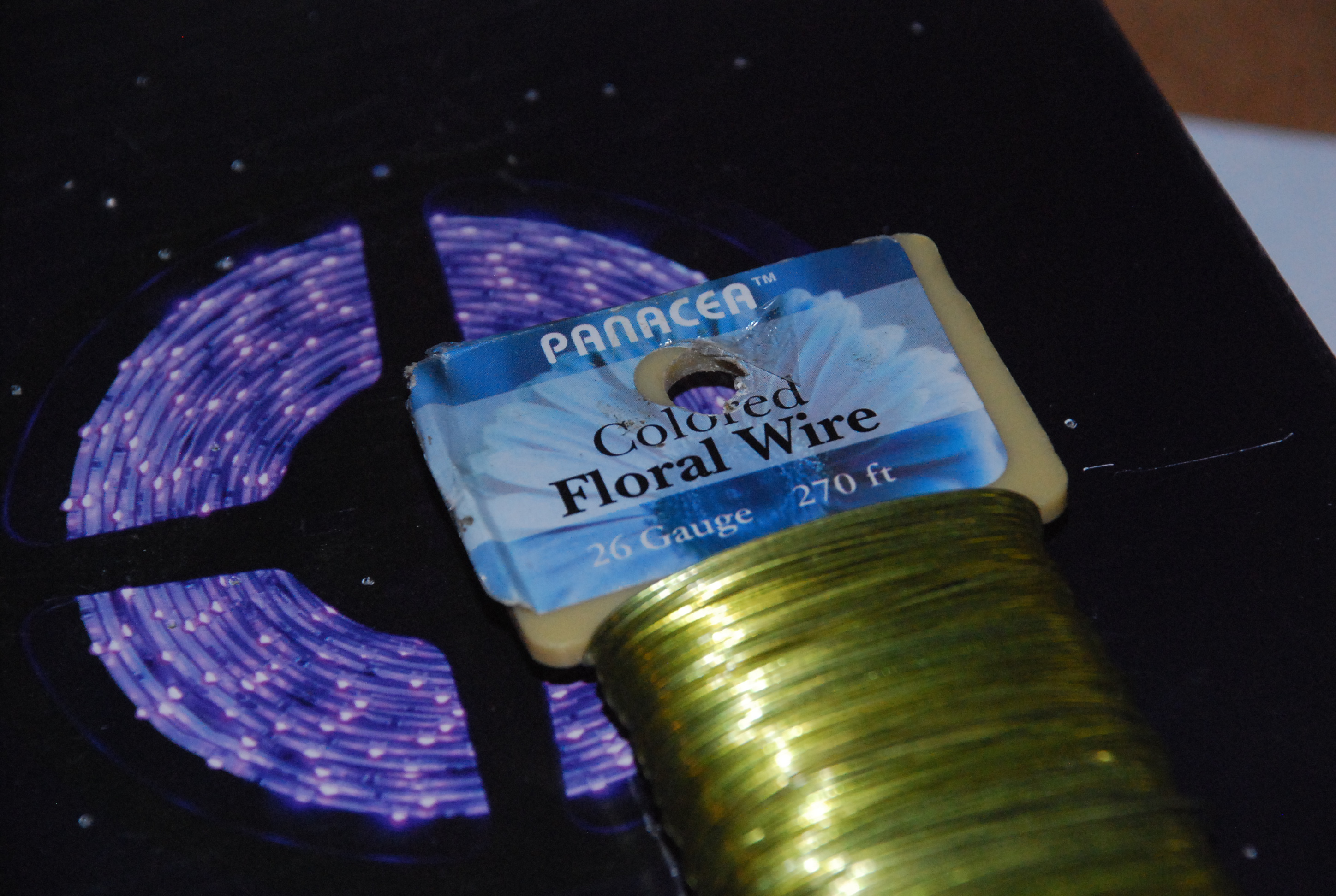
Next I cut pieces of thin ( ~ 26 gage) florist or craft wire small enough to pass through the registration holes (about 3/4 inch in length). I pass this wire first through the back of one of the registration holes in the top paper, then through the board. At this point I bend the wire and use a small piece of painters tape to prevent the wire from dropping through when I flip the board over. Finally push it through the front of the bottom paper holes so that the images are facing the copper.
Each wire is then bent to hold the papers and board together. When all the holes are completed, follow the procedure for the single sided board above.
Toner Transfer
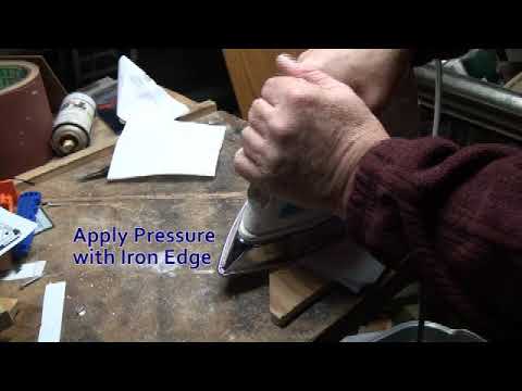
Now that the board is ready for the toner transfer. This video of the transfer process may make the following instructions clearer.
I apply a dry clothes Iron set to just under the highest temperature to tack down the paper to the board using the pointed tip of the iron. Be careful to place the tip between the wires on two-sided boards and tack down both sides so that the paper does not separate from the board when handled. Warning the board gets burning hot. On two sided boards I snip the wires flush on one side then pull the other ends through the paper and board before the next step.
Remove any tape before applying the iron with pressure on each side for about 1 minute no movement unless the board is to big for full iron coverage. This will heat soak the board and tack on the toner. To assure toner transfer I remove the paper towel on the top side and hold the edge of the iron at a 45 degree angle to the board then apply pressure while moving across the board . I do this on each side at least several times. At this point you should see a slight image of the toner on the back of the paper.
The next step is to soak the board and paper in water till the paper floats off. I usually gently rub the back of the paper to remove the clay coating to facilitate the process and gently peel the paper off after a few minutes, A light brushing under water with a soft bristle brush or your fingers will insure the clay coating of the glossy paper is removed from the copper before etching. The water will cloud-up with microscopic clay particles.
Dry, inspect and touch-up with a Sharpee Marker and knife if needed. If extensive repair is needed at this stage you might want to remove the toner and reapply before etching (be sure to clean the board again).
Etch Your Board
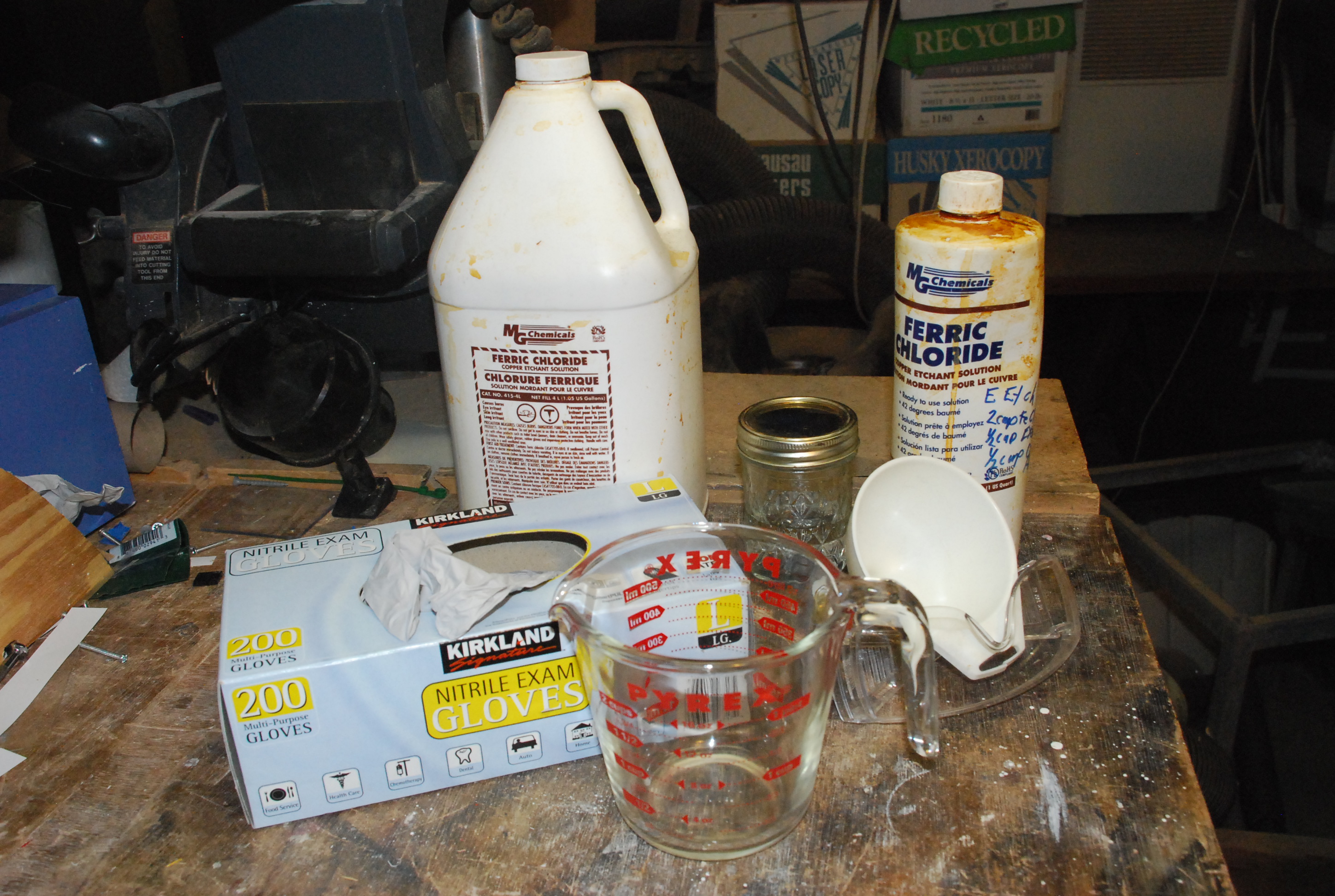
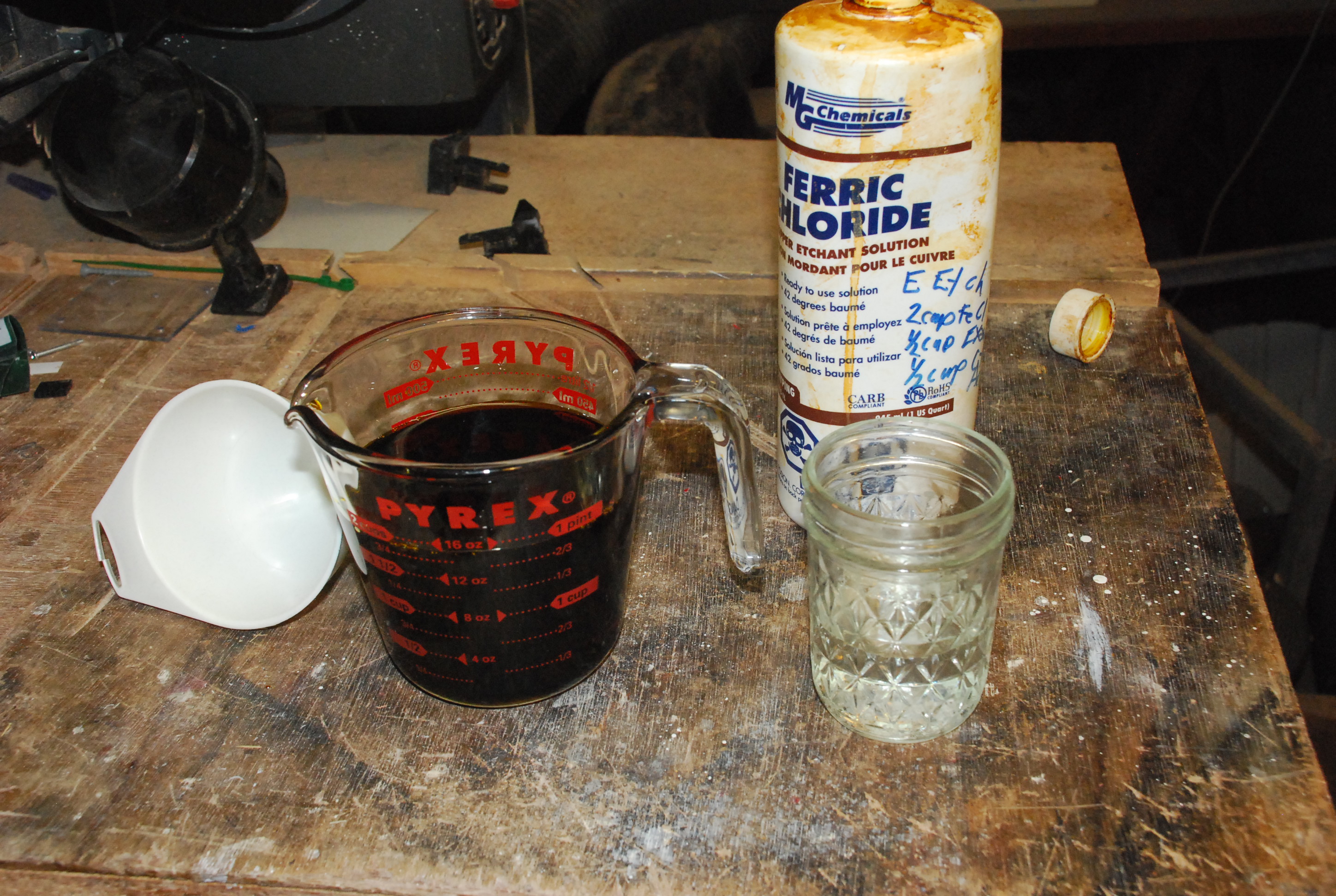
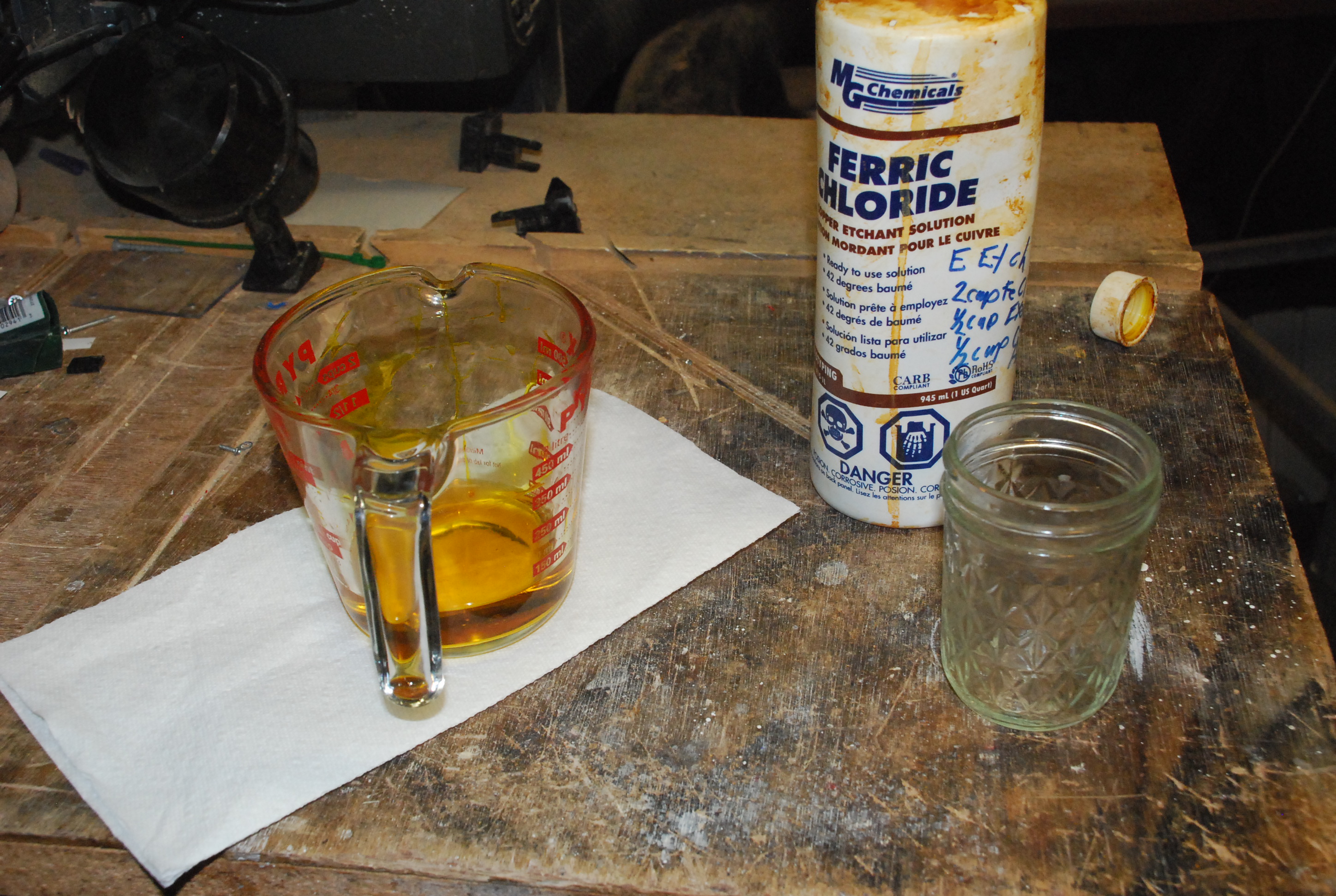
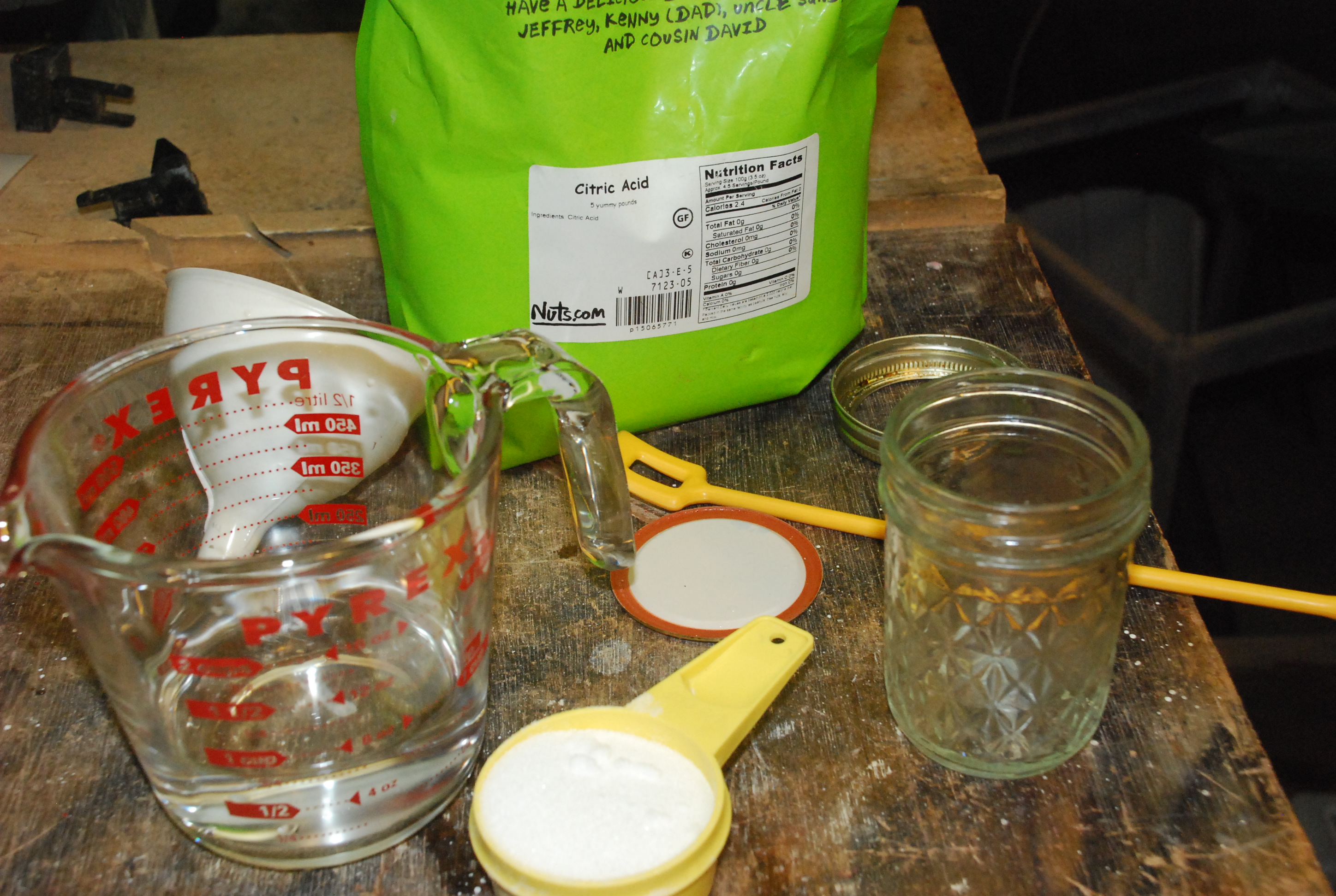
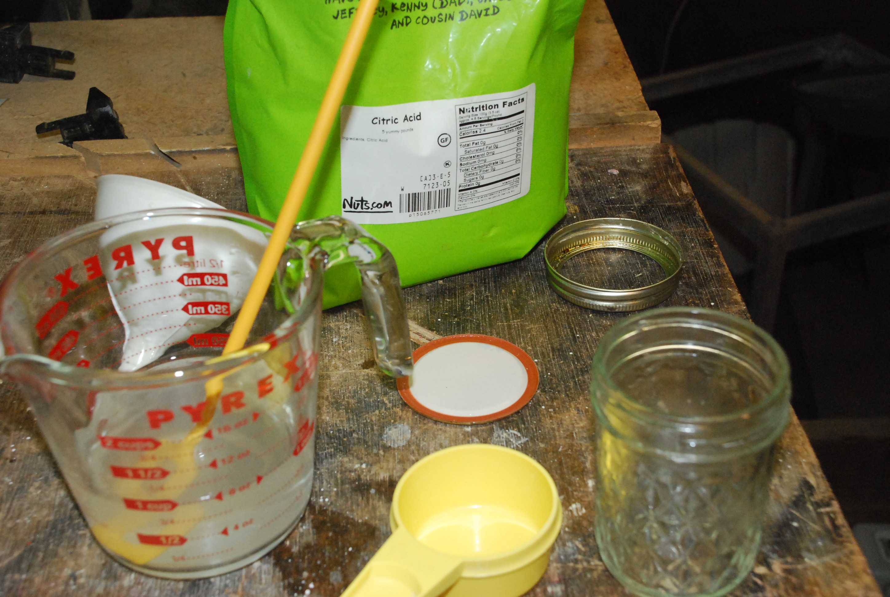
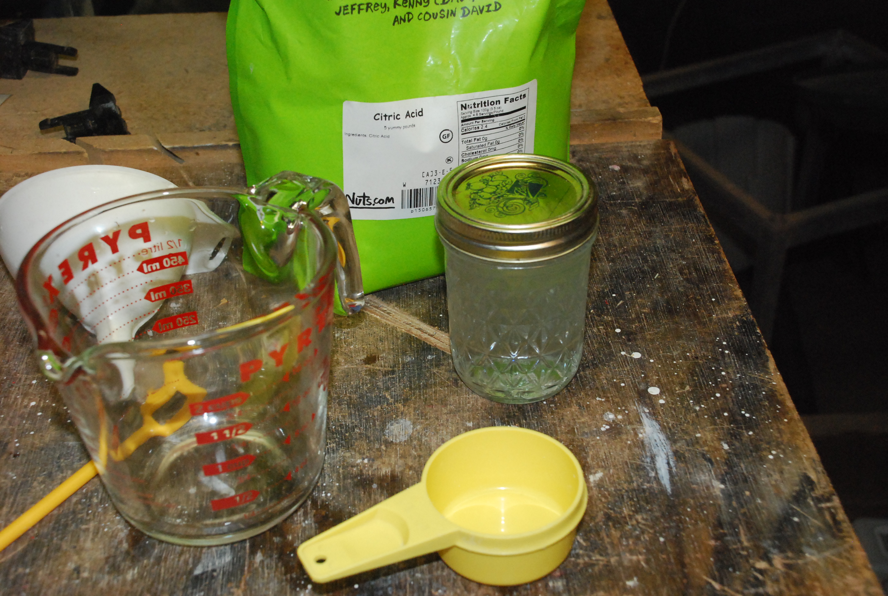
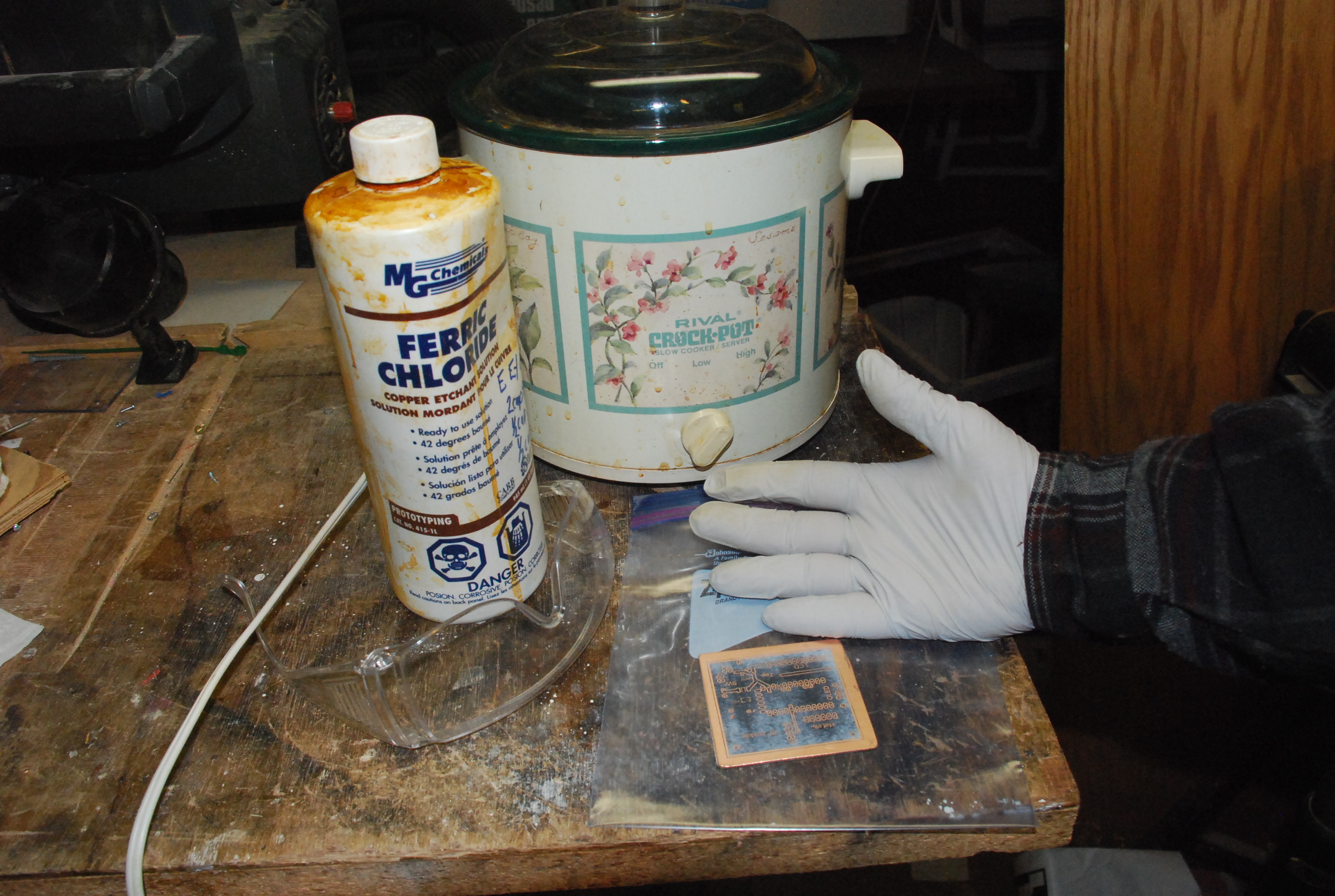
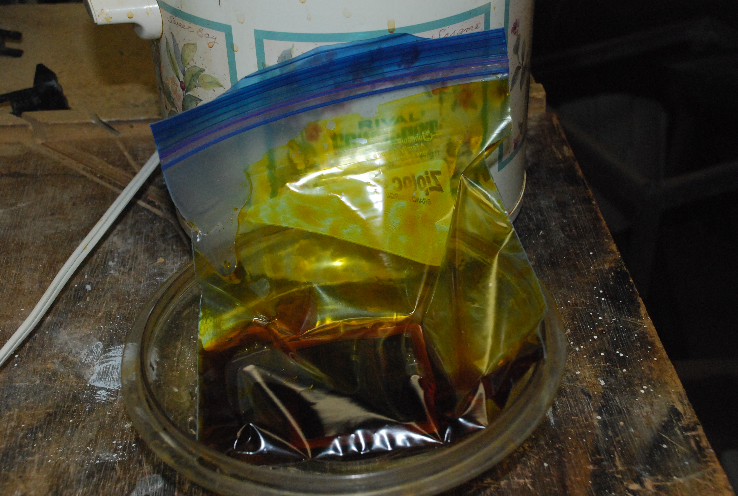
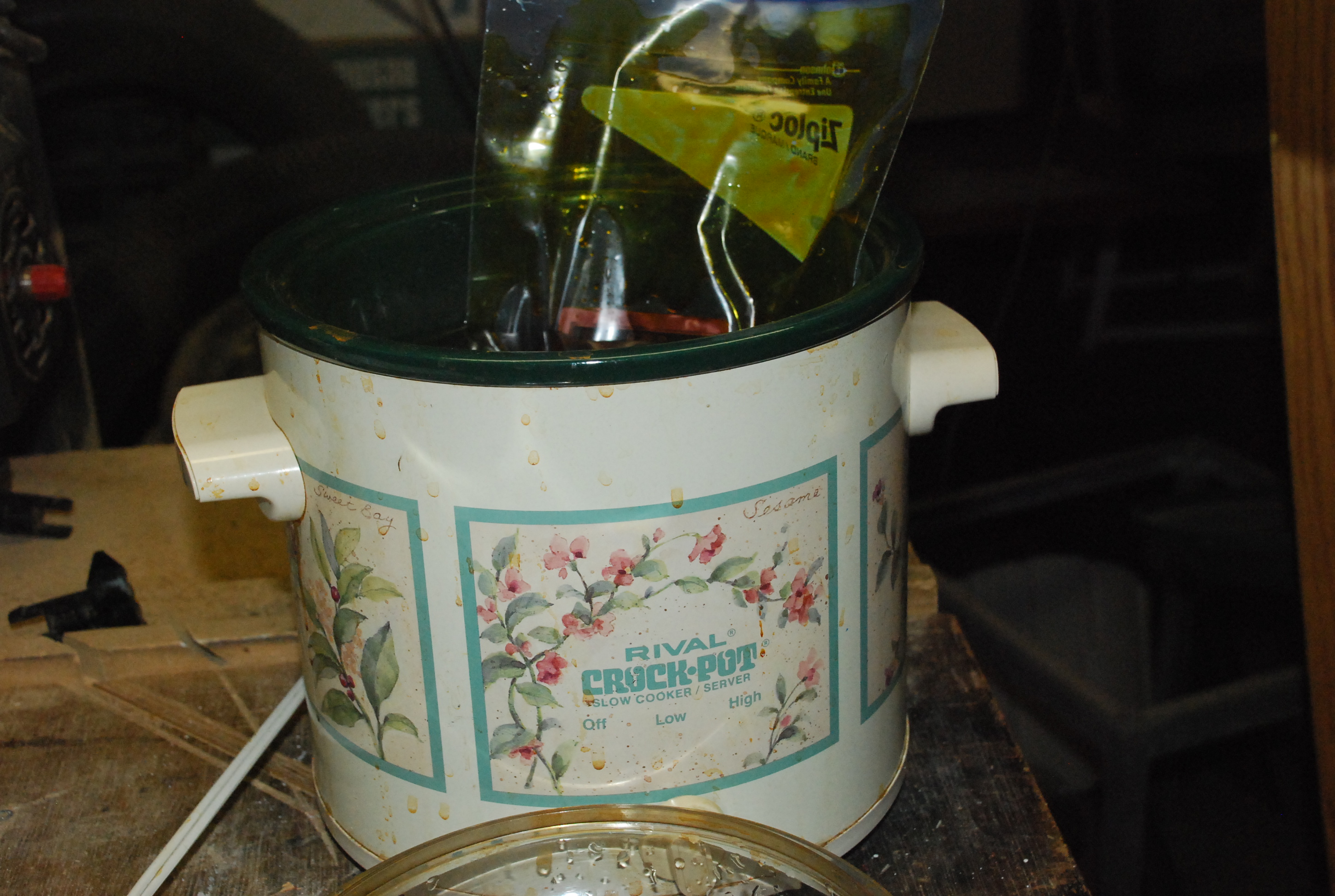
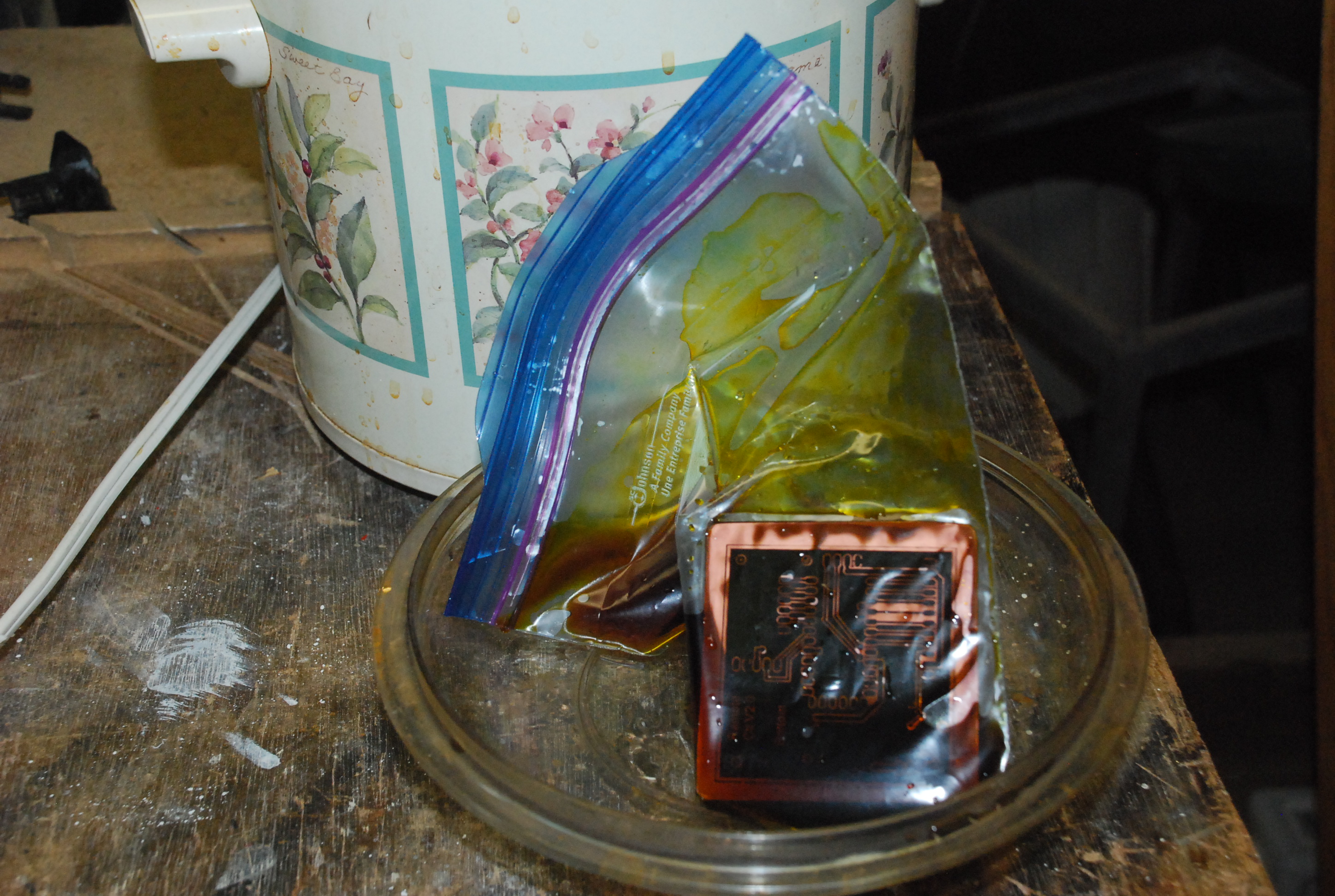
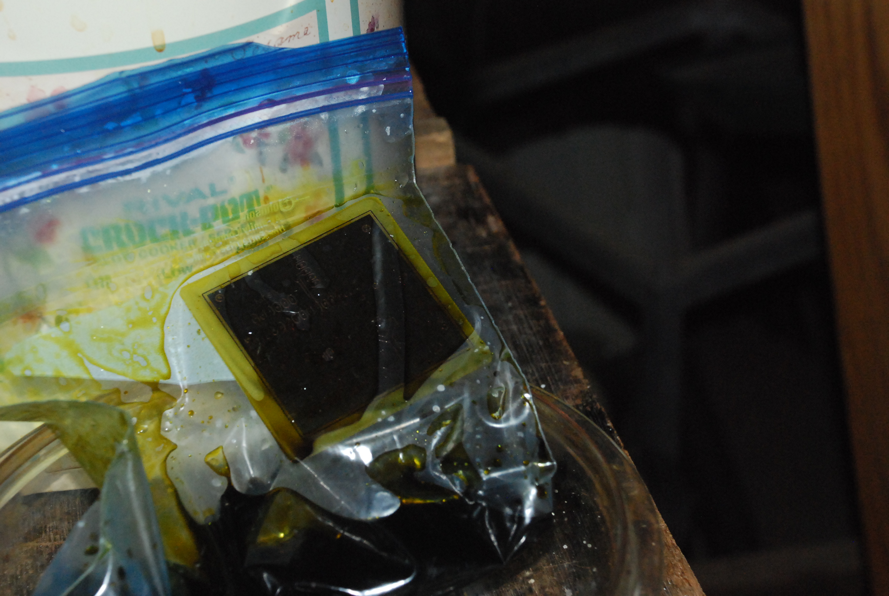
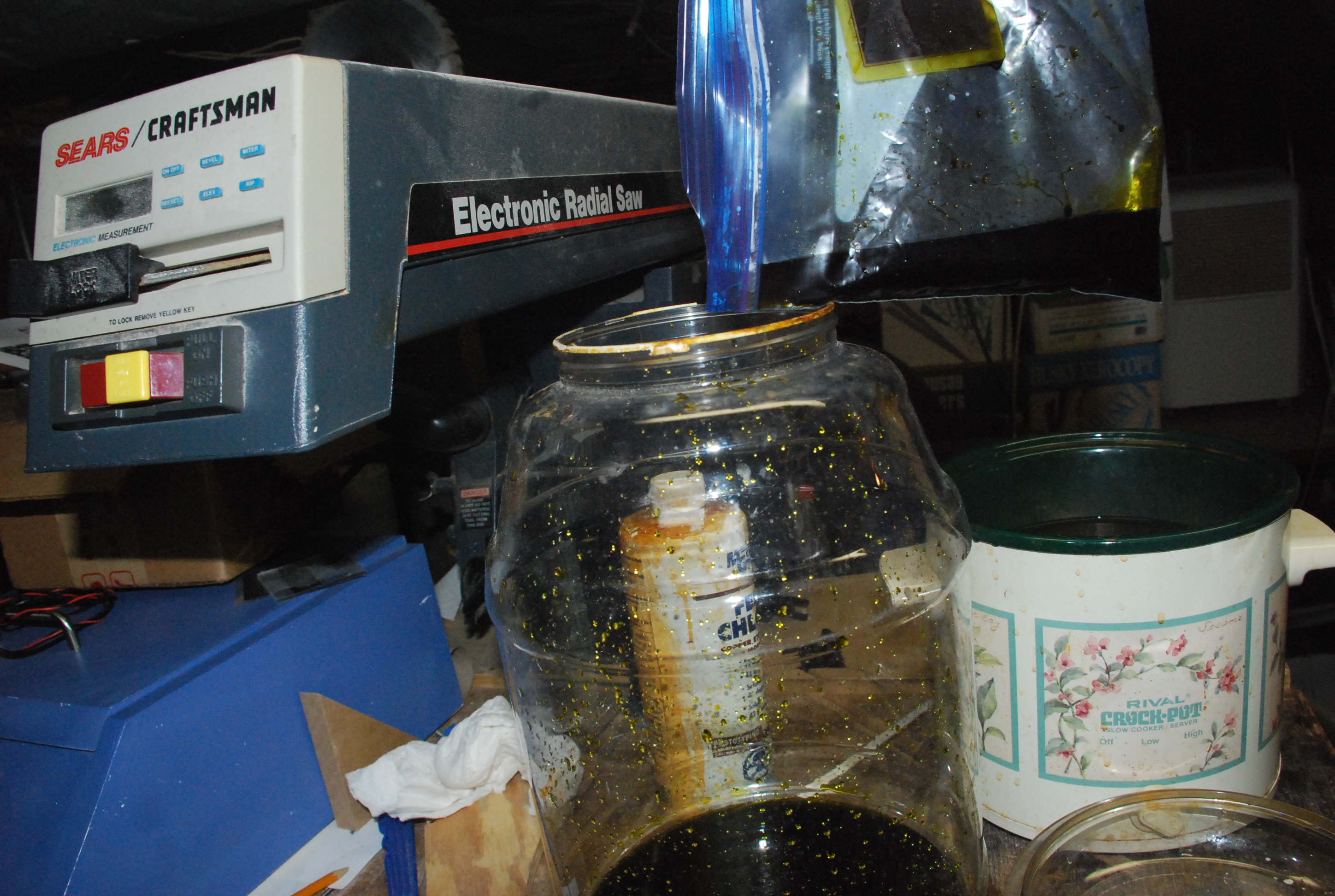
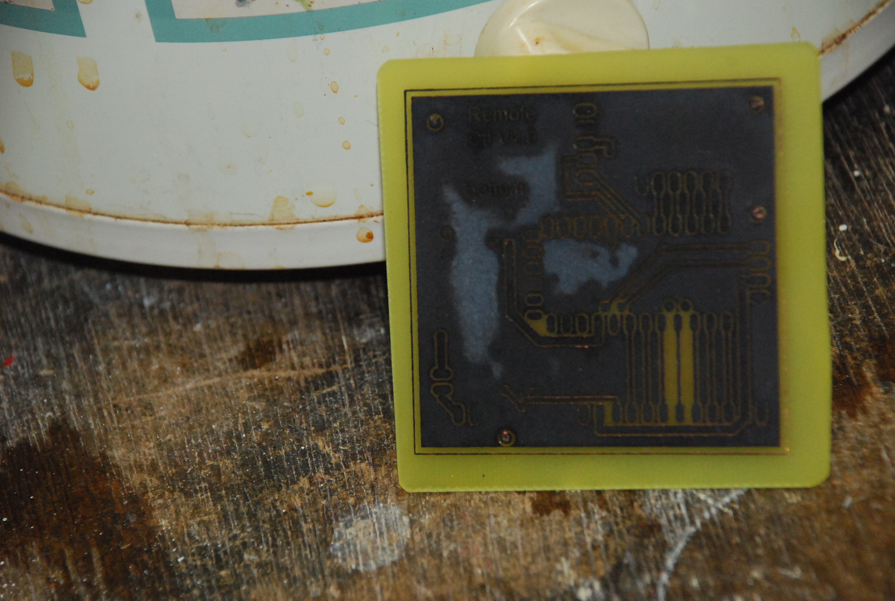
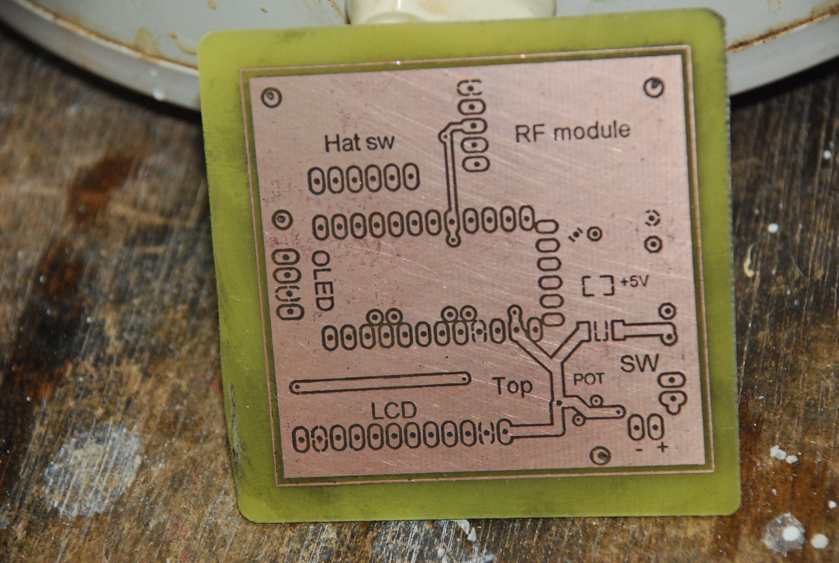
My etching process is perhaps the most unconventional. It requires a crock pot filled 1/2 way with water set on the high setting and heated( at least 1 Hr) until hot. The next unusual step is to etch the board inside a good quality freezer bag with a zip lock. Finally I use a Ferric Chloride based Edinburgh Etch which is prepared as follows: Obtain some dry Citric Acid (also know as Sour Salt often used as a food preservative} from an on-line (NUTS.com) or local source. Prepare a solution of Citric acid by dissolving 1/4 cup the powder in 3/4 cup of warm water,set aside to cool. To make the etchant add 1/2 cup of this solution to 2 cups of 40% ferric chloride solution. Add the acid to the chloride. This is the Edinburgh etch. The etching solution is twice as fast as plain Ferric Chloride etch and will not self clog or form the sludge.
WARNING: Do NOT use a Hydrogen Peroxide based etchant with this method. It generates Hydrogen gas that is explosively flammable and will burst the bag open.
Be sure to use gloves and clothing protection (a waterproof apron) before mixing or using the etchant. It will still stain and eat cloth and skin! Open the bag with the circuit board, I usually add water to the bag first to test for leaks then dump that water out. Add etchant sufficient to etch your circuit, do not overfill, you can always add more later but, it can be messy. You will find that you will use less etchant than with other methods and since it is discarded after use, the etchant is always fresh. Squeeze as much air as possible out of the bag without spillage then the securely seal it closed so it is air tight.
Turn off the crock pot. Now place the bag in the hot water till the board is submerged and flat. Check on the progress of the etching at least every 5 minutes till all the exposed copper is completely cleared (the clear bag allows inspection). There is no need for constant agitation since the Edinburgh Etch does not clog. When complete (no copper visible), remove the bag and carefully open it, discard the etchant in a waste container, do not pour it down the drain! I use a large plastic container with a wide mouth that I take to my community hazardous waste collection to discard.
Rinse the bag out with water, also discard into your waste container and remove the board before discarding the bag. Rinse the board under running water to clean before removing your protective gear.
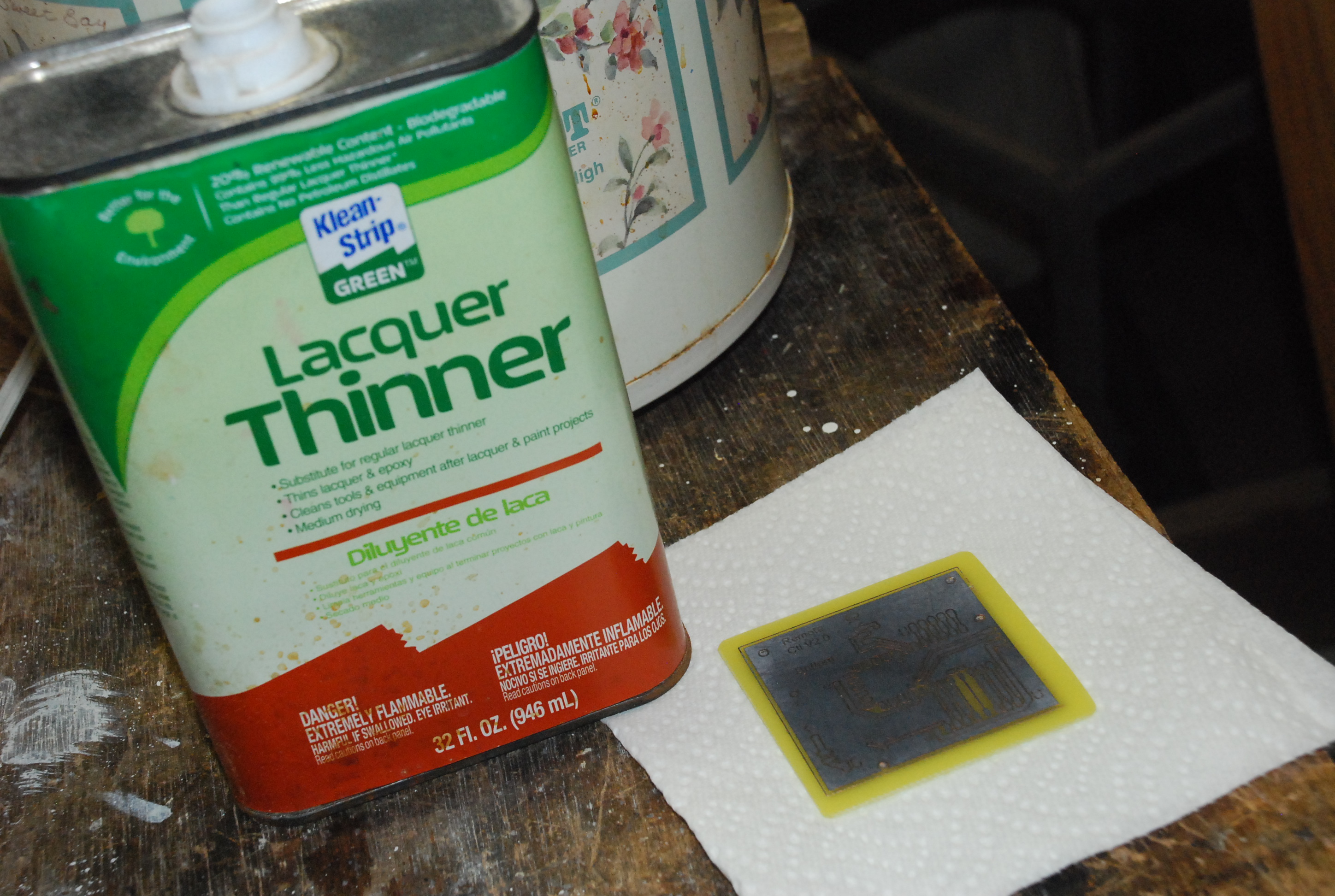
Removing the toner as usual by wiping with a paper towel dipped in acetone or lacquer thinner.
Apply Solder Mask
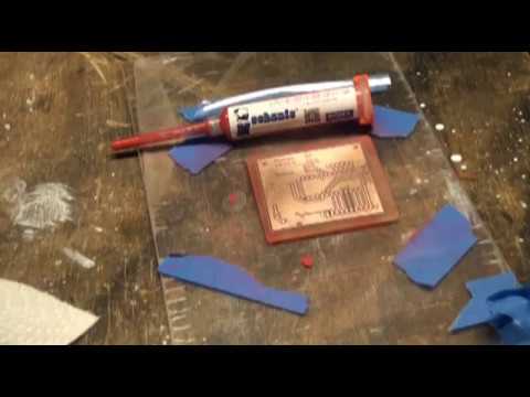
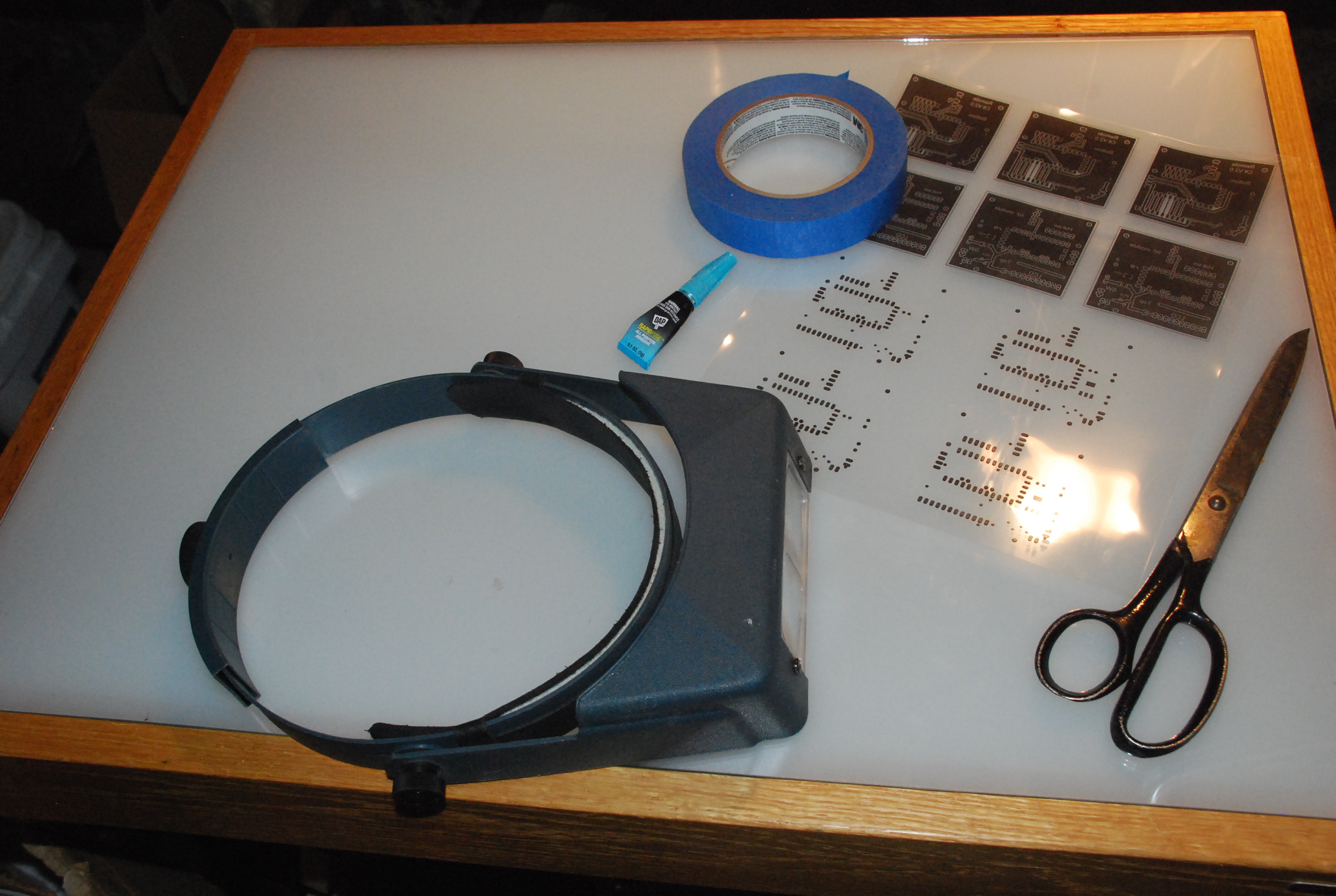
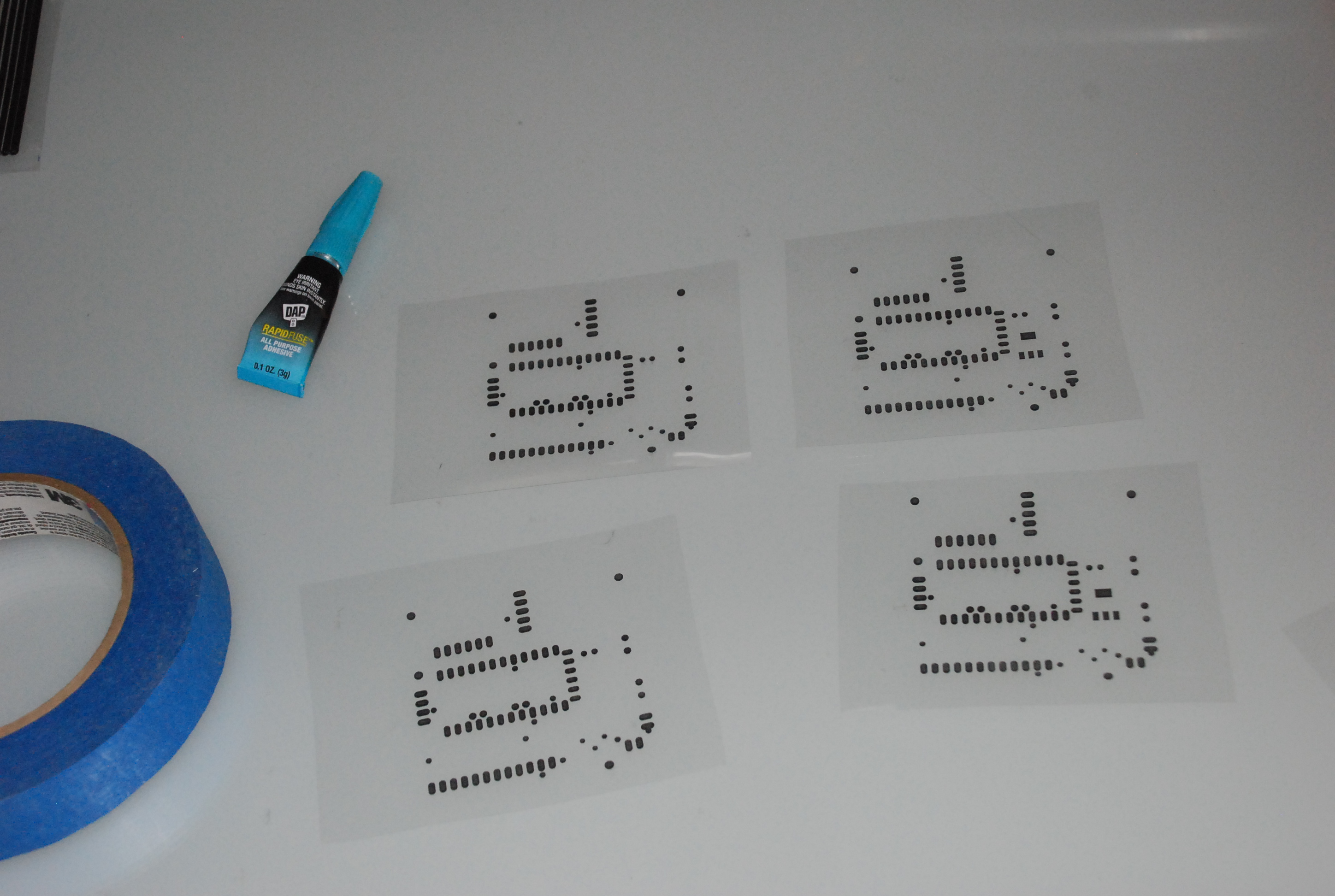
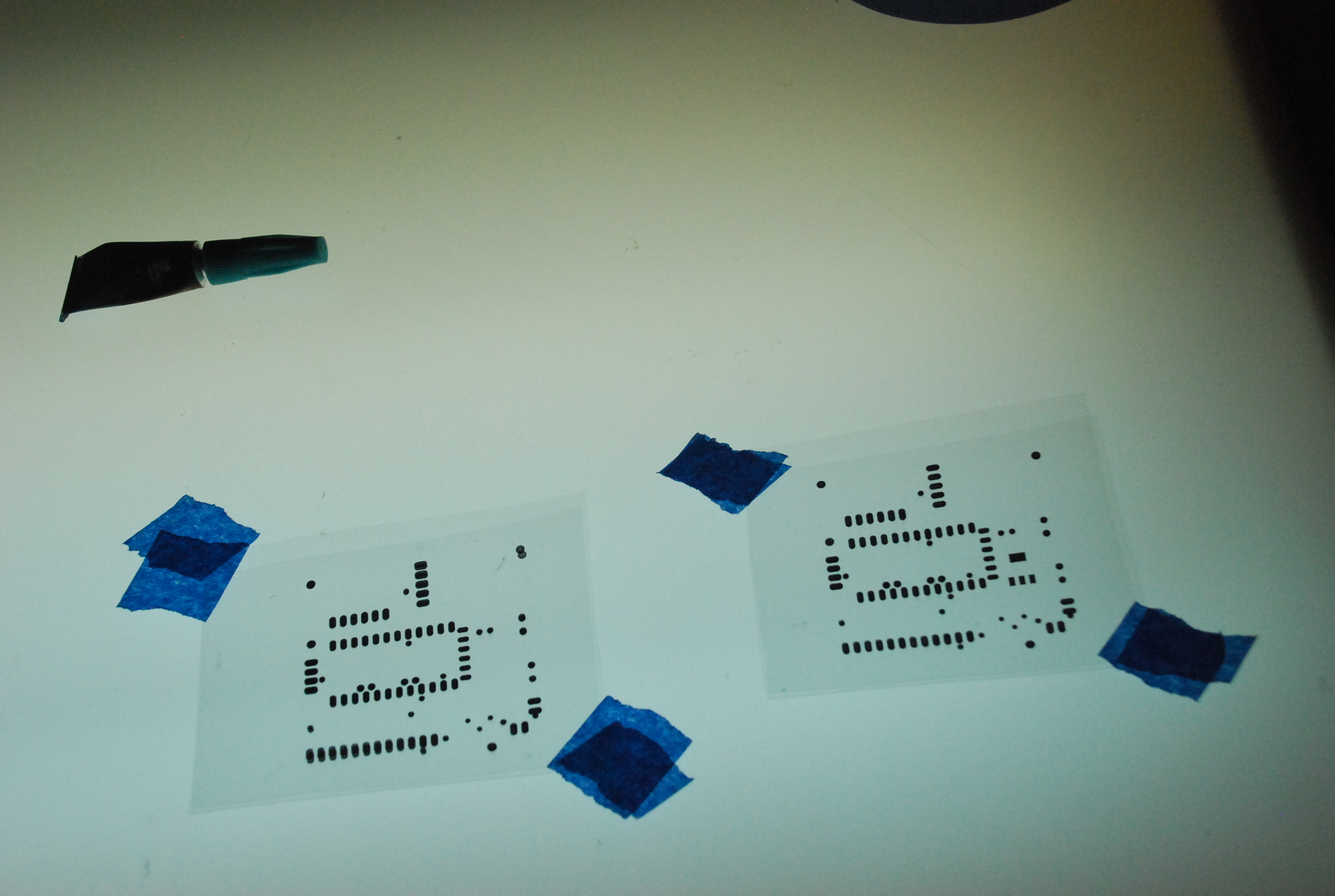
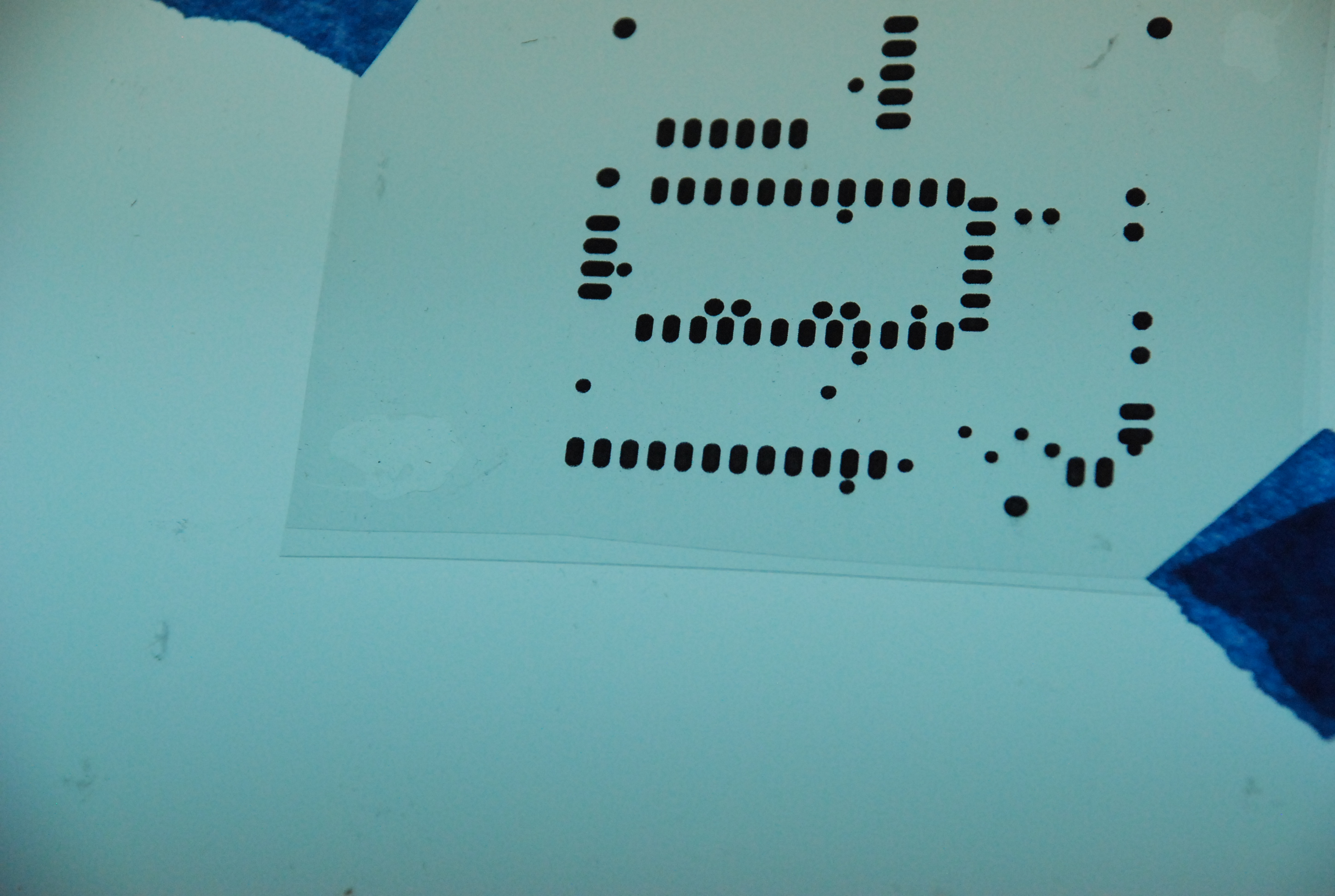
Once the board is dry, it is time to apply a Solder mask. This is an optional step but it will help to protect the copper from oxidation , looks more professional and improves the SMD component placement.
Again since the description of this process does not convey all the nuances necessary for success I have included a video.
Film mask is hard to find and very expensive so I use the tubes of UV curable solder mask obtained from various sources on the internet. No matter if you use film or paint you will need a source of UV light. I built a UV Exposure Unit using a roll of Purple/UV LED strips.:
It is important for protection of your eyesight that the UV source be enclosed inside a light tight box. There are many directions for the construction of other UV exposure devices on instructables.com, build one suitable for you. I use an electronic timer capable of seconds measurement and activating a relay to turn on and off the DC current to the UV source.
Since Laser printers do not print an image of sufficient density, you'll need to combine 2 images. Cut out two copies of each solder mask from the film and carefully align them to form the mask for each side. I permanently glue them together with a small dot of "Super Glue" on opposite corners away from the printed image.
The next step is most heuristic and will require testing your exposure setup (see instructions below) as well as some experimentation with your paint application.
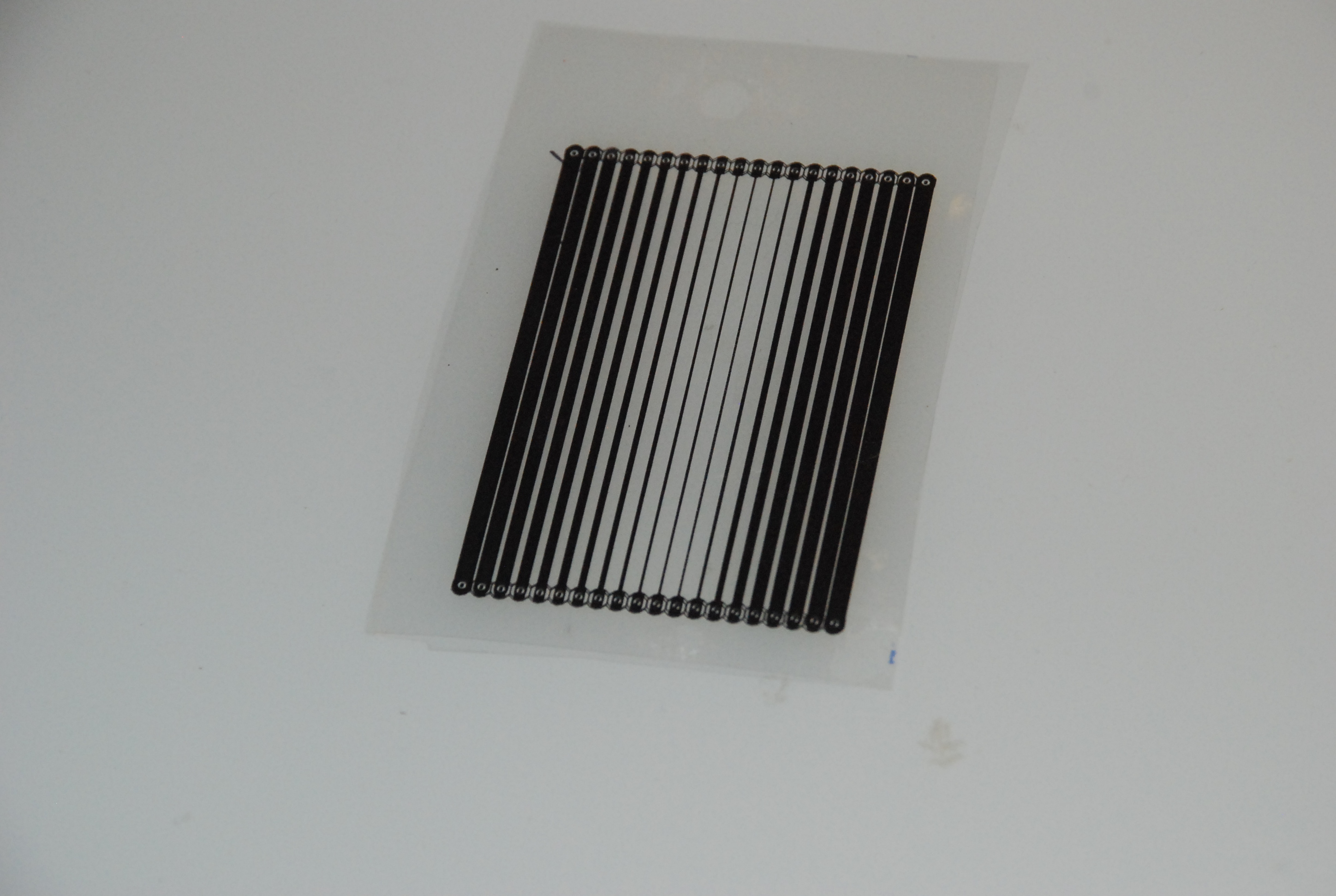
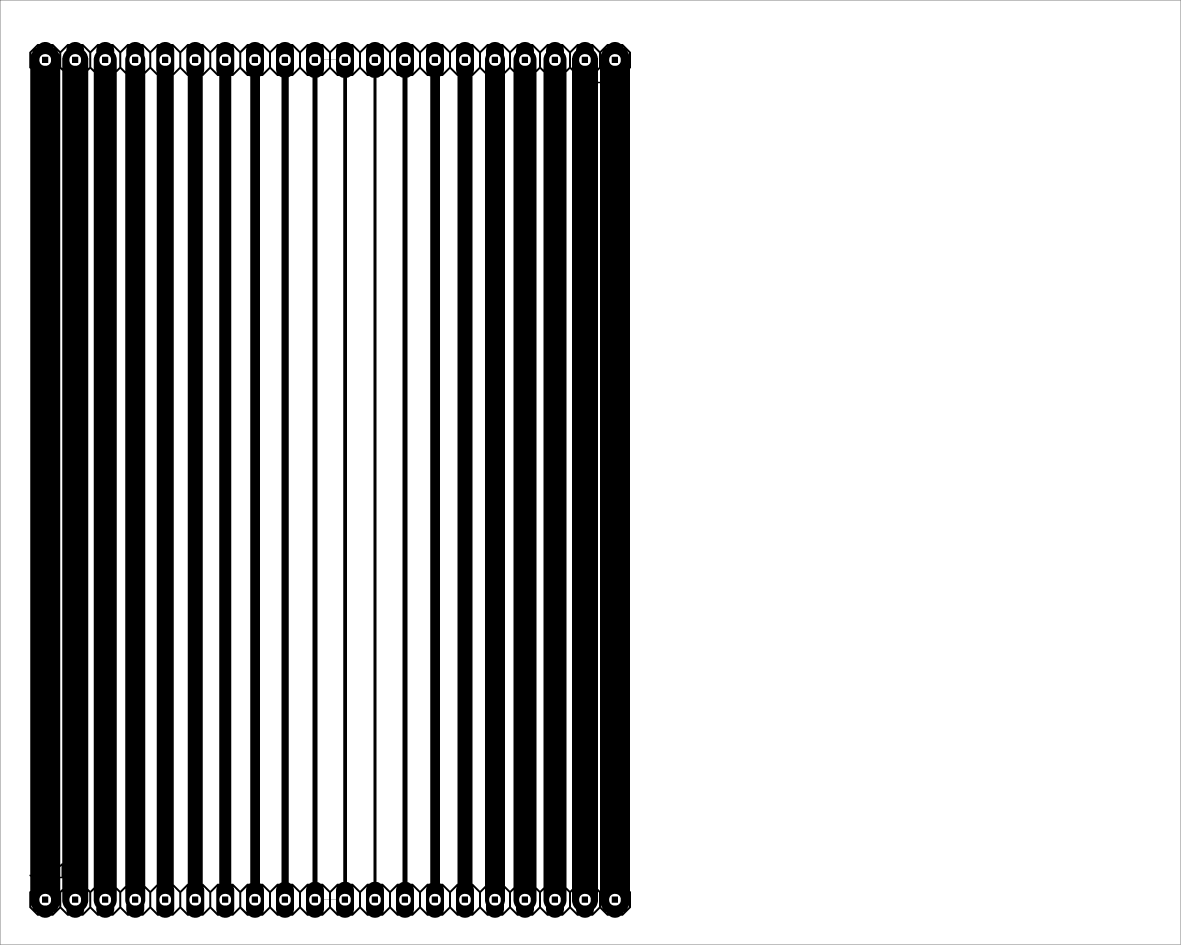
Testing your UV exposure device - I do not know what sort of UV levels your device will output or your paint thickness, there are just too many variables. You need to establish the exposure timing suitable to your particular setup and paint density. To do this prepare a sample exposure guide and cover a blank PCB board with paint following the below instructions ( I have attached a striped exposure image which you can print on acetate and use as your test mask don't forget to double up and glue it).
Start out with a time of 10 minutes total, divide it into four 2 1/2 minutes periods and expose a sample board moving a piece of carboard each 2 1/2 minutes so that one segment is exposed for 2 1/2 minutes next for 5 minutes, then 7 1/2 and finally the full 10 minutes. Remove and clean the board using paper towels and paint thinner to see which areas became hard and which have not. If it is almost all hard or all removed, double or half the times and try again with a clean piece of PC board. Use these timings to determine a suggested exposure time for your first board.
Warning! Once the mask has hardened it is almost impossible to remove, determine your exposure times carefully before committing your circuit board to this process. If you are consistent in preparing your boards you should not have to change the exposure times.
Using the timings you derived from the test, expose your mask. After exposure of your finished board remove it from the UV box, remove the solder mask and peel back the acetate cover sheet. You should see the paint sticking to this sheet where the pads appear on your mask but not elsewhere on the board . Now using paper toweling and remove the unexposed paint with paint thinner. All the paint should be removed from the copper pads and vias but not the traces, clean the board back and front and dry with paper toweling. To finish hardening your mask first inspect the unexposed areas and using sharp tool remove any paint from unwanted areas. Then place the board in your UV exposure box and expose for at least twice to 3 times the original exposure time. Process the second side, if needed, in the same manner.
Drill Your Board
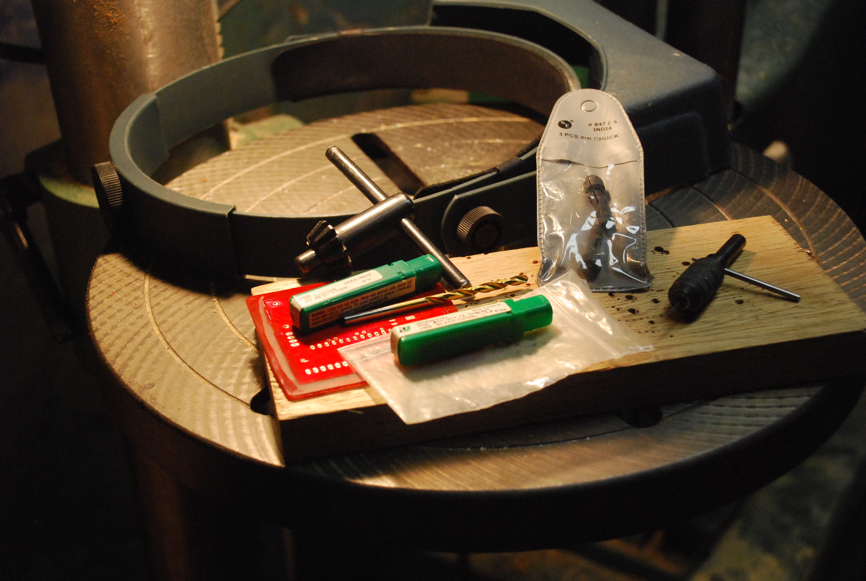
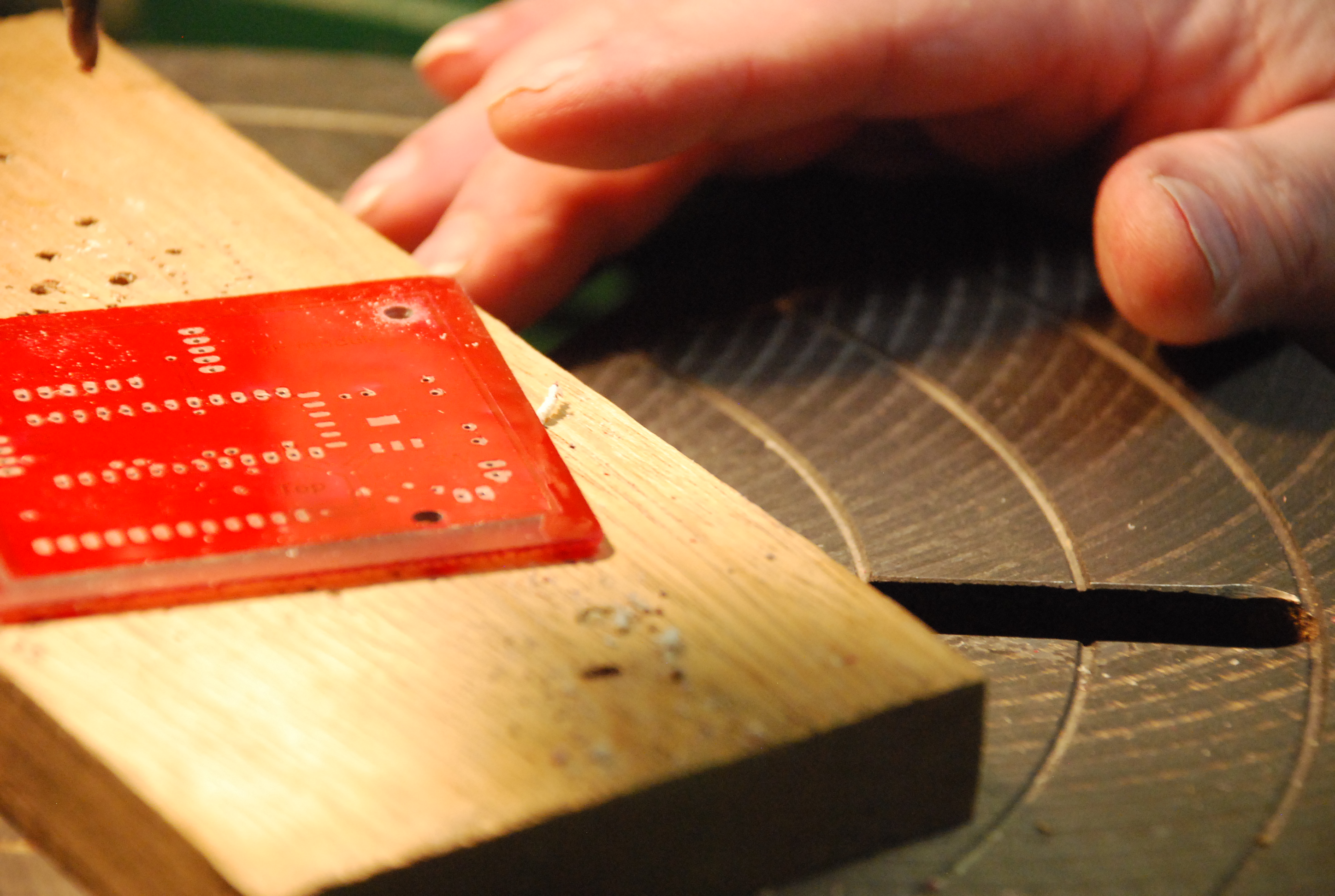
Drill out the holes for vias, through-the-hole components and mounting holes. I use a drill press with a drill vice for the wire size bits. I find that the board is easier to handle if it is drilled before cutting to final size.
Cut to Final Size
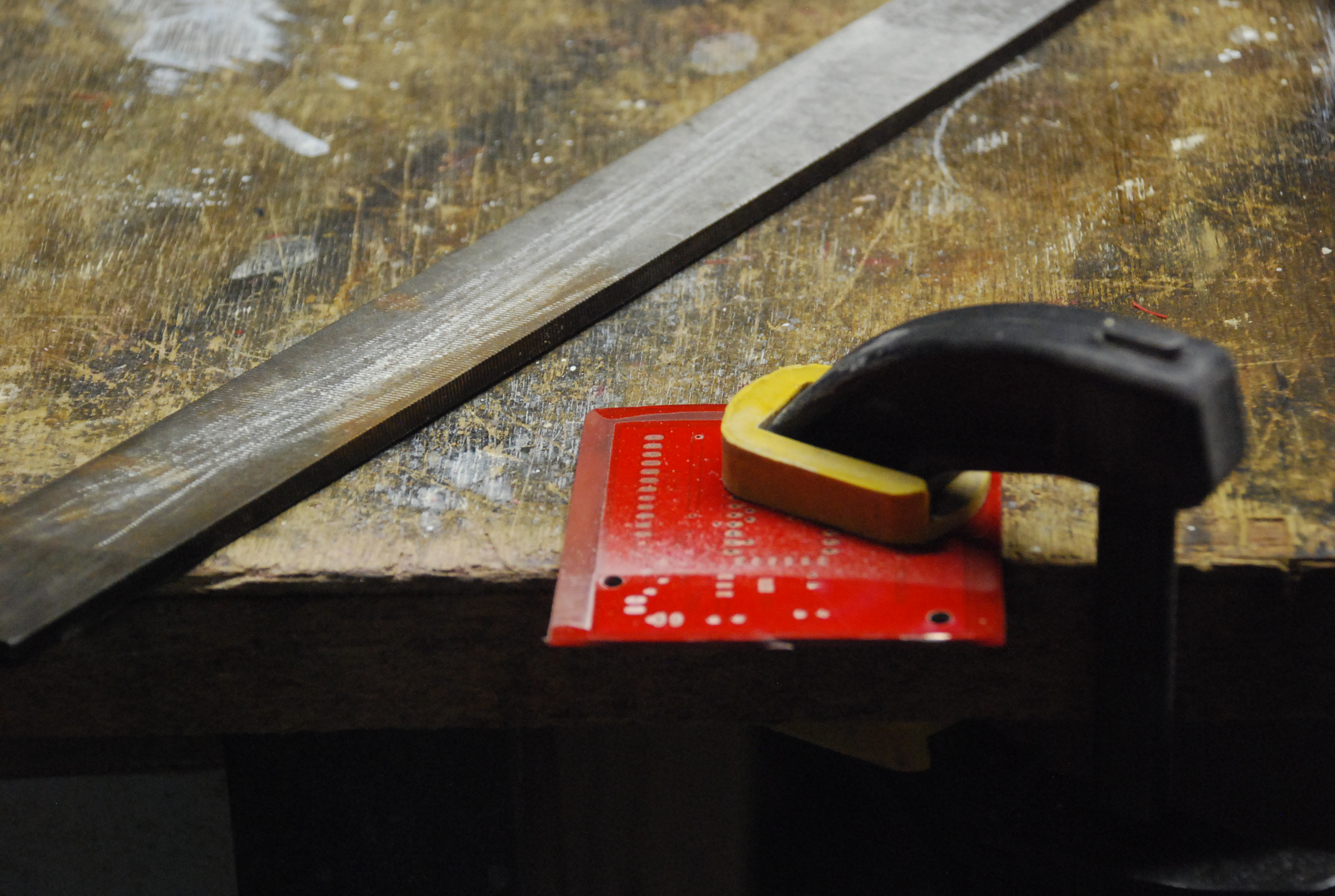
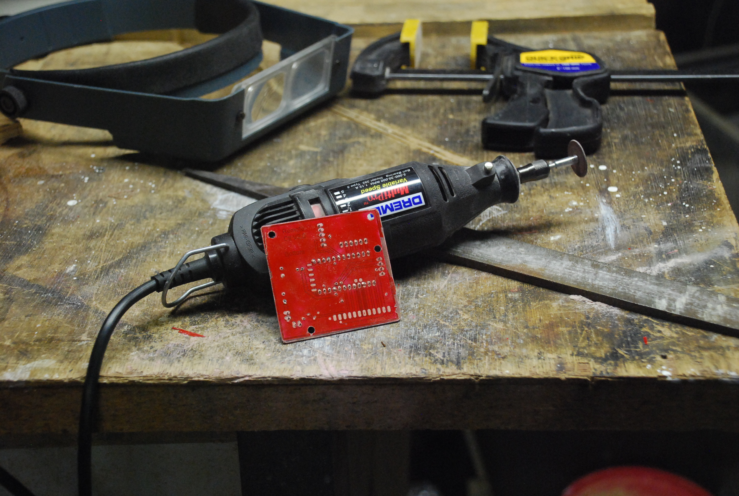
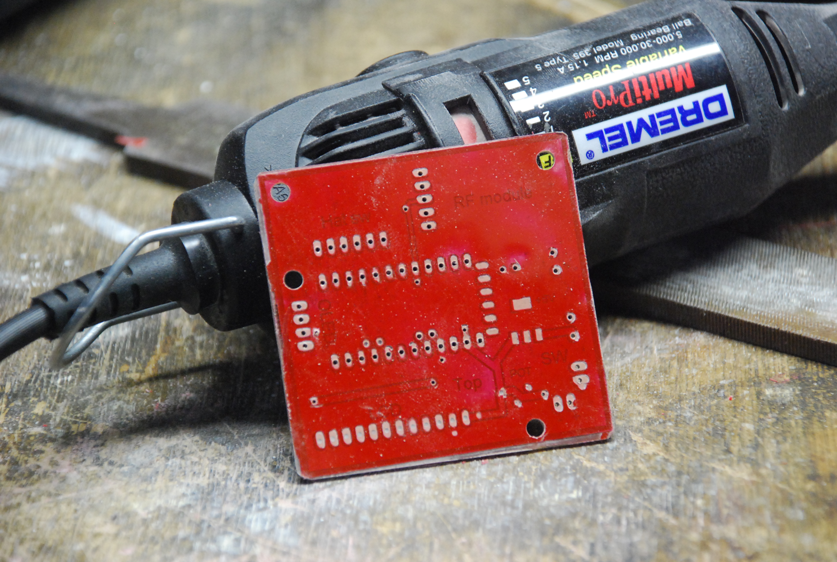
Using the board profile lines as a guide, trim the board using a rotary tool and cutoff wheel, File edges and round corners
Populate Your Board
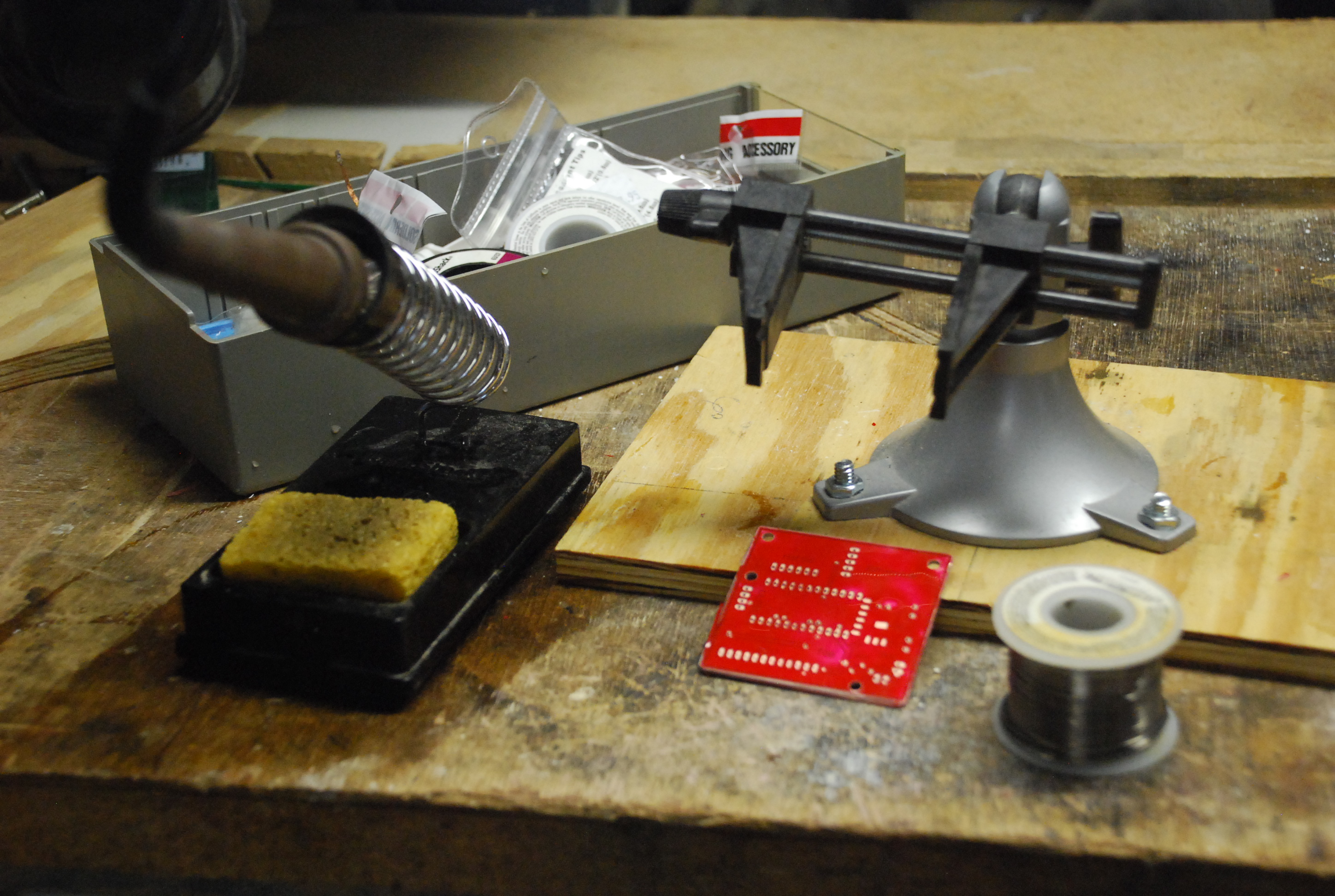
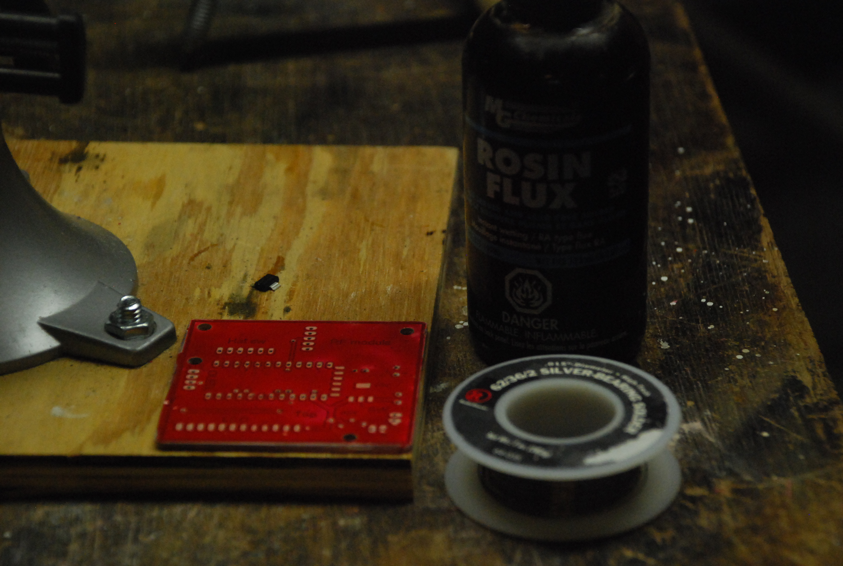
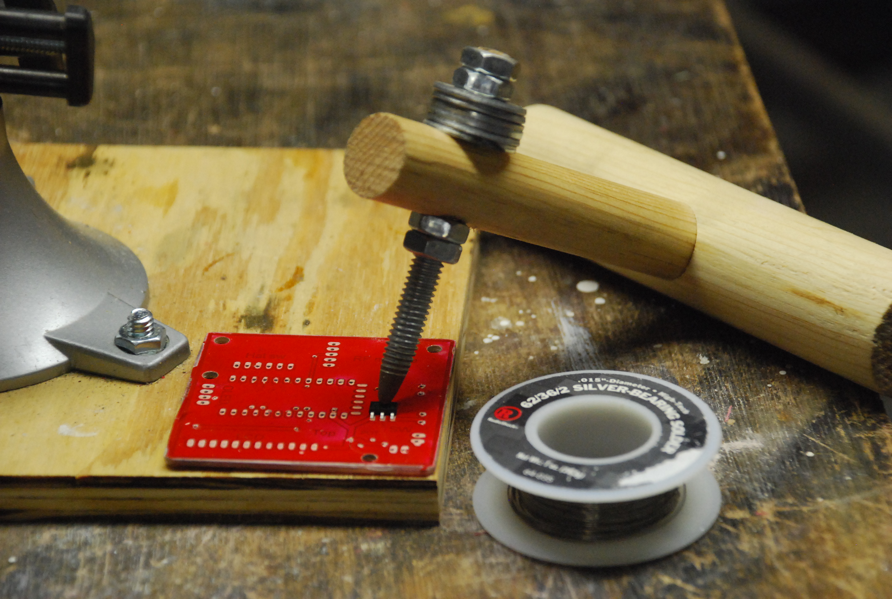
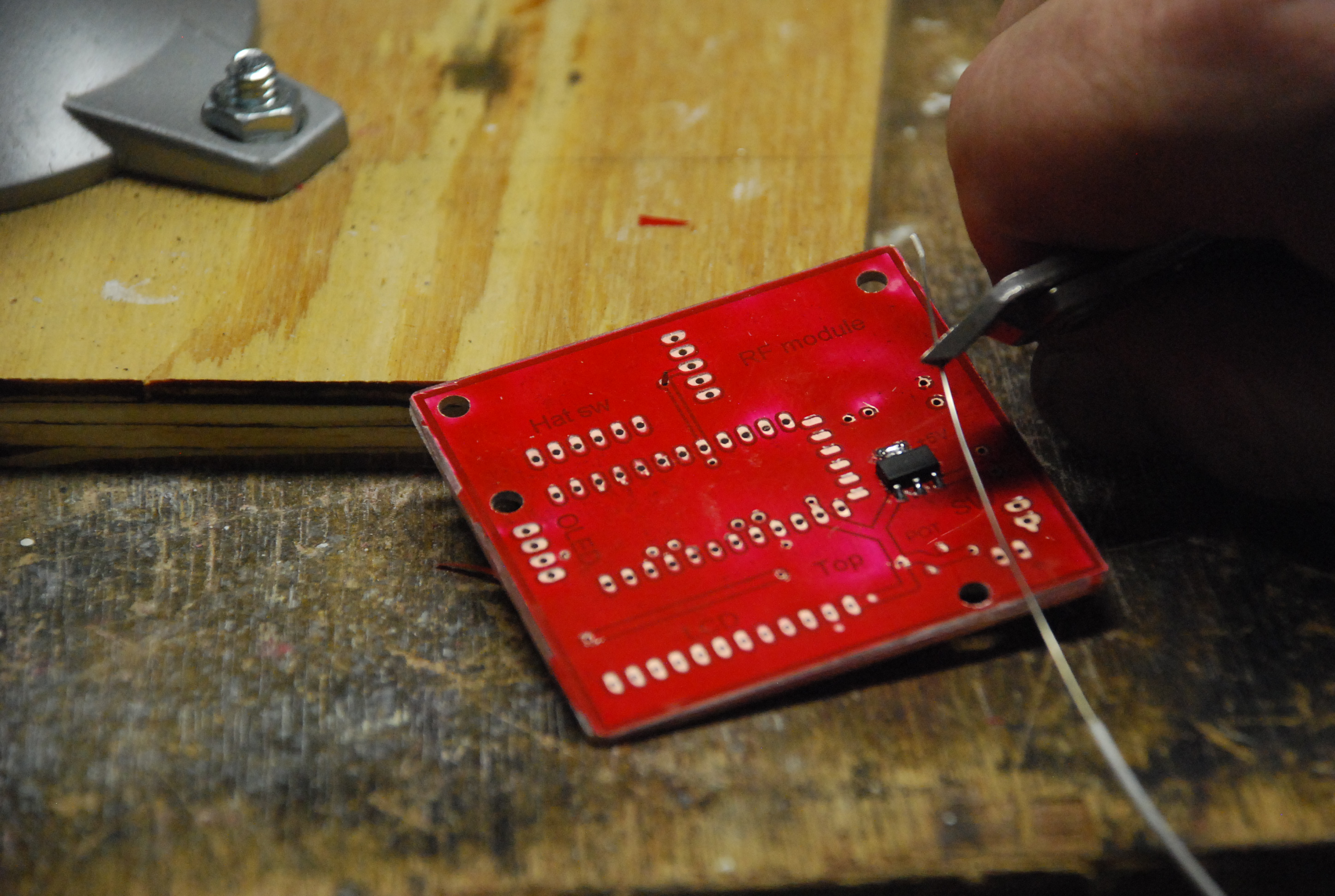
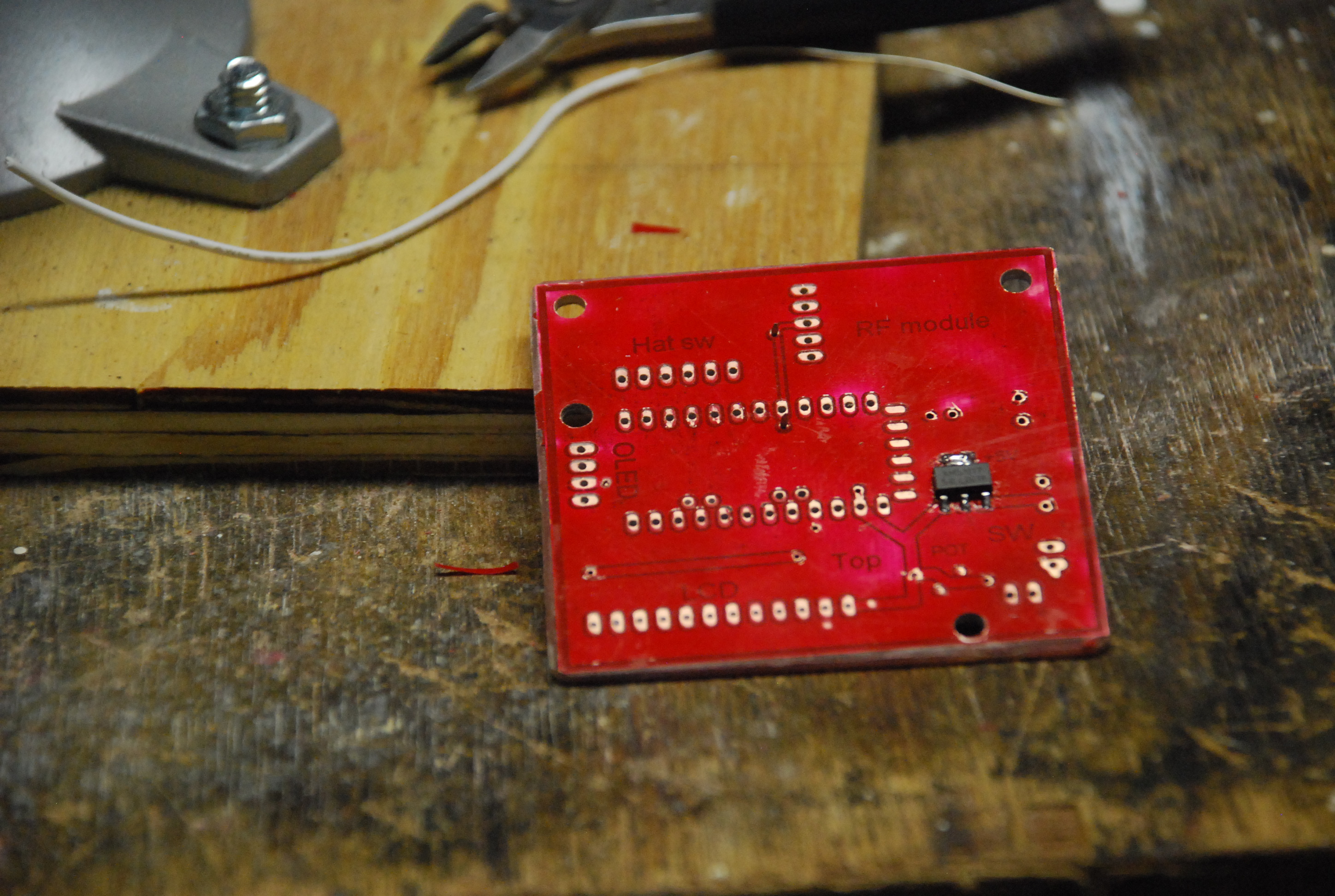
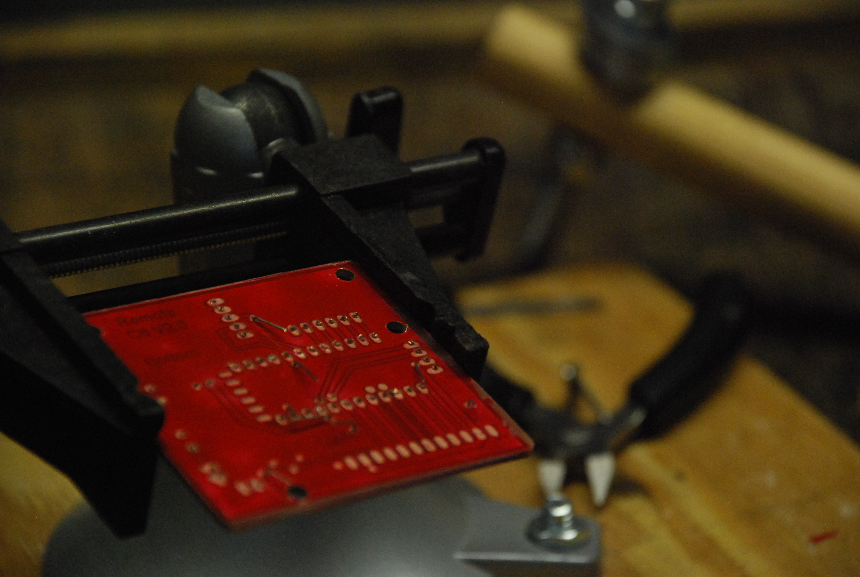
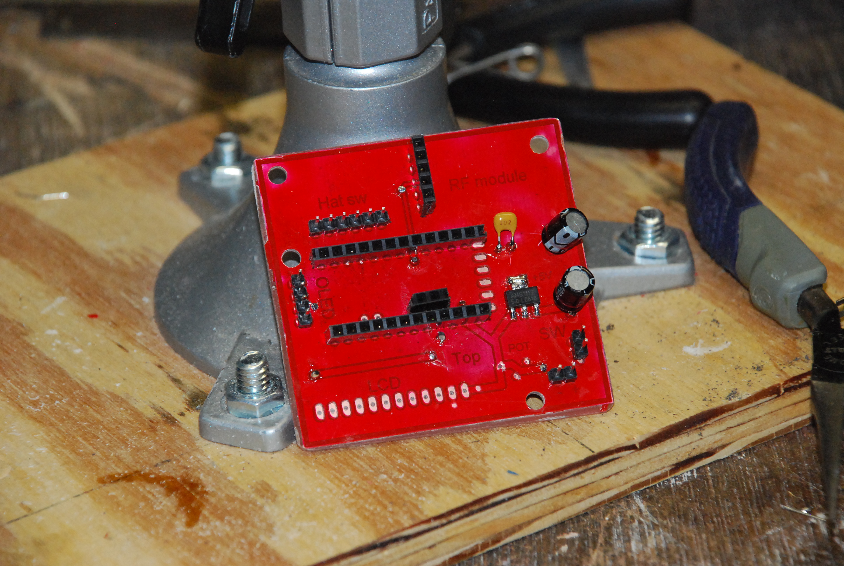
I usually hand solder the SMD parts first, then the vias and finally through-the-hole components.
I made this device to hold down SMD components when soldering from couple of dowels some washers boles and nuts. I apply a little liquid flux to the SMD pads hold the component down then solder in place.
A trick for the vias is to flatten a bit of the wire end with a pair of plyers so they do not drop through the via hole. Solder on the front side then bend the wire over and solder on the back.
Your board is complete and ready to test.
I hope this instructable though long was helpful. Please feel free to provide constructive comments or ideas.
Thanks for taking the time to look at my process and have fun building your electronic projects.