Building an SMD PCB Stencil and Frame With Eagle Software
by HomeCSP in Circuits > Electronics
6071 Views, 17 Favorites, 0 Comments
Building an SMD PCB Stencil and Frame With Eagle Software
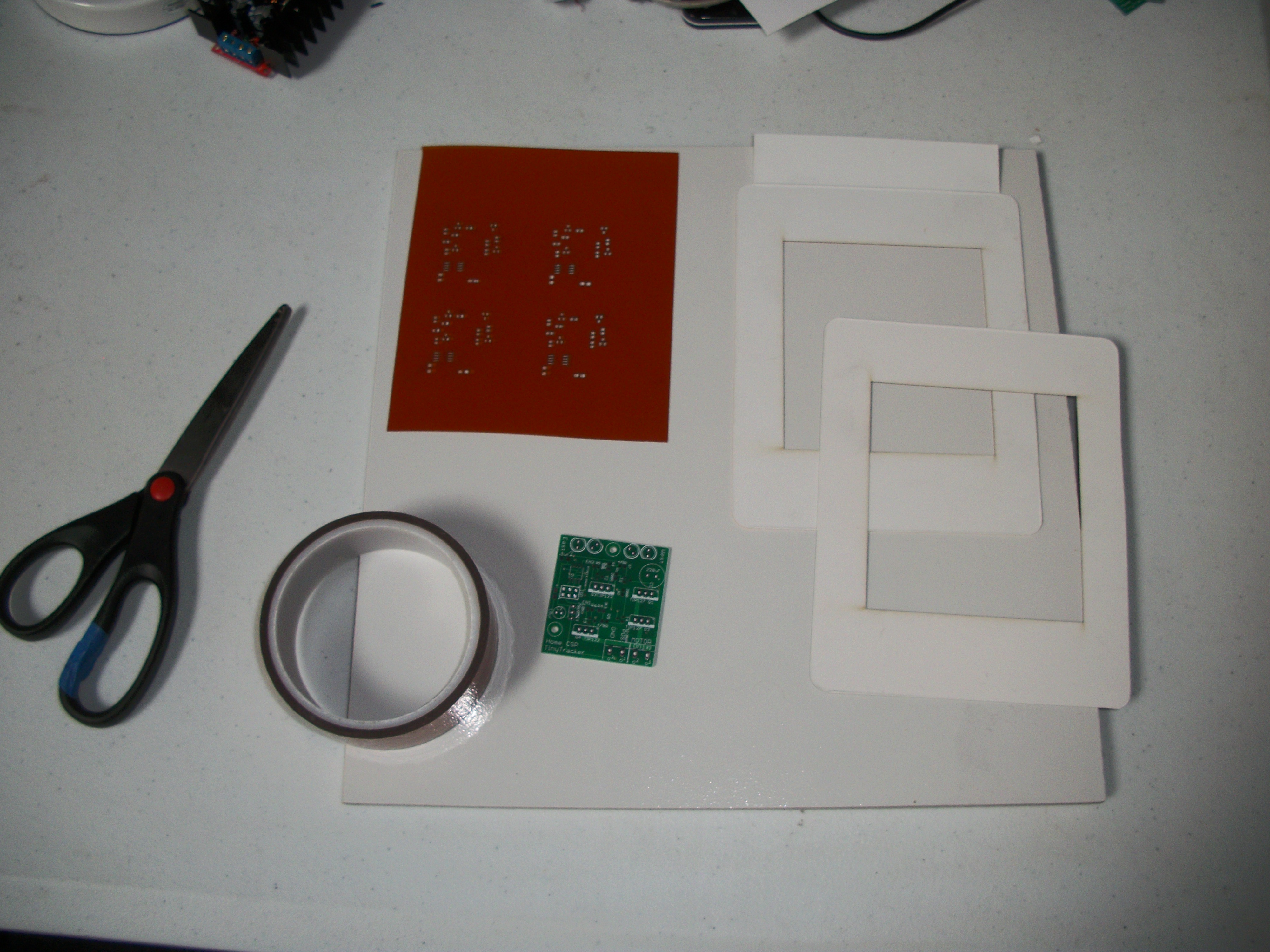
There are several articles that discuss DIY stencils, but I couldn't find any that covered using stencil with a frame. I make lots of pcbs that are 5x5cm or smaller. Since they are so small, it's nice to do several at once. Commercial entry level stencil frames cost hundreds of dollars. CadSoft's Eagle software is very popular within the Arduino community, and is ideal for creating small pcb prototypes. With a cheap and easy to use stencil setup, even hobbyists can due small smd board runs and save the tedium of applying solder paste with a needle. This Instructable covers steps for creating a 4-up stencil and making a simple jig with tape and cardboard to assist the stencil paste application process. Stencils are now commonly available from pcb manufacturers online, but you can save a lot of money making them yourself if you have access to a laser cutter. For this project, I made it at TechShop on a Trotek laser. Total project time required was around 1 hour. Main skills required are basic vector artwork editing using Corel Draw or similar software.
Materials Used:
5 mil Kapton film
1 mil Kapton Tape
12" white Ceramic Tile
2 pieces of Cardboard (recycled)
The extra thick Kapton film is available for about $35 for a 12x12 square, which is ample for several stencils. Some people use wide tape and clean the adhesive layer off. Mylar and other thin films compatible with your laser cutter may also be substituted.
The ceramic tile are cheap, available individually for about $1 and make a nice project base.
Key aspect of cardboard selection is that two layers of the cardboard are slightly thinner than your pcbs. I used some recycled product packaging inserts that were ideally sized.
One piece of cardboard will act as a frame to hold the pcbs, while the other will hold the Kapton stencil and be hinged above the first. You can cut both of these from a single larger piece if that's what you have.
Making a Stencil From Eagle
Once you've finished your PCB design, it's easy to use Eagle's command line functions to create .EPS files you can use to create the stencil.
I put the following in a little file named Stencil.bat
"C:\Program Files (x86)\EAGLE-6.2.0\bin\eagle.exe" -X -dEPS -o%1.Outline.eps %1.brd 20
"C:\Program Files (x86)\EAGLE-6.2.0\bin\eagle.exe" -X -dEPS -o%1.TopStencil.eps %1.brd 20 31
Change these lines if you've installed Eagle to another location. Save the Stencil.bat file to the folder with your Eagle schematic and board files.
Open an old fashioned Command Prompt window and navigate to the folder with your files (use the CD command), then type in a command like:
Stencil MyBoardV1
If everything goes right, you'll find the two .eps files (MyBoardV1.Outline.eps and MyBoardV1TopStencil.eps) now created in the folder. These will be used by the vector based drawing program that prepares the files for the laser cutter.
Preparing Vector Artwork for the Laser Cutter
Part of the point of using a stencil is to make it easy to make lots of boards easily. In this example I arrange 4 pcbs together in a square.
Tips for editing vector artwork:
Open the TopStencil.eps file
Border and mounting hole lines may not be visible, you may need to temporarily change line widths. Start with a Select all operation to help see what's there.
Delete any mounting holes.
Select all of the solder pads, and change the fill to None, then change the line width to hairline and color to Red (for Trotek lasers anyway).
At this point I prefer to do the following: Select All, Group, Copy, Paste, carefully select the pasted group and it to the side, aligning the top left corner of the copied group with the top right corner of the original. Paste again, and this time align the top left corner of the new group with the bottom left corner of the first group. Paste one more and fill in the last copy in the lower right position for a 4-up layout.
Open the Outline.eps file follow similar steps as before to create a matching 4-up layout. This time delete all lines from the interior of the resulting bounding rectangle.
Use the laser cutter to make two copies of this on the cardboard pieces.
I trimmed my cardboard so that one piece had a small tab to act as a hinge, but you can make the hinge from tape just as well.
Now you can "print" the files to the laser printer.
Cutting the Stencil
The laser software I'm familiar with separates the artwork into layers based on color. Each layer has its own laser settings for cutting or etching. Make sure your material settings are set to Cut on the Red layer matching the stencil pads, and Skip the black outline layer.
First print should be done on a piece of paper to verify that you've got the stencil and job options set correctly.
Once you're satisfied with the results on paper, prepare your Kapton sheet. At this point it's nice to pic something like a single SOIC footprint or similar fine detail from your stencil design and create a new file for it. Sacrifice a small corner of your Kapton film to verify your power settings with the small detail before moving on to the actual stencil job.
Tip: a few scraps of acrylic can help hold the Kapton film edges down for a more consistent laser focus distance which helps for better results.
Making the Stencil Frame
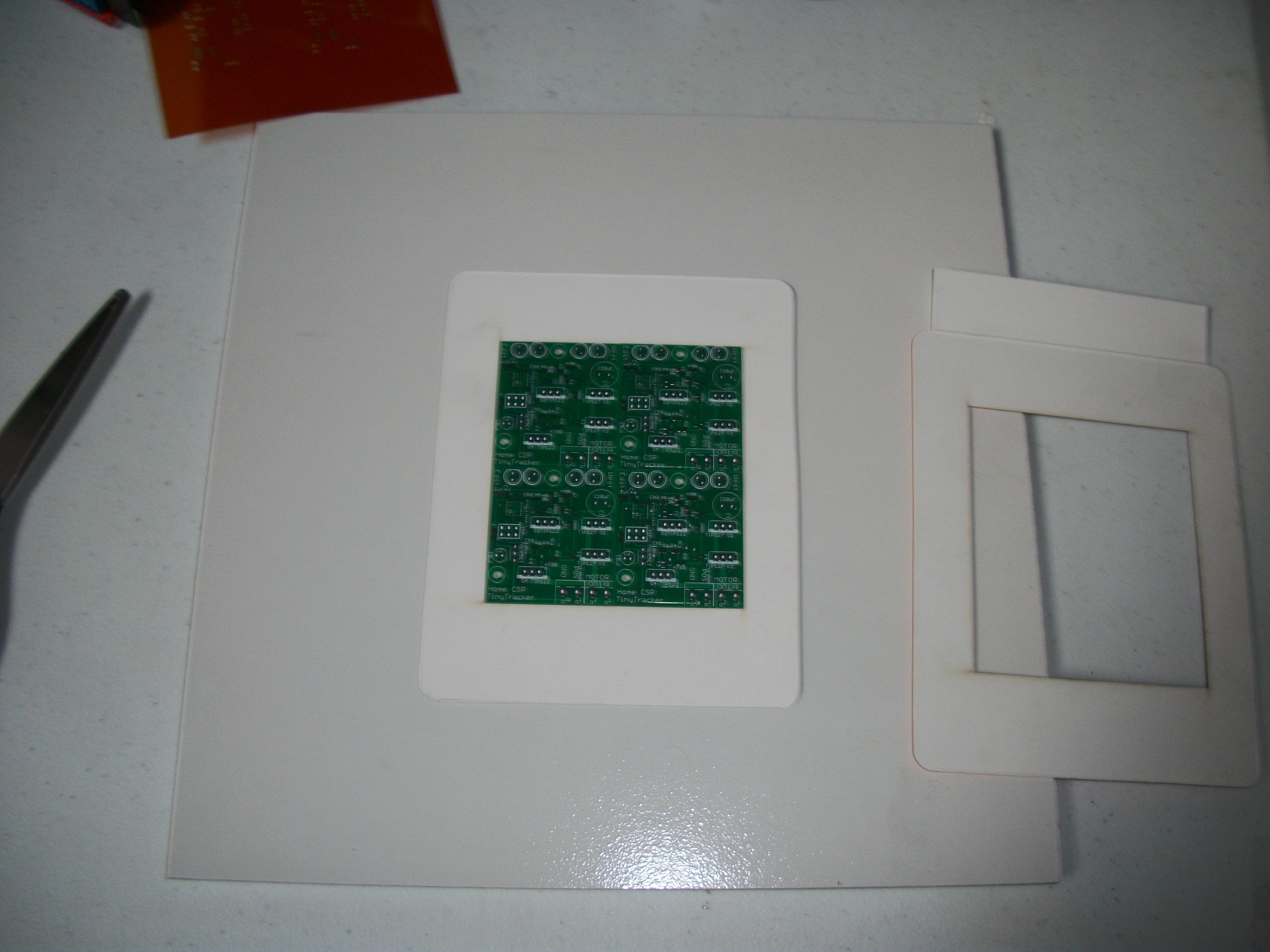
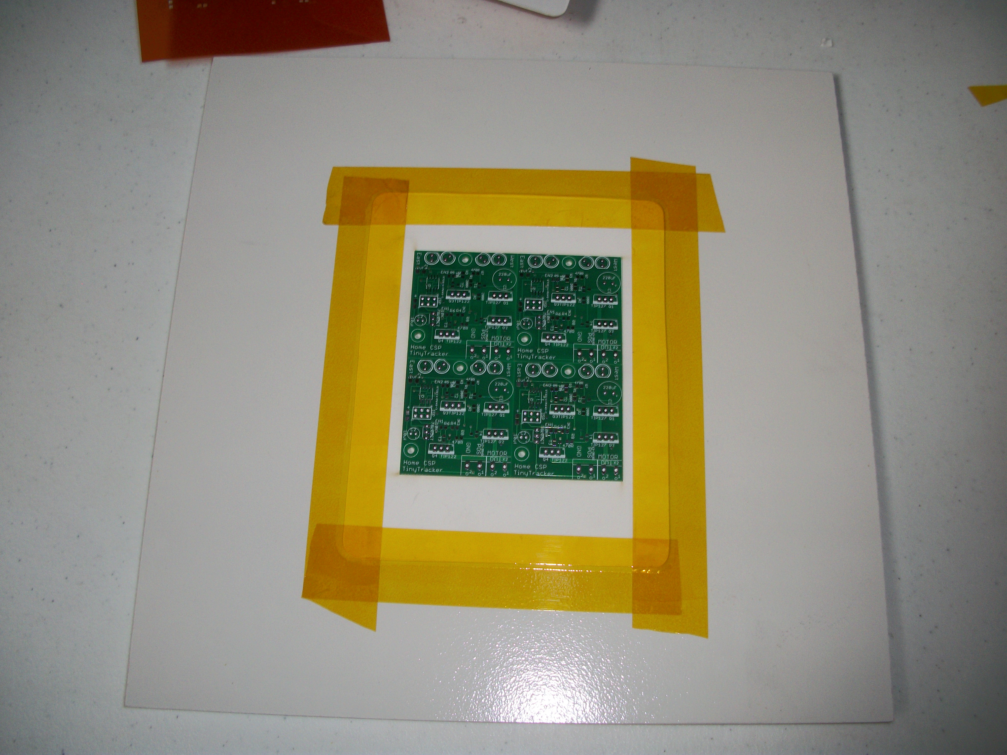
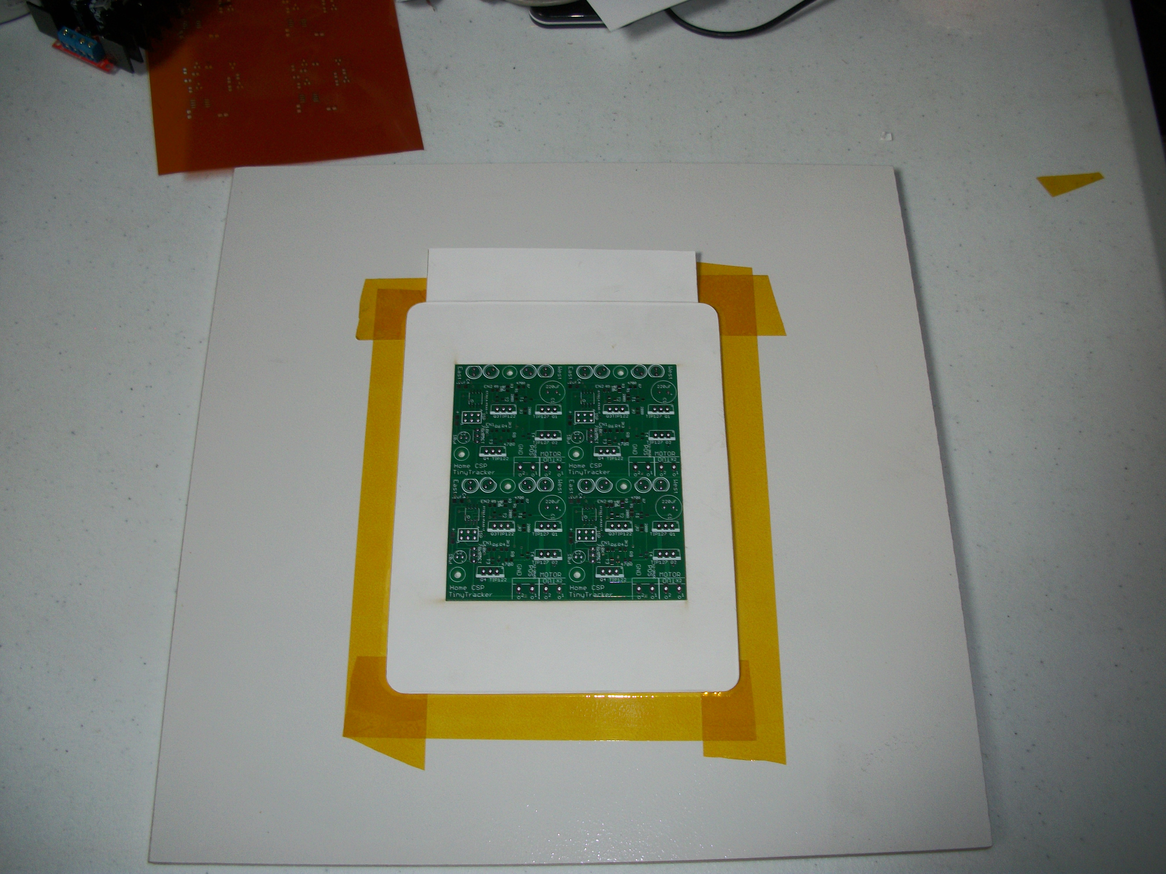
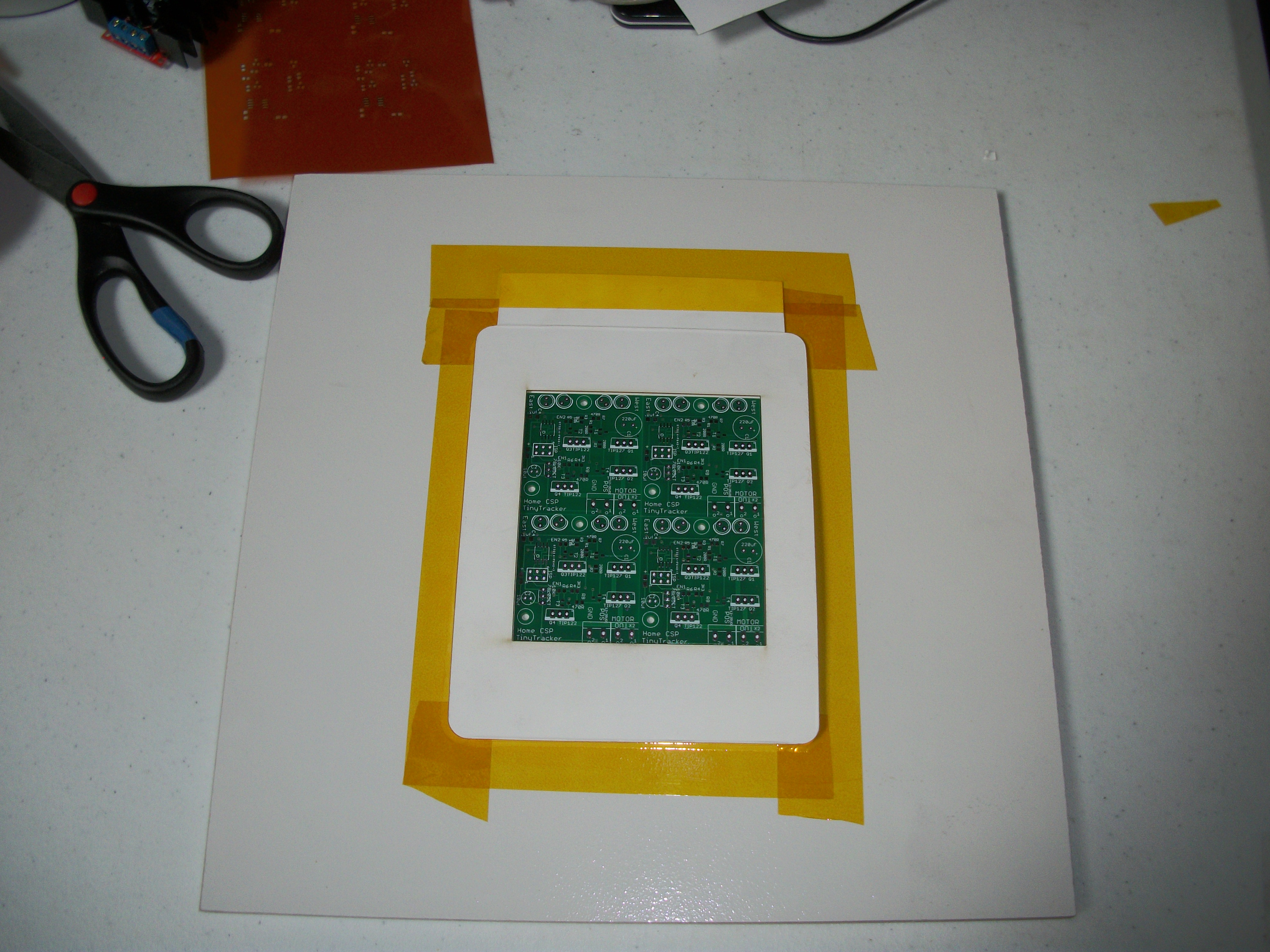
Align the bottom frame piece on the tile, and carefully tape it down. Sealed edges help keep things tidy in use.
With the base frame in place, arrange your pcbs inside.
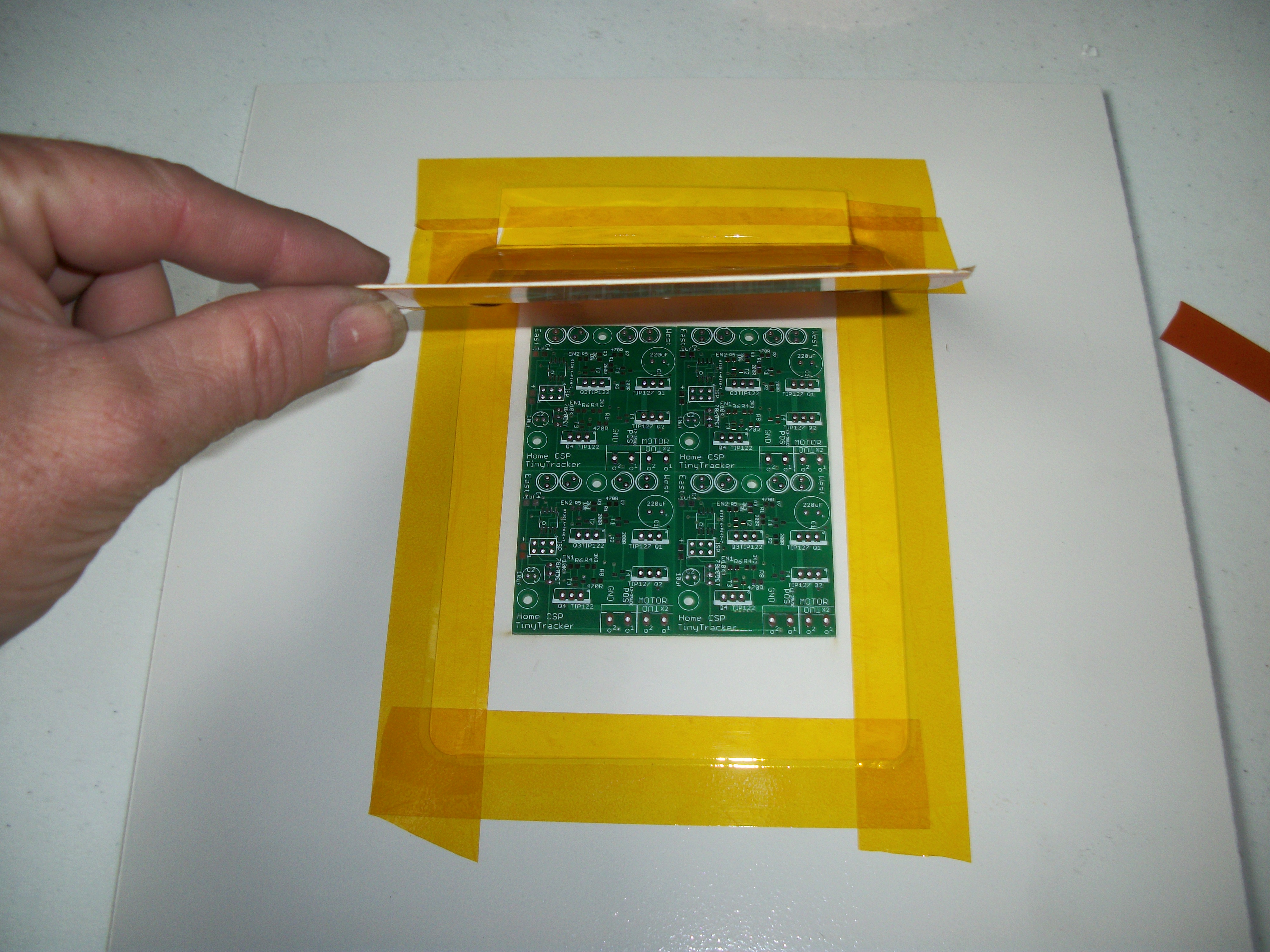
Place the hinged frame on top and with the two pieces aligned, tape just the hinge down to hold it in place.
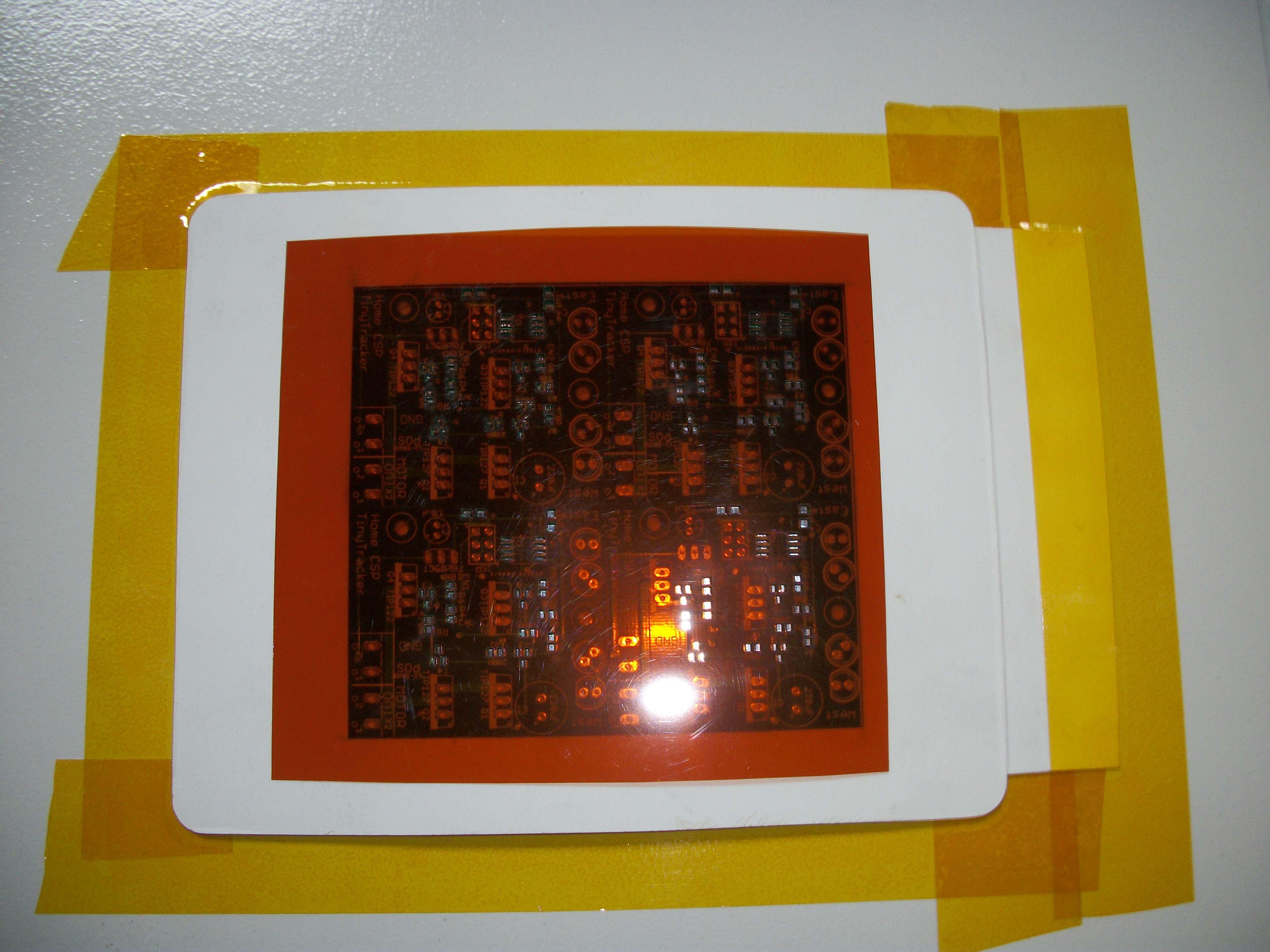
Now hold the stencil on top and align it with the pcbs.
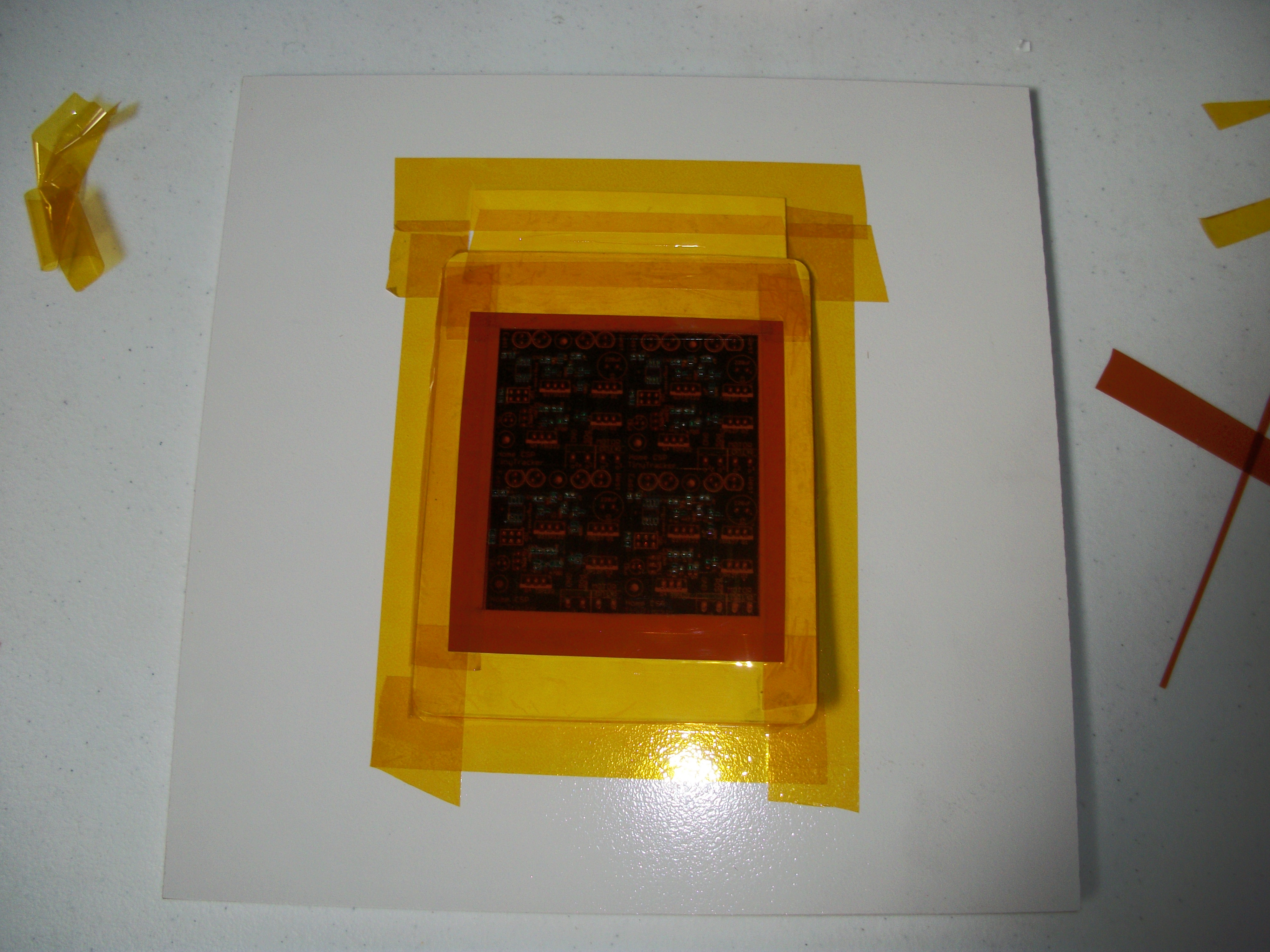
Trim the stencil if necessary so it fits in the middle of the frame edges, then carefully tape it down. It's important to start at the bottom, then do the sides, and then the top last. I fold the tape over the edges to provide a nice sealed edge to make cleanup easy. When drawing the paste down the stencil this will help prevent the edges of the tape from lifting or getting paste underneath.
Once all done it should be easy to hold the stencil down on the pcbs while applying paste, and then to lift the frame and remove/replace the pcbs.