Basics: How to Design & Fabricate a PCB Using EAGLE
by Rehaan33 in Circuits > Electronics
24840 Views, 232 Favorites, 0 Comments
Basics: How to Design & Fabricate a PCB Using EAGLE
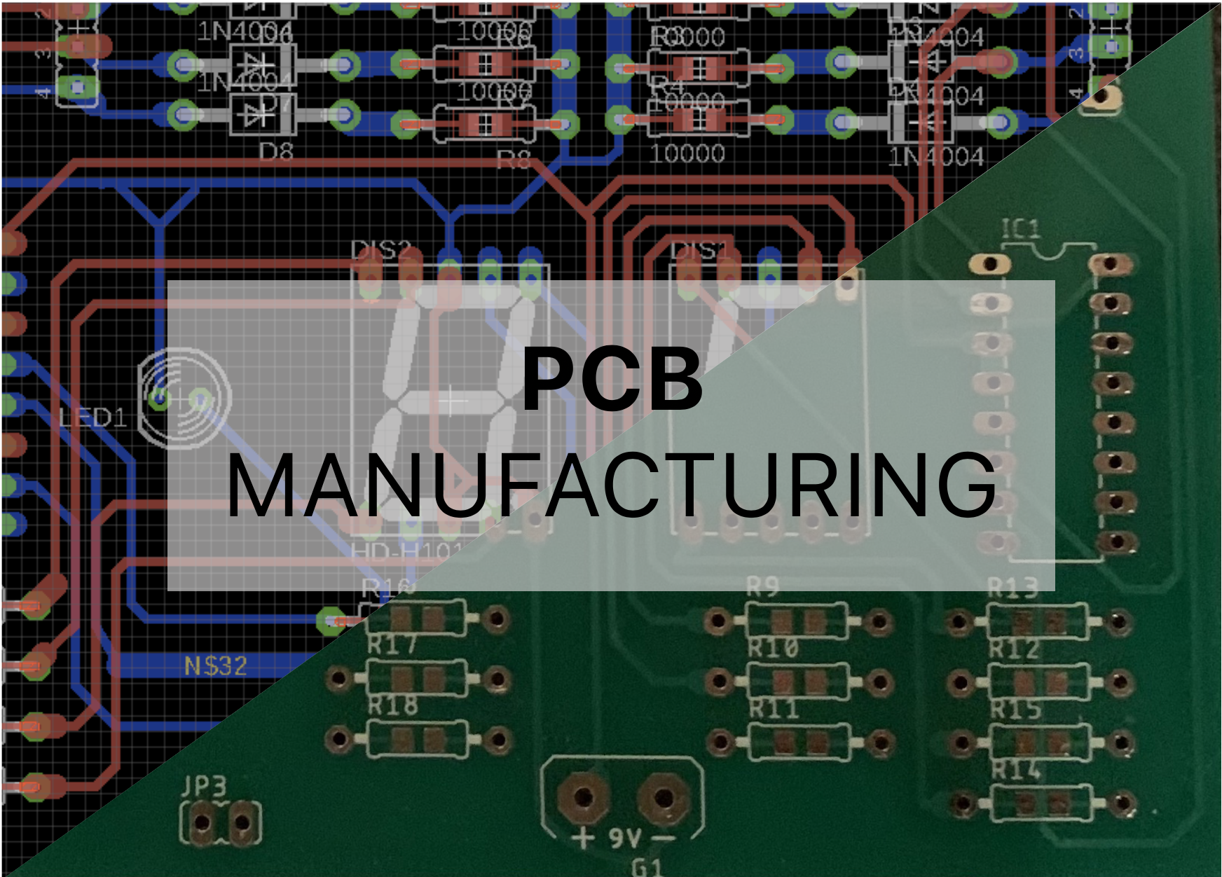
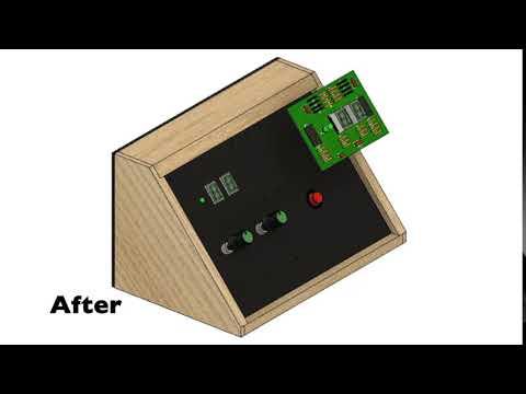
PCBs are used in devices all around us. As shown in the short video above, they help organize and keep circuits as compact and efficient as possible. Designing and manufacturing your own might seem like a daunting task, but please do not worry. The process is neither complicated nor expensive.
In this Instructable, I will be going through the absolute basics of Eagle and how to design and produce a PCB from scratch. Having gone through this process as a beginner myself, I understand how complicated Eagle may seem to be and the number of errors you might run into. As such, I hope this Instructable is able to give you some grounding in using the software and confidence in having your custom PCBs manufactured overseas.
It is important to note that this is NOT a complete guide to Eagle nor do consider myself to be a professional with this software in any way. If you have any questions, please feel free to ask them in the comment section below.
You may begin by downloading Autodesk Eagle here.
Download Libraries
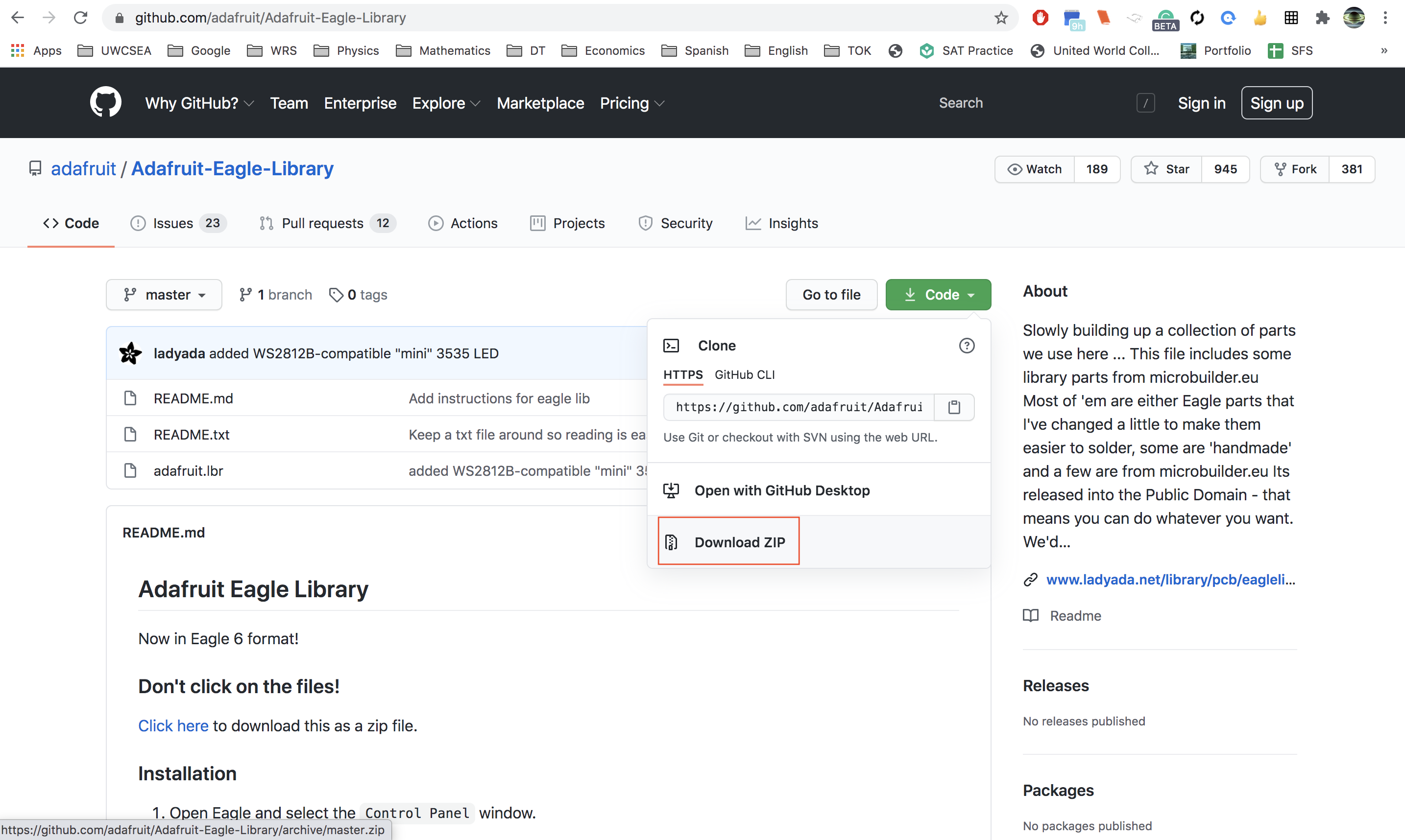
In order to proceed with Eagle, it is important to first download a few libraries containing the parts you expect to use in your schematic/circuit. The most important library to download first is the Adafruit GitHub Library. It is a good starting place if you are unsure of what library to use.
It can be found here
Once you are on the page, click on the green 'code' button, and then download the .zip file.
Add Libraries
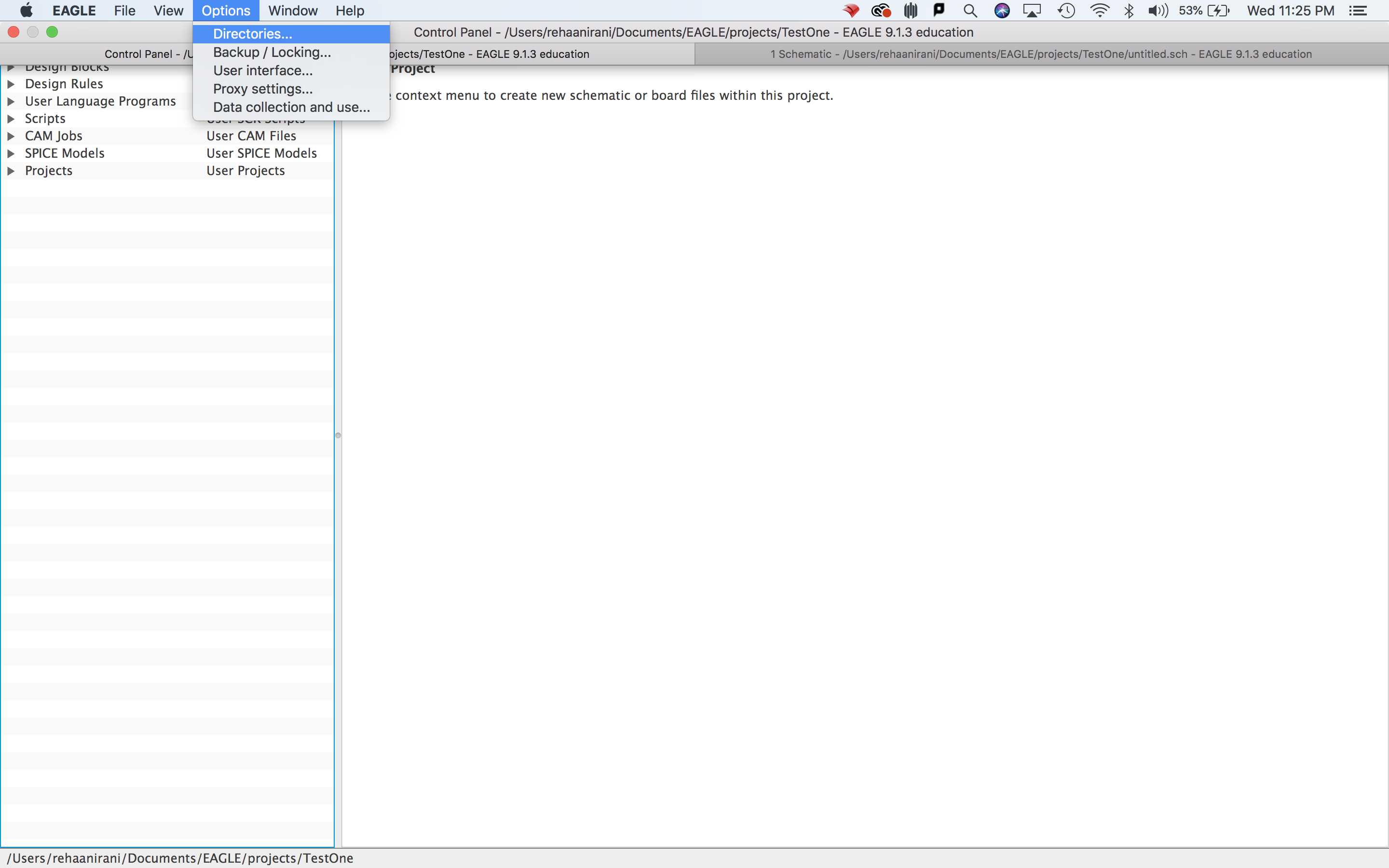
This step can be a little tricky. Once you unzip the file, you should be left with a folder (mine was named 'Adafruit-Eagle-Library-master')
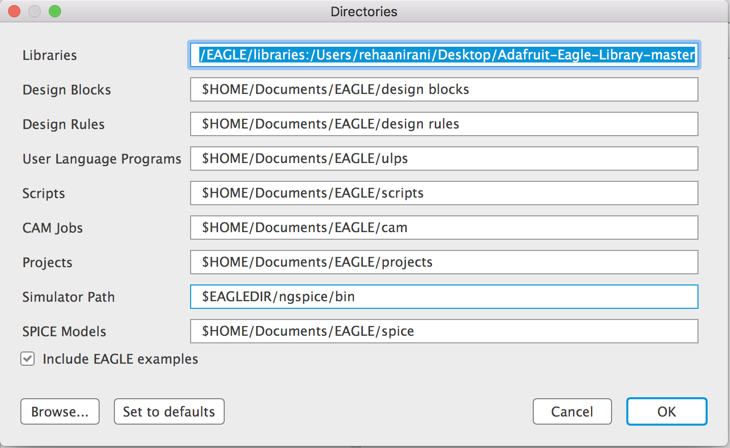
Now, open up Eagle, and head to 'Options', and then 'Directories'. You should now see the pop up displayed in the photo on the top right. In the libraries section, you might see something like this already written there (please do not delete this):
$HOME/Documents/EAGLE/libraries
In order to add the Adafruit libraries, we have to add the path to the folder to the text above (this website will show you how to find the path to your folder), separated by a colon. The path to my Adafruit folder is:
/Users/rehaanirani/Desktop/Adafruit-Eagle-Library-master
Therefore, I have to add this path to the original text as shown below (separated by a colon):
$HOME/Documents/EAGLE/libraries:/Users/rehaanirani/Desktop/Adafruit-Eagle-Library-master
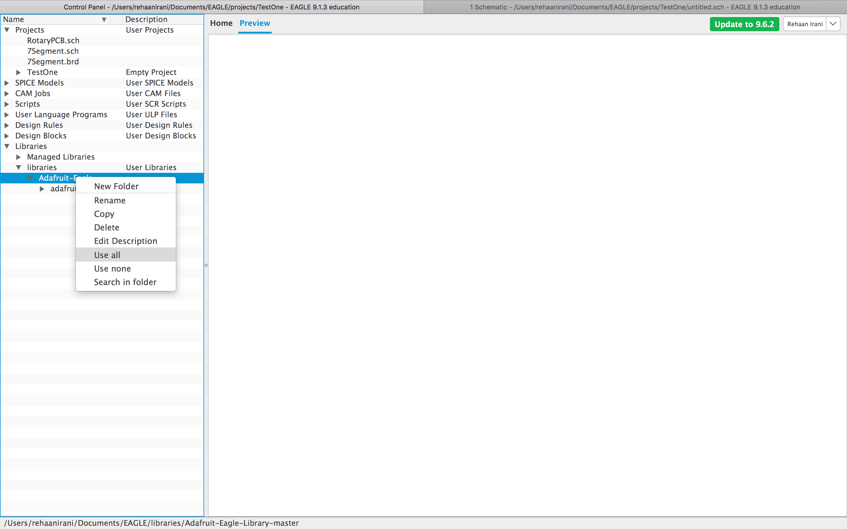
Once this is done, go ahead and click 'OK'. Once you go back to the main menu, under 'Libraries', you should see the Adafruit library. Make sure to right-click on it and select 'Use All'.
Create a New Project & Schematic
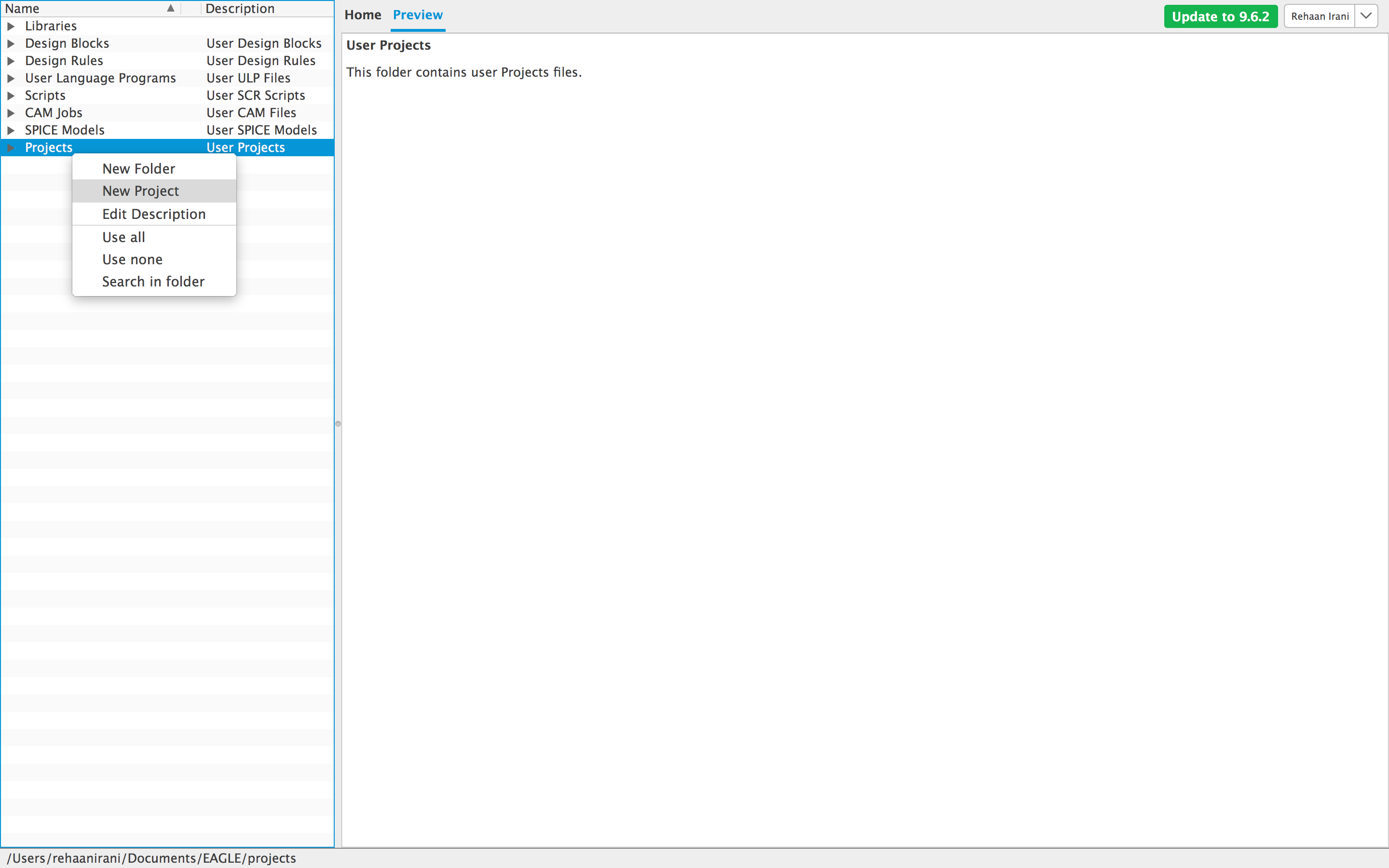
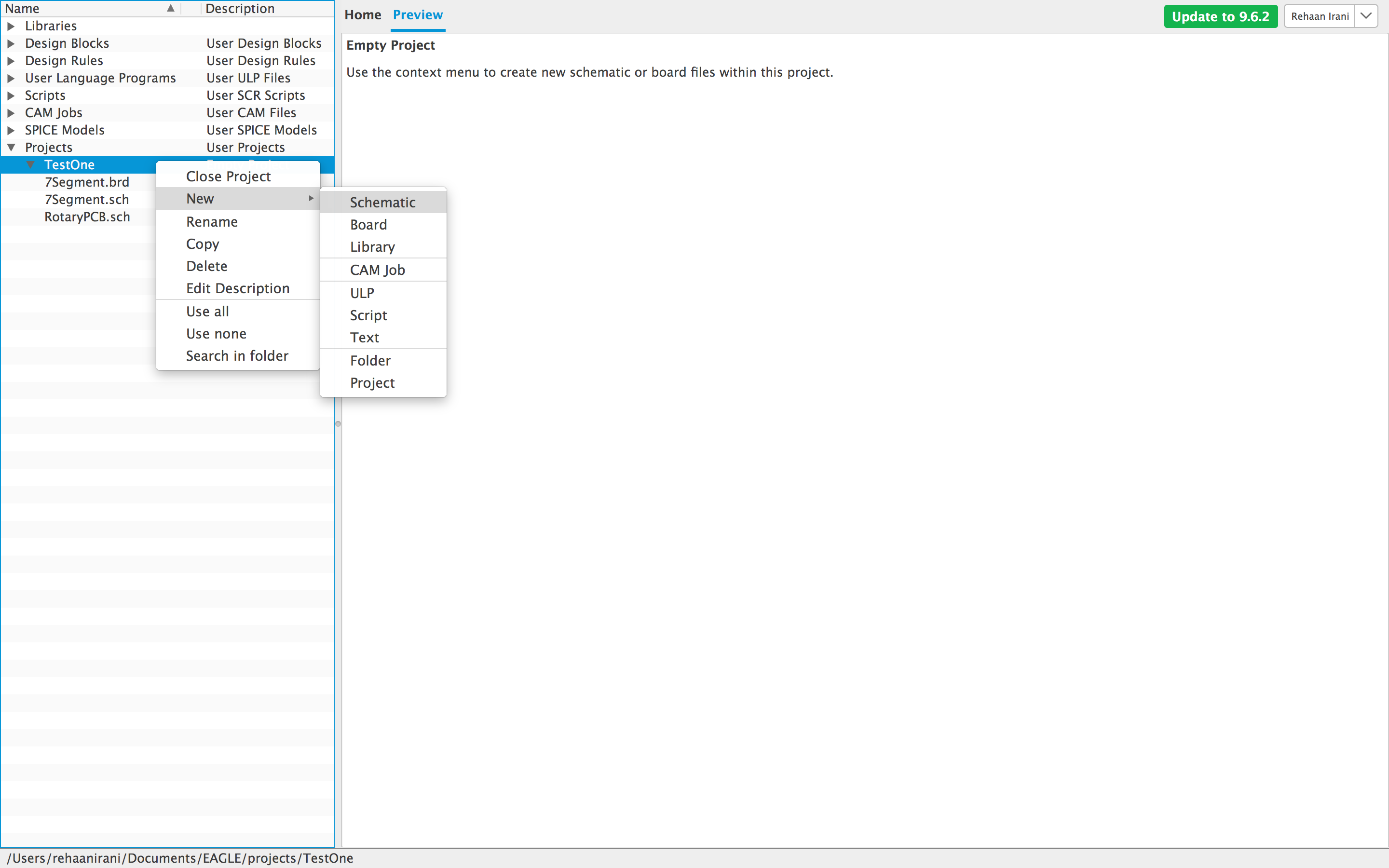
This step is relatively simple. All you are going to want to do is right-click on 'Projects' and select 'New Project'. I named my new project 'TestOne'. Once you have named it, go back under the projects tab and you should see your new project there.
In order to start making the schematic, right-click on your project, and click 'New', followed by 'Schematic'.
Add Parts & Configuration
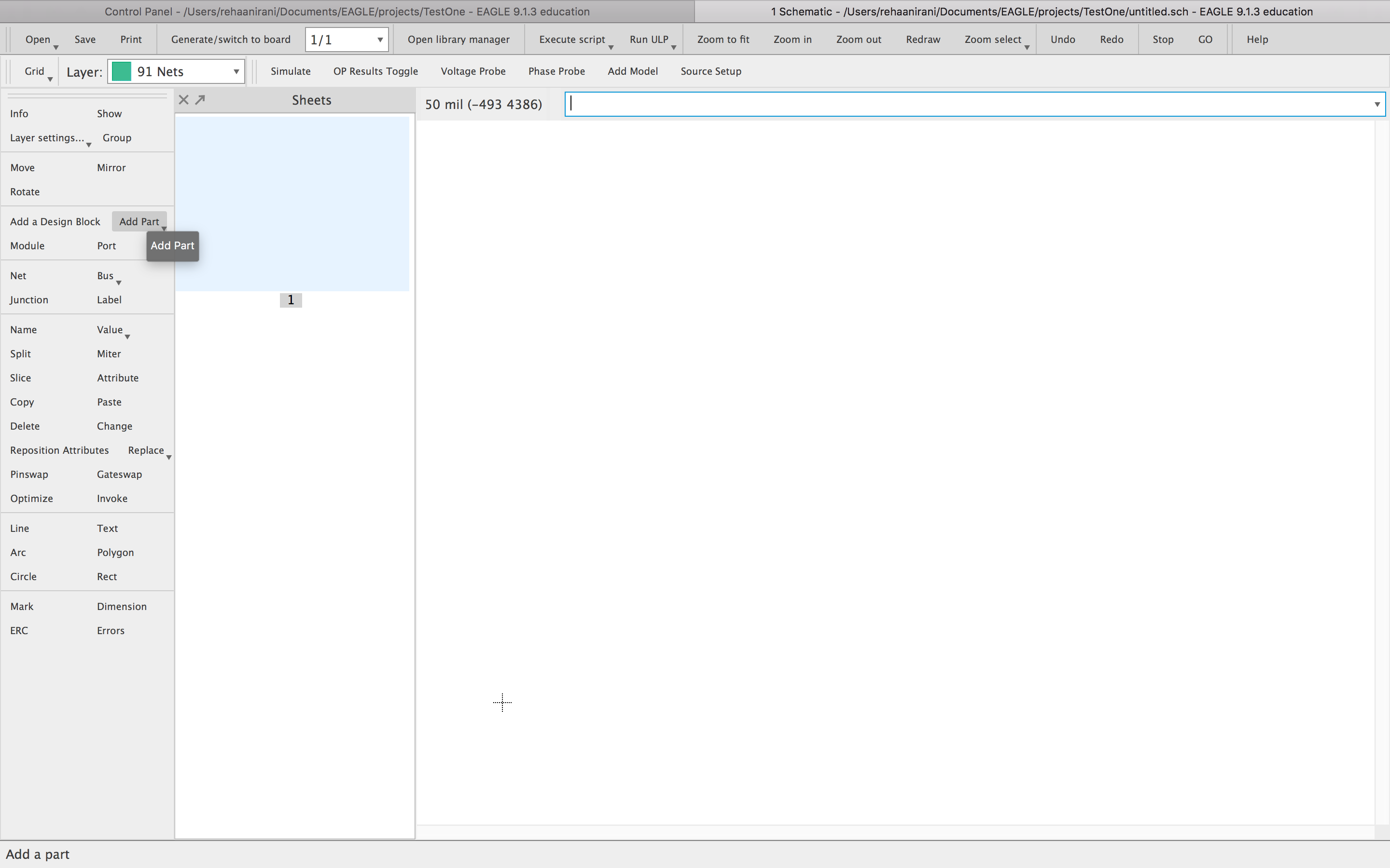
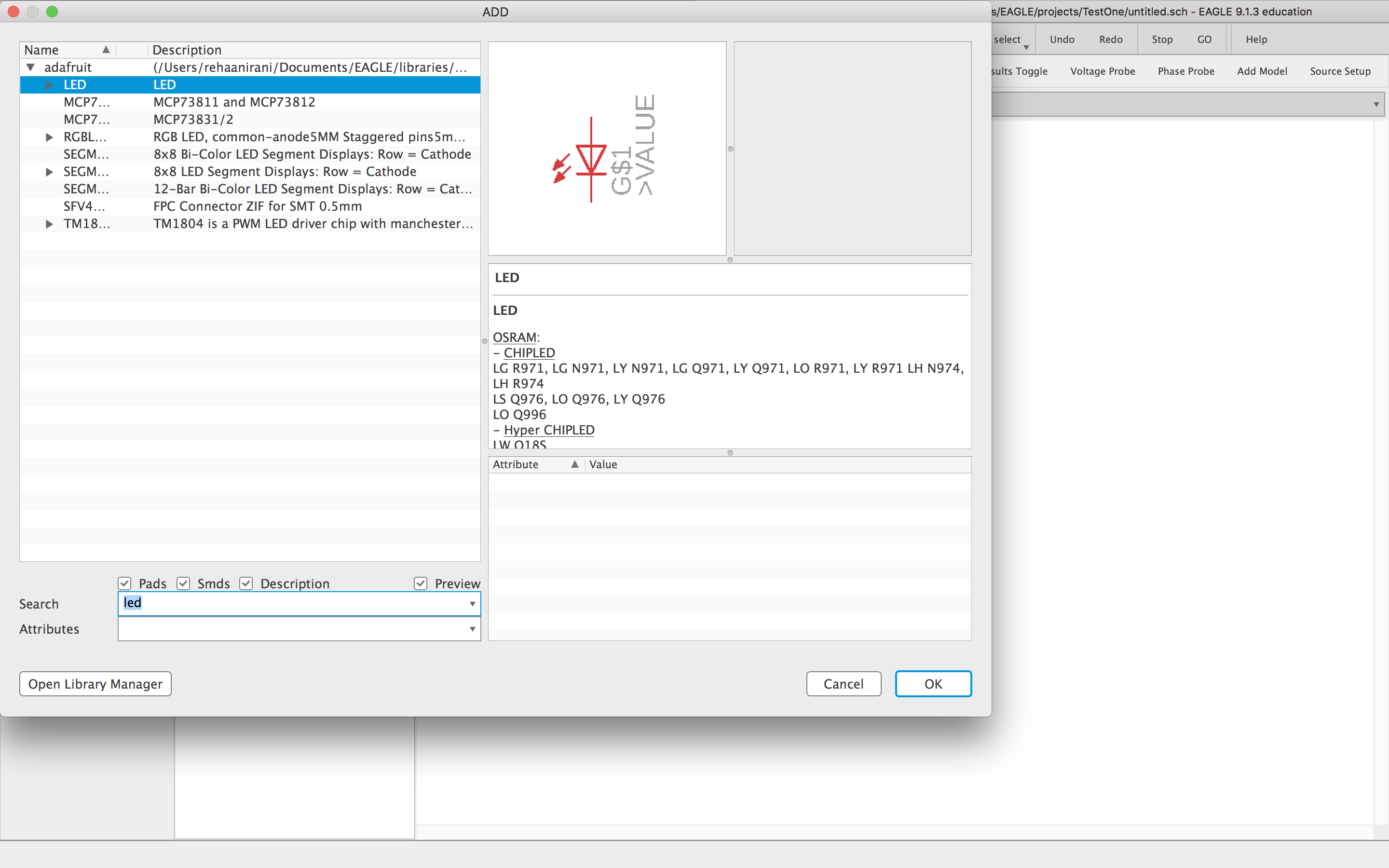
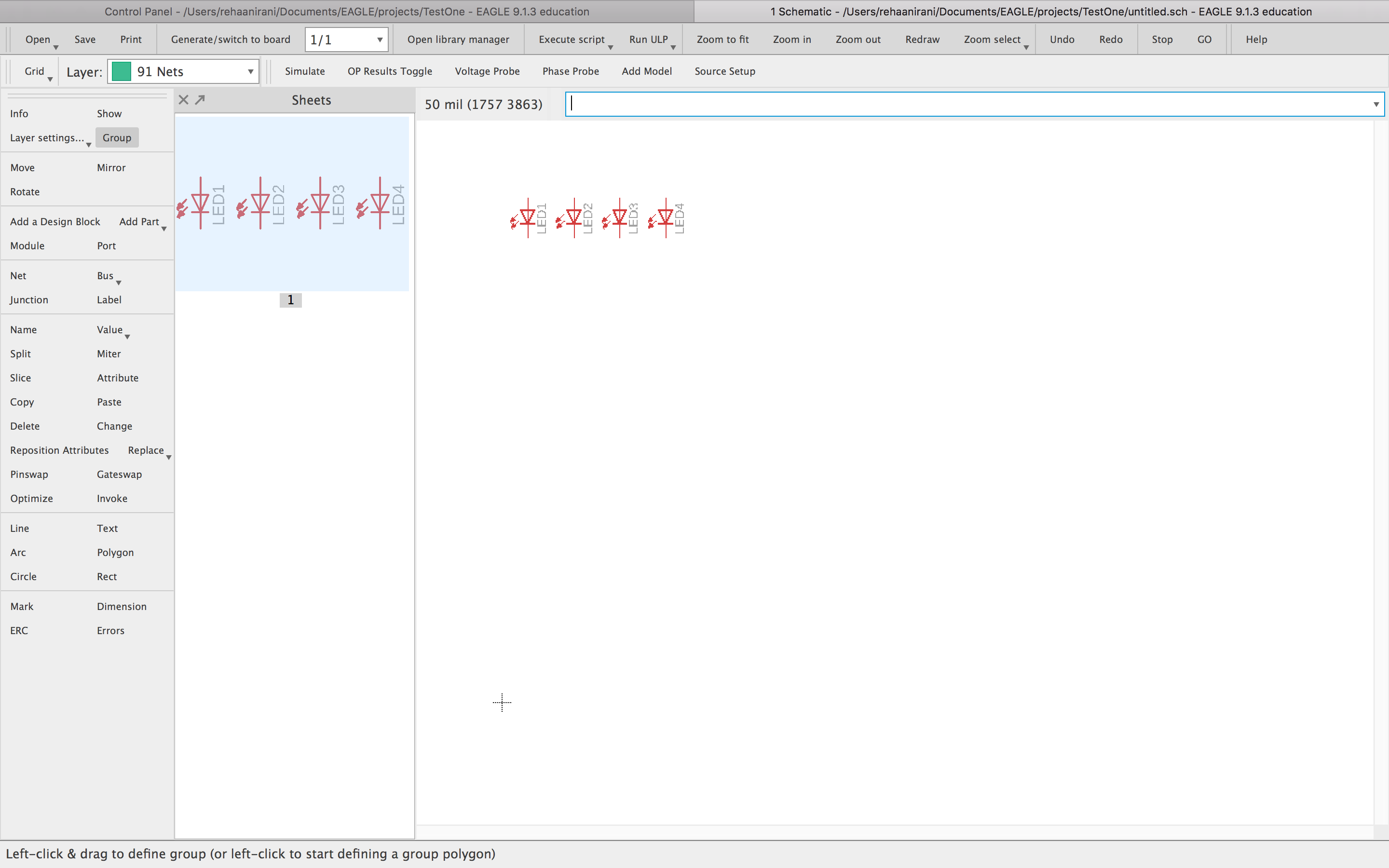
It is now finally time to put together the schematic! To do this, go ahead and select the 'add part' button on the left side of your screen as shown in the first photo.
You should be able to see all the parts from the Adafruit library here. To find a part, simply search for it and select it. It is important to remember that because this is a schematic that will be used to make a PCB, the parts you choose do not have to be EXACTLY what you are looking for. However, the shape, dimensions and number of holes have to match.
If you aren't able to find the required part, have a look at through other libraries posted on Autodesk's website or elsewhere on the web.
Finalise Schematic
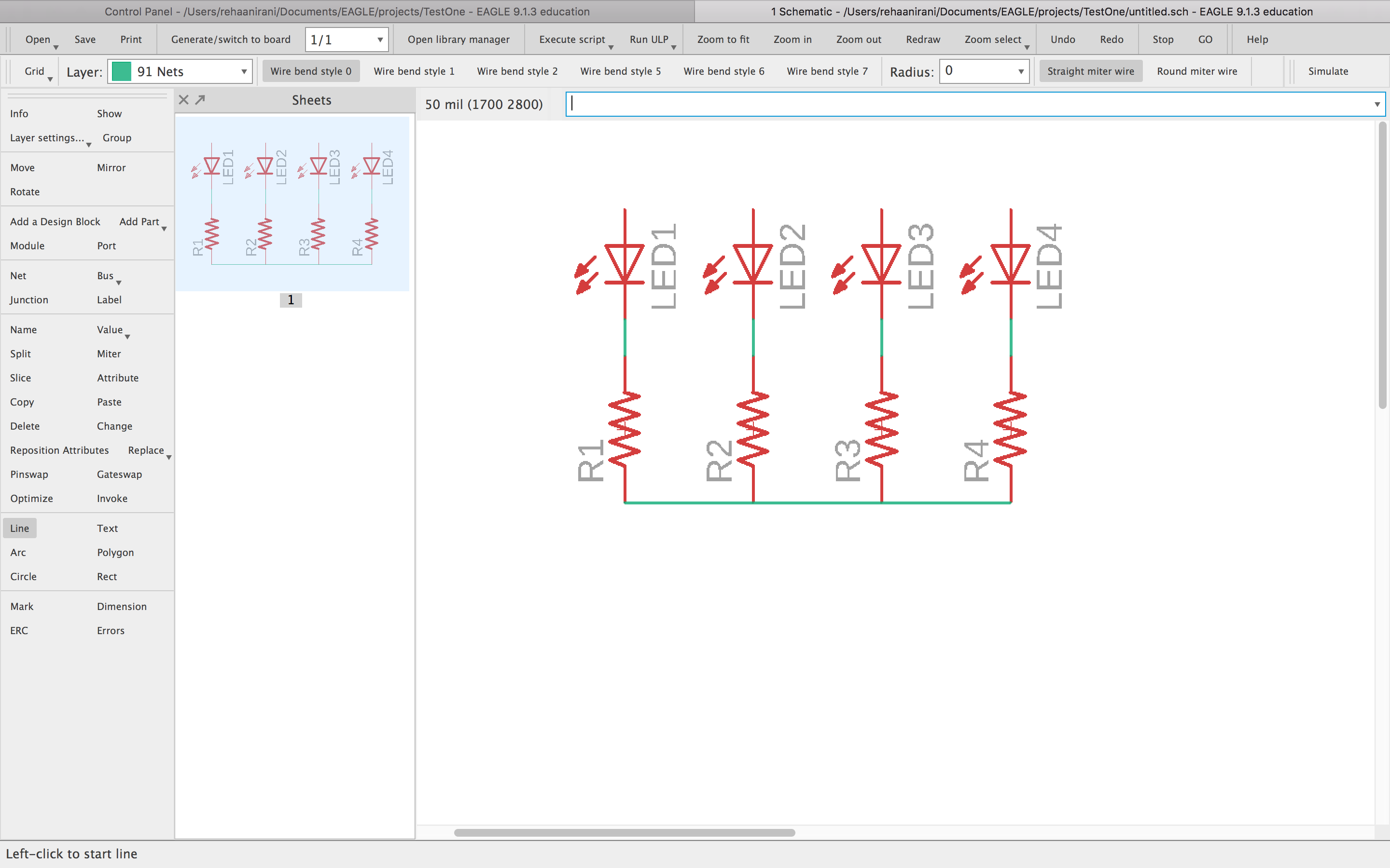
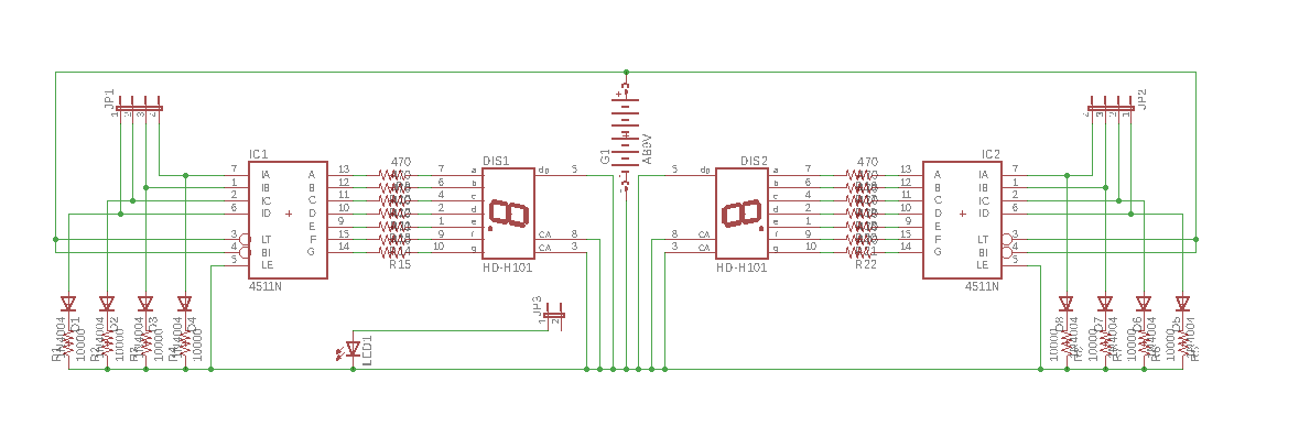
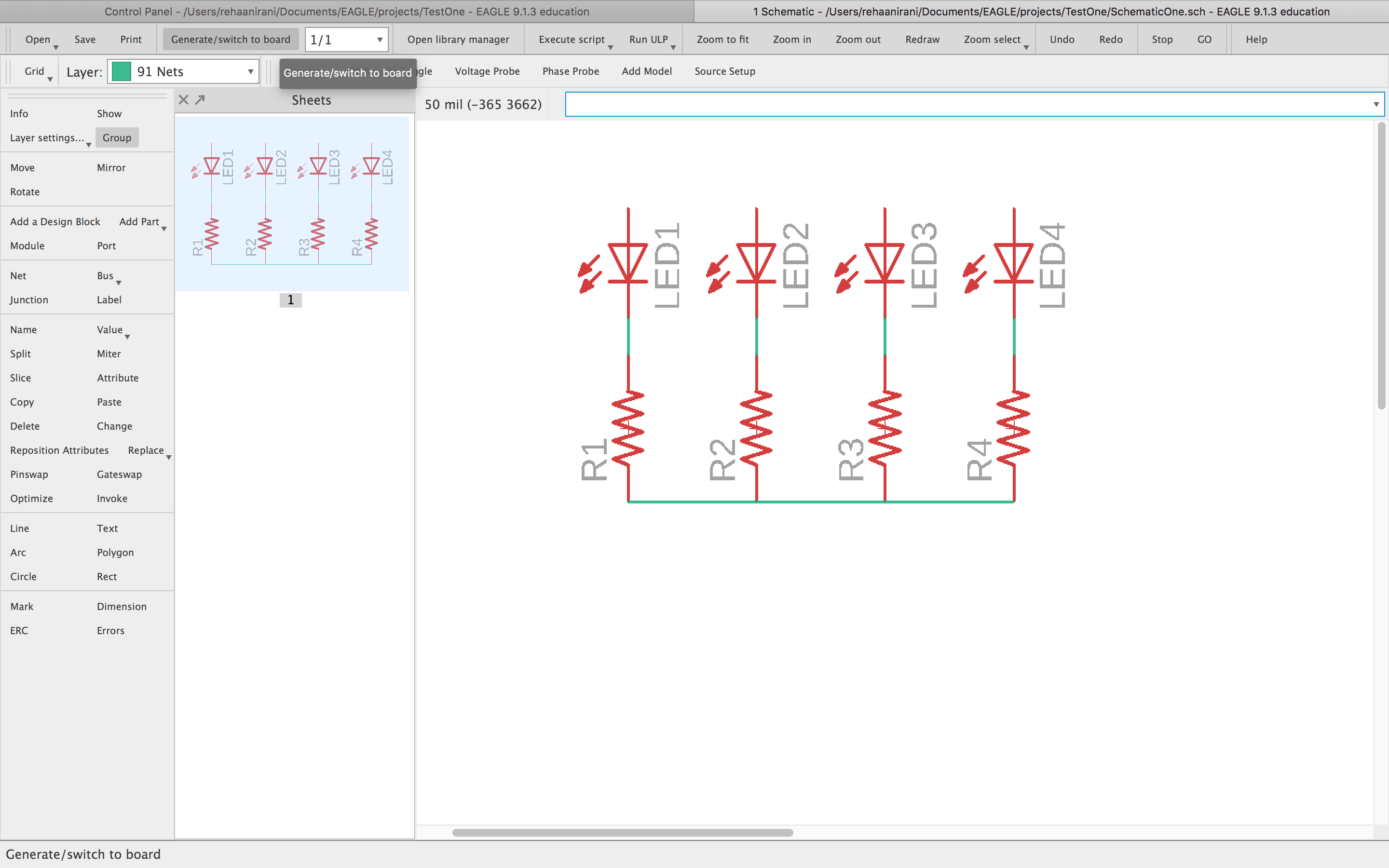
Once you have finished placing your parts on the screen, use the line tool on the left to make the necessary connections. Remember to save your work as well!
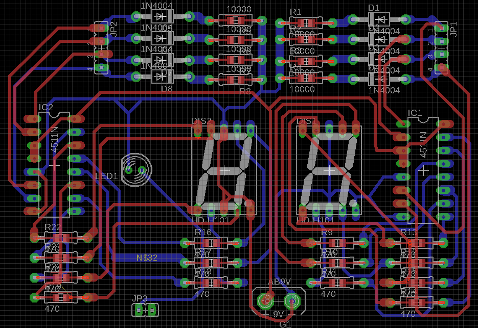
The photo on the top right is an example of what a more complex schematic could look like. This schematic was actually used to create the PCBs that I used in my Dice Generator project.
Now that you are happy with your schematic, it is time to convert it into a pcb board. This will enable you to start organizing the placements of each part. To do this, just go ahead a click 'generate/switch to board' on the top bar.
Layout
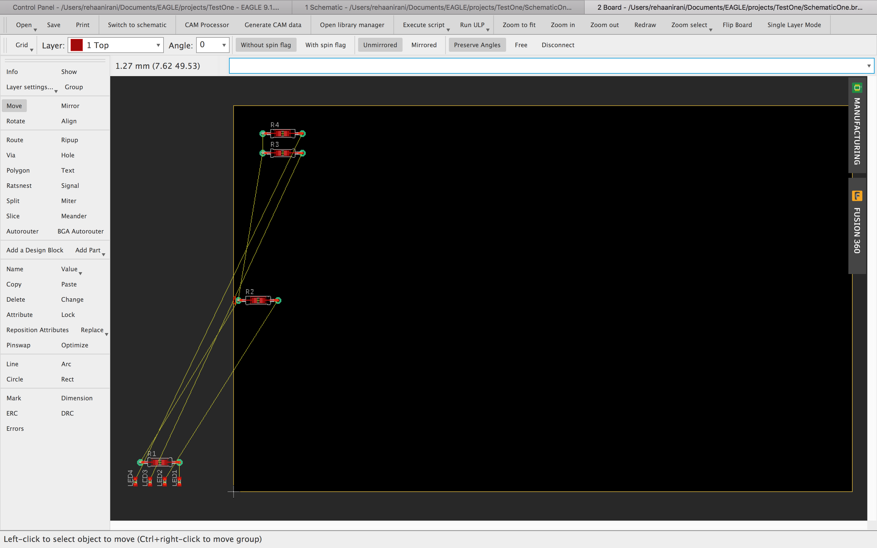
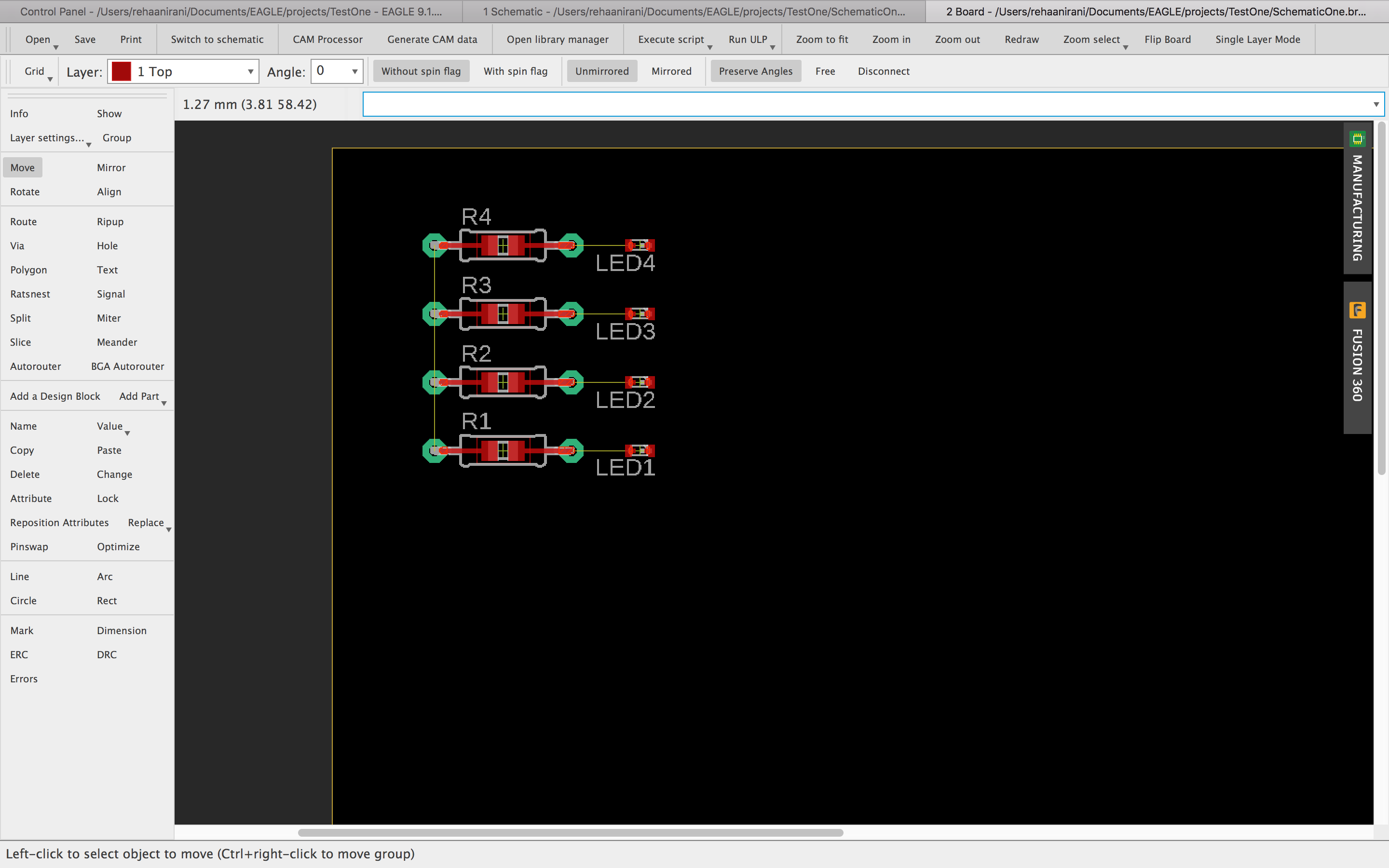
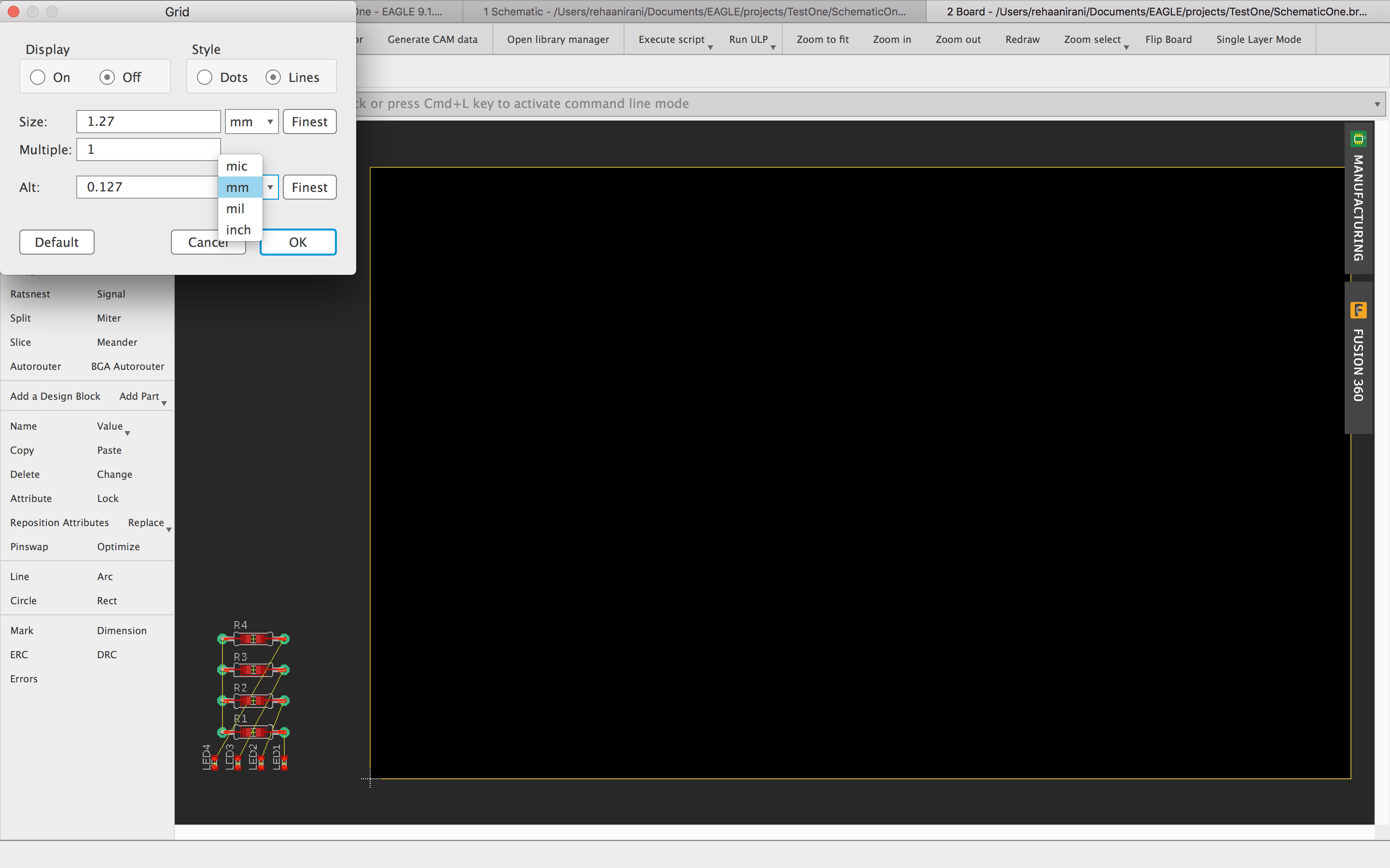
Organizing the placement of each component is crucial to the efficiency and size of each PCB. Remember that the larger your PCB, the more it will cost. Tracks between components should be as short as possible and as efficient as possible. If you are using a single-layered PCB, this is especially important as you cannot have tracks crossing over each other.
Read more about layered PCBs here.
PCB Design - Essentials + Routing
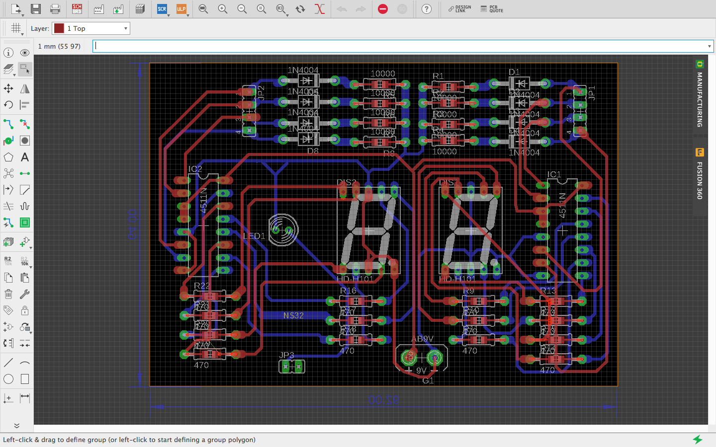
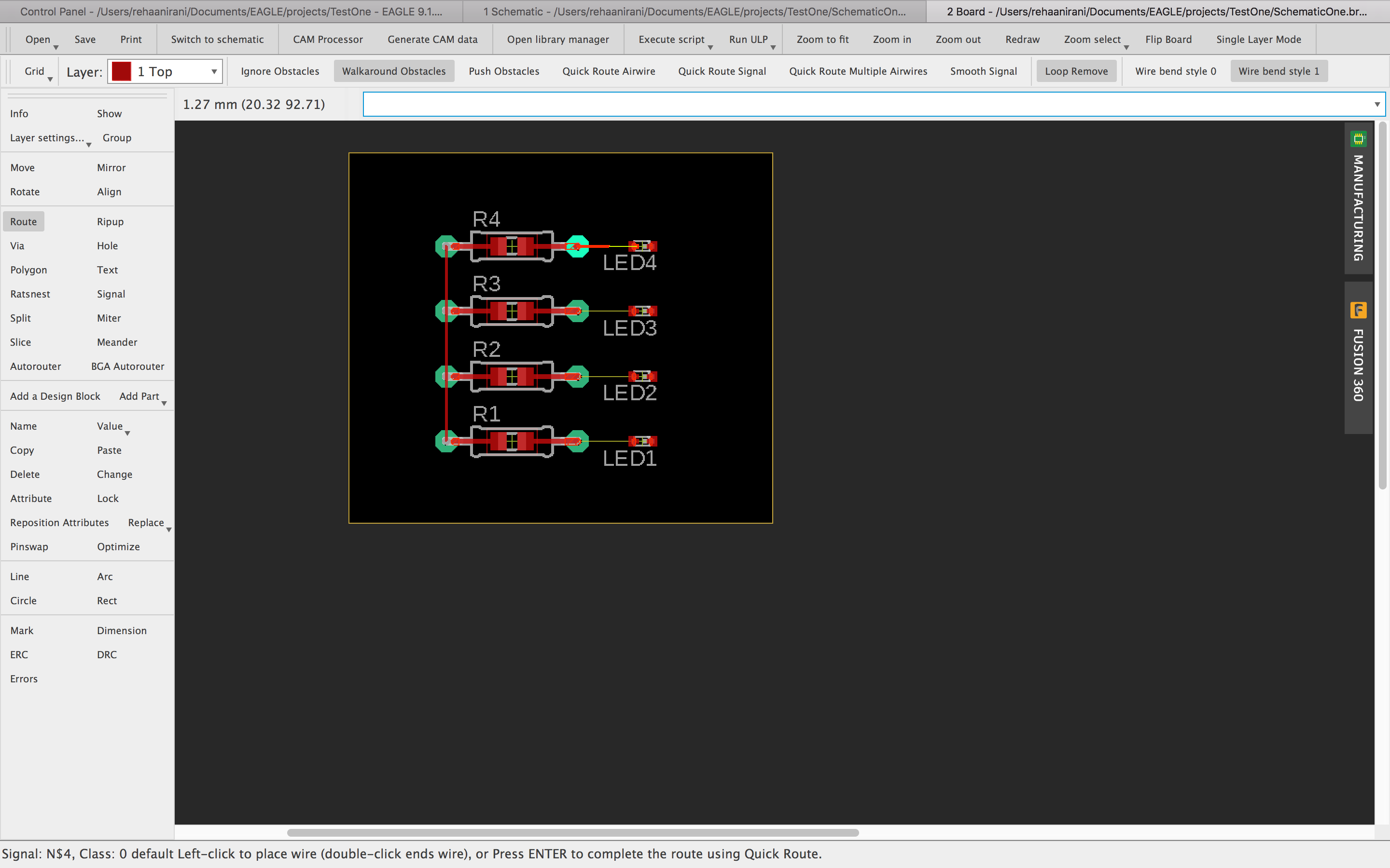
It is now time to route the PCB. The image above is an image of the fully routed PCB I created for the Dice Generator project. Routing can be done using the 'route' tool on the left control panel. If you are planning to route on more than one layer, you can interchange between these layers using the 'layer' drop-down menu above.
Before you start, here are some things to consider:
- None of the tracks should be at 90-degree angles. The maximum angle that should be allowed is 45 degrees. This is because sharp turns in tracks can affect the flow of current which may later cause errors in your circuit.
- The tracks must be of a minimum thickness depending on the current in order to avoid any errors in the circuit. This is because the thinner a track is, the more resistance is added to the track. Additionally, there is a higher likelihood of defects with thinner tracks.
- While the auto-router is a useful tool, do not place complete trust in it. Check each connection yourself and if necessary, do it manually.
- Watch the clearance between tracks. Make sure that they do not overlap and that they do not run too close to one another.
- Use reasonable pad sizes to ensure proper and strong solder joints.
A good article from ElectronicDesign - Link
Produce Gerber Files
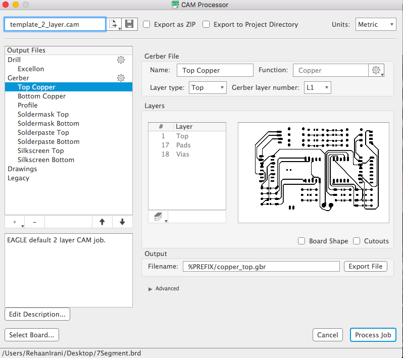
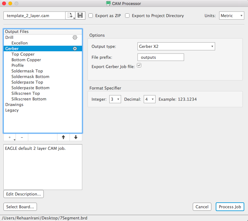
Now that the PCB is complete, it is time to convert it into a file type that overseas manufacturers will accept. To do this, we will be converting the PCB data into a Gerber file.
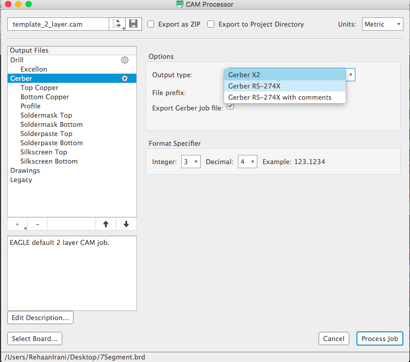
Proceed to find and click on 'CAM Processor', after which a window such as the one shown above should appear. In the list, find 'Gerber' and click on it. Under 'Output Type', you will most likely see Gerber X2. Change this to 'Gerber RS-274X' and then press process job.
Checking Gerber Files
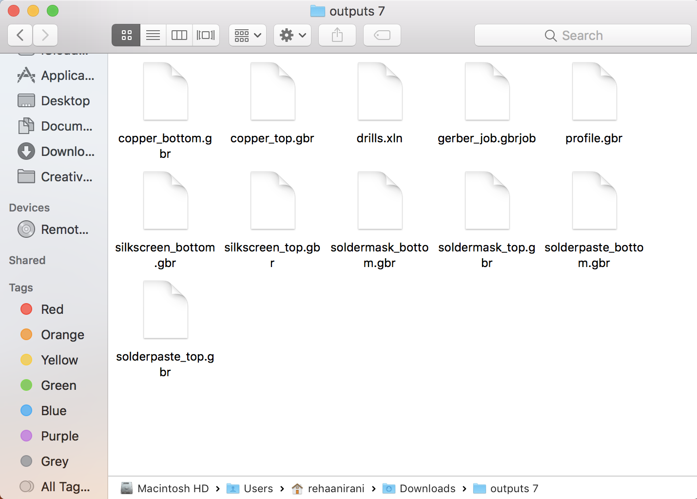
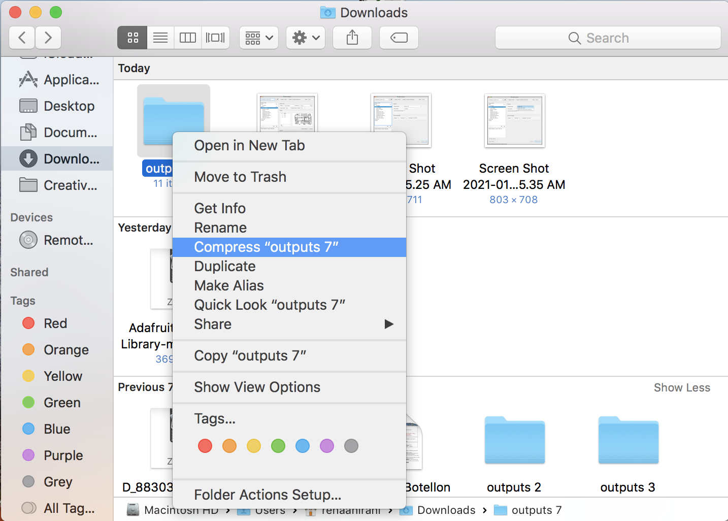
Once you press 'Process Job', a folder should be created containing your Gerber files. This will most probably be in your downloads folder. Once you find this folder, compress it into a ZIP file and it should be ready to go!
Finding a PCB Manufacturer

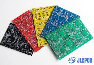
It is now time to pick a manufacturer (most are located in China). The two manufacturers that I have heard most about are SEEED and JLCPCB. When going through this process a while back, I ended up picking SEEED after I compared costs between the two platforms. The boards arrived on time and in excellent quality.
Both companies offer different deals for different types of PCBs. Be sure to explore both before making a decision!
Final Checks
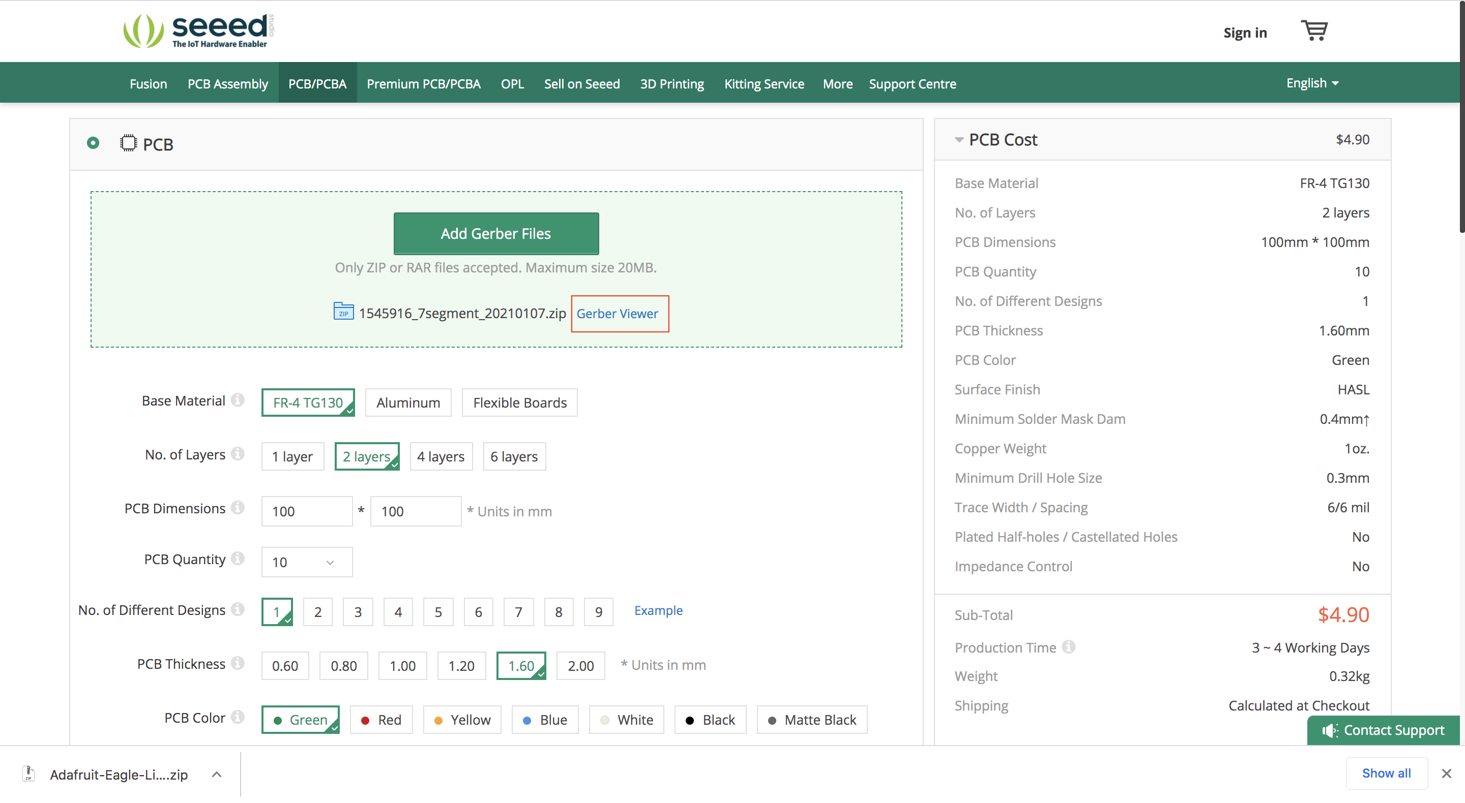
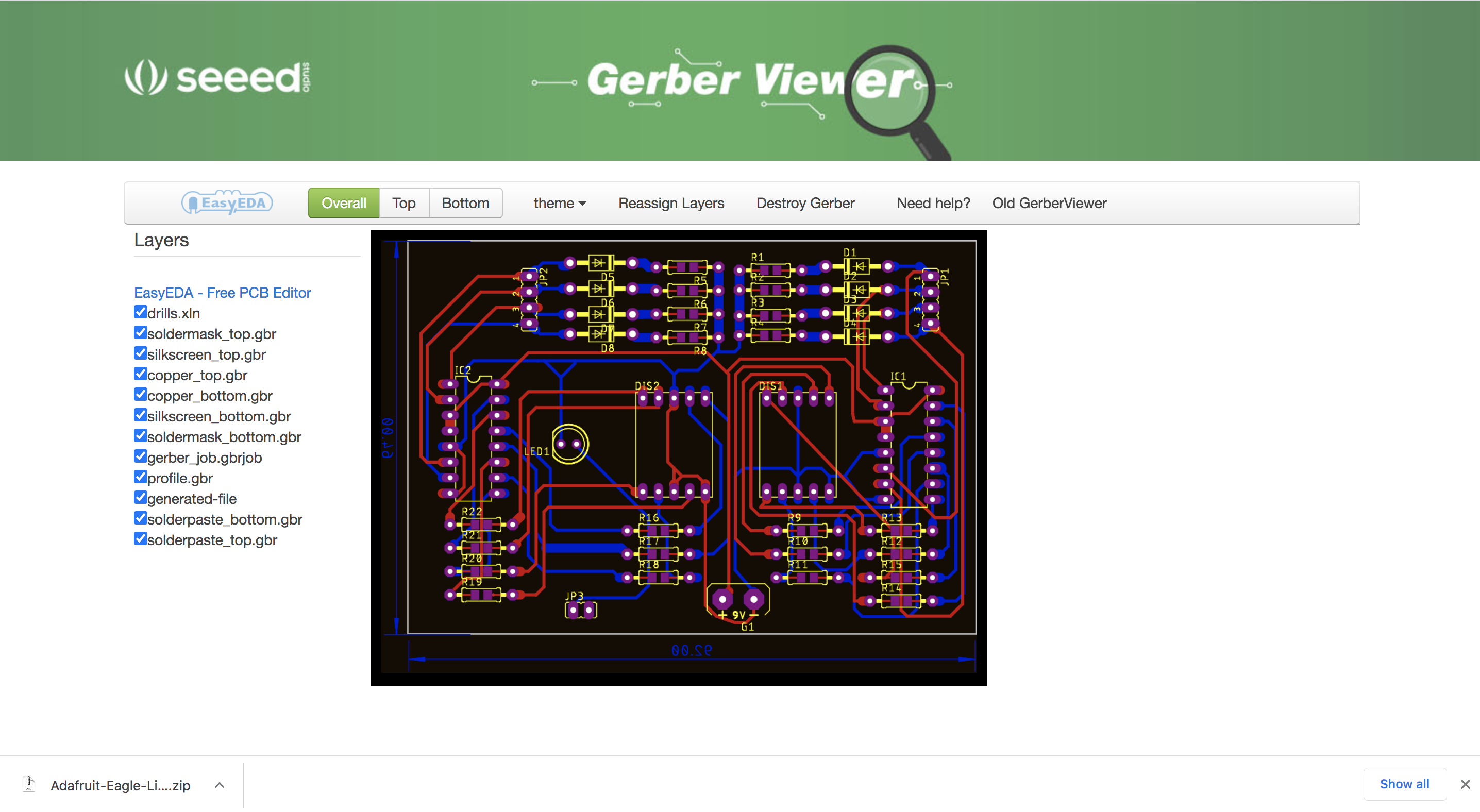
Whichever manufacturer you pick, there will be an option to preview your Gerber file before you place your order. Make sure you use this tool!!! This will allow you to see what the manufacturer will see in order to ensure everything is correct.
Order & Delivery - Final Result
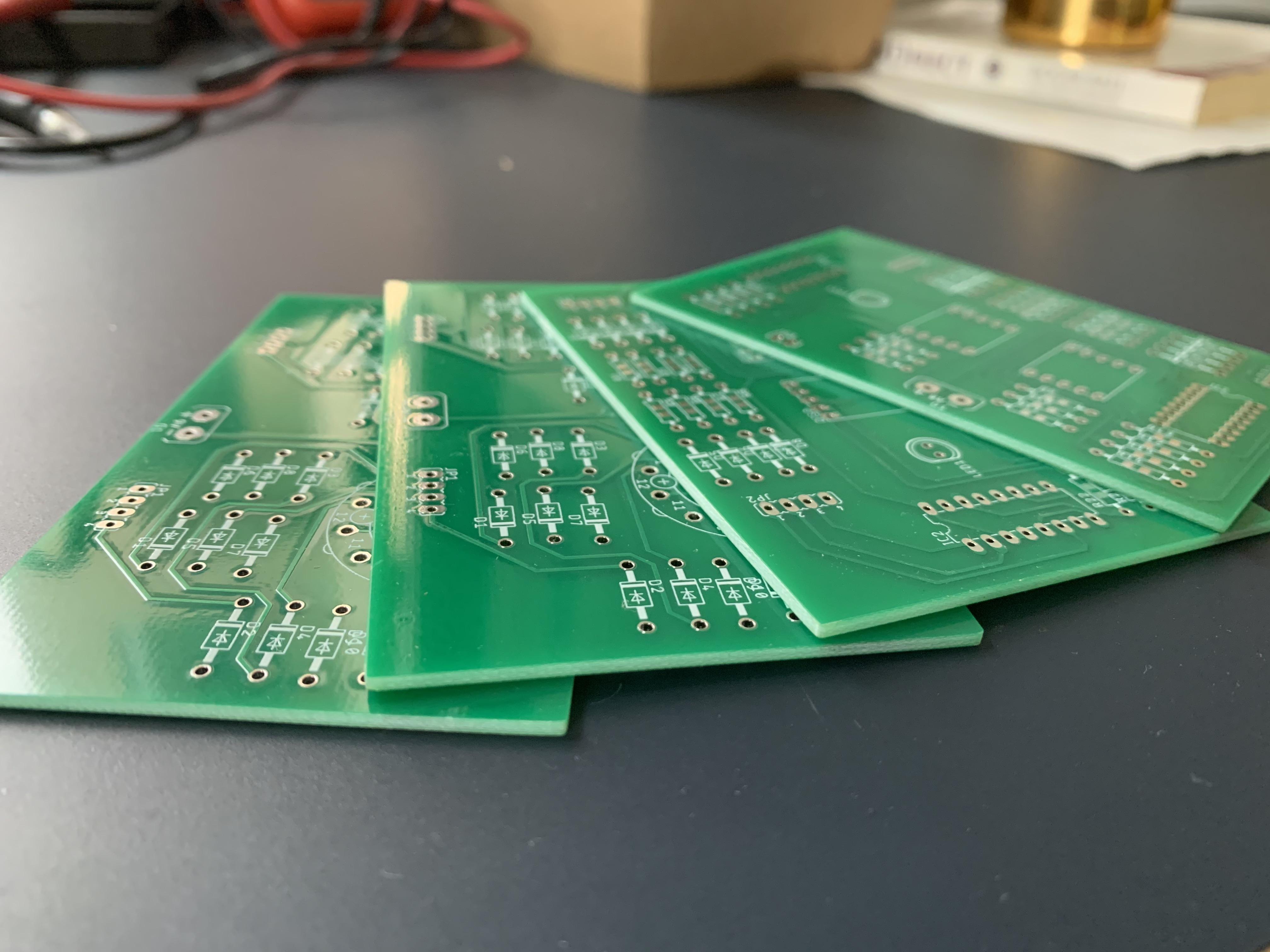
Now, just place your order, sit back, and relax :)
This instructable was quite brief and only included the very basics of Eagle. If you would like to learn more, check out Autodesk Eagle's latest introduction video - Link
Finally, if you have any questions, please don't hesitate to ask them in the comment section below!