At-tiny Test Using Arduino Ide
by hariramanil810 in Craft > Reuse
322 Views, 1 Favorites, 0 Comments
At-tiny Test Using Arduino Ide
.png)
.png)
.png)
If you have hard-time 3d printing stuff and other materials which i have provided in this project please refer the professionals for the help, JLCPCB is one of the best company from shenzhen china they provide, PCB manufacturing, PCBA and 3D printing services to people in need, they provide good quality products in all sectors
Please use the following link to register an account in JLCPCB
Pcb Manufacturing
----------
2 layers
4 layers
6 layers
PCBA Services
JLCPCB have 350k+ Components In-stock. You don’t have to worry about parts sourcing, this helps you to save time and hassle, also keeps your costs down.
Moreover, you can pre-order parts and hold the inventory at JLCPCB, giving you peace-of-mind that you won't run into any last minute part shortages. jlcpcb.com/RNA
3d printing
-------------------
SLA -- MJF --SLM -- FDM -- & SLS. easy order and fast shipping makes JLCPCB better companion among other manufactures try out JLCPCB 3D Printing servies
JLCPCB 3D Printing starts at $1 &Get $54 Coupons for new users
The high-performance, low-power Microchip 8-bit AVR® RISC-based microcontroller combines 8 KB ISP Flash memory, 512B EEPROM, 512B SRAM, six general purpose I/O lines, 32 general purpose working registers, one 8-bit timer/counter with compare modes, one 8-bit high-speed timer/counter, USI, internal and external Interrupts, 4-channel 10-bit A/D converter, programmable watchdog timer with internal oscillator, three software selectable power saving modes, and debugWIRE for on-chip debugging. The device achieves a throughput of 20 MIPS at 20 MHz and operates between 2.7-5.5 volts.
By executing powerful instructions in a single clock cycle, the device achieves throughputs approaching one MIPS per MHz, balancing power consumption and processing speed.
Supplies
.png)
.png)
.png)
The ATtiny85 is a microcontroller in a similar vein to the but with much less IO pins, smaller memory and a smaller form factor. In fact, when we talk about the ATtiny85 we refer to the IC itself rather than the board. The ATtiny85 can be used as a bare chip on a breadboard, as long as you can supply the correct power for the device.
Despite the small package, the ATtiny85 comes with a remarkable number of ways in which we can interface. At the most basic level, we have 5V logic digital I/O pins, three of which can also be used as analog pins for use with components such as the TMP36 sensor. Four of the available pins can also be used with Pulse Width Modulation (PWM). Also available is I2C and SPI for use with other types of sensors and devices.
Introduction
.png)
.png)
As per the datasheet, it has 8 KB of flash, an 8-MHz internal RC oscillator that can be used as the default clock & 512 bytes of EEPROM and SRAM.
In achieving a throughput of 20 MIPS, it takes 20 MHz and operates between 2.7-5.5V.
It also has two 8-bit timers or counters, one high-speed, with four pulse-width modulations (PWM) outputs, and a four-channel 10-bit ADC.
An ADC converter with a 10 bit & programmable watchdog timer is added to the device which makes it suitable for resetting the device in case it gets stuck in an infinite loop and sensor interfacing.
Although it consists of 8 pins only, it can perform almost every function that a simple microcontroller can do. We will get a better idea of its functionality in the pinout specification.
What does the number 85 in ATtiny85 represents?
In the ATtiny series, the first digit that comes after ATtiny represents the flash memory in kibibyte (KiB). Thus, an ATtiny85 consists of 8KiB flash memory.
The second digit represents the model type. You can expect more powerful and newer models to have higher numbers. Here you can see that ATtiny85 is a 2005 model.
Editing
.png)
.png)
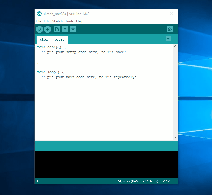
Installing the software
We shall be using the Arduino IDE to write the code for this project. So if not already installed, download a copy from the Arduino website and install.
Open the Arduino application and click on File >> Preferences and past the following into the Additional Boards Managers URLs: dialog.
http://digistump.com/package_digistump_index.json
Next, go to Tools >> Board >> Boards Manager and from the drop-down menu select “Contributed”.
Select the “Digistump AVR Boards” and click Install.
The install process will take some time, but once completed the installation should trigger an auto install of the drivers for the board.
If the driver install fails to run after adding the board to your list, open the command prompt and enter the following command. Remember to change the USERNAME to match your own!
C:\Users\**YOUR USERNAME**\AppData\Local\Arduino15\packages\digistump\tools\micronucleus\2.0a4\post_install.bat
This will install the drivers for the ATtiny85, and there may be a red cross in the post install screen, but we can confirm that the instal is correct.
To use the ATtiny85 in the Arduino IDE we need to set it as our board.
Go to Tools >> Board >> and select Digispark (Default - 16.5MHz) don’t worry about the Port.
Building the circuit
On the breadboard, build the circuit as shown in the diagram. The LED cathode (-) legs are on the left of the image, and they connect to a single ground pin on the ATtiny85 via a 330 Ohm resistor. The male to male jumper jerky connects the 330 Ohm resistors for two of the LEDs to the third, creating a single Ground connection that is connected to the ATtiny85. The anode (+) leg of the LED is connected directly to Pins 0,1,2 using the male to female jumper jerky.
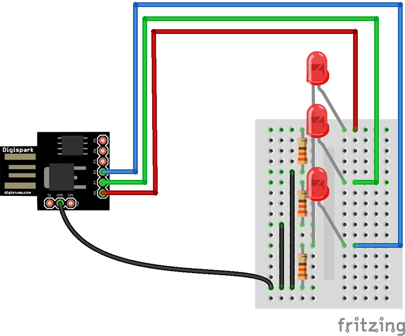
Don’t insert the ATTiny85 just yet. First, we need to write some code.
In the Arduino IDE, we shall set up the three pins (0,1,2) that will be used as outputs first and will flash the LEDs attached to them.
Coding
.png)
.png)
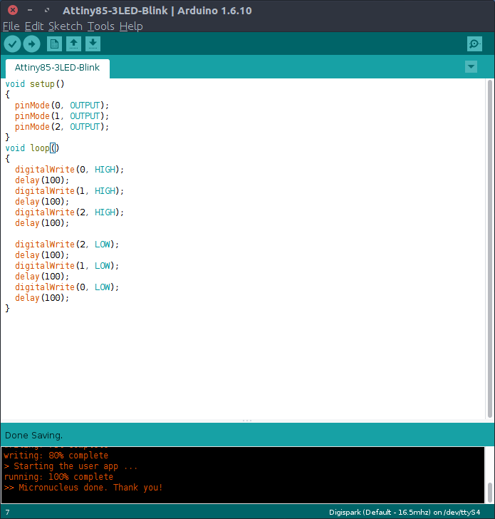
Now for the code that will continually loop round, creating the effect of cycling through the LEDs. We start by turning on each LED (HIGH) and then using a delay of 1/10 of a second between each LED turning on.
void loop()

{

  digitalWrite(0, HIGH);

  delay(100);

  digitalWrite(1, HIGH);

  delay(100);

  digitalWrite(2, HIGH);

  delay(100);
Still inside of the loop, we now need to turn off the LEDs in reverse order by pulling the output LOW for each LED. We also keep the same delay between LEDs to create a rhythmic looping pattern.
  digitalWrite(2, LOW);

  delay(100);

  digitalWrite(1, LOW);

  delay(100);

  digitalWrite(0, LOW);

  delay(100);

}
Flashing the code
To write the code to our ATTiny85 click on Sketch >> Upload or click on the right-hand arrow. In the output window, at the bottom of the Arduino IDE, you will be prompted to insert the ATtiny85, do this and the code will be flashed to the ATtiny85 within a few seconds. Your LEDs will now start flashing in a cycling pattern.
Renistalling
.png)
.png)
Notes
- ↑ timers x waveform generators
- ↑ timer0 can use clocks up to the core clock, timer1 can use clocks up to 64MHz
- ↑ 4 pins are usable, but only 3 unique generators can be attached. The 4th pin would be the inverse of OC1B on the 3rd pin.
- ↑ Inverted outputs with configured dead zones can be set up for the 64MHz-capable timer1.
- ↑ timer/counter1 is a 10-bit counter that can use clocks to 64MHz.
- ↑ The PWM channels are based on the 10 bit counter with a maximum of 64MHz clock. Each PWM channel can generate two outputs, normal and inverted, on distinct IO pins. Each pair of outputs can be configured to have a dead-time between their on-states.
- ↑ ADC only on ATtiny5/10, and channels are 8 bits instead of 10
- Package column - the number after the dash is the number of pins on the package. DIP packages in this table are 0.3 inches (7.62 mm) row-to-row. SOwww means SOIC package with a case width of 'www' in thousandth of an inch. Though some package types are known by more than one name, a common name was chosen to it easier to compare packages.
- UART/I²C/SPI columns - green cell means a dedicated peripheral, * yellow cell means a multi-feature peripheral that is chosen by setting configuration bits. Most USART peripherals support a minimum choice between UART or SPI, where as some might support additional choices, such as LIN, IrDA, RS-485.
- Timers column - recent families add a 12-bit timer, plus a 16-bit Real Time Counter (RTC) that is driven by a 32.768KHz clock (feature designated with 'R' in the table).
- ADC chans column - the total number of analog channels that are multiplex into the ADC input. Most parts have one ADC, a few have two ADC.
- Pgm/Dbg column - flash programming and debugging protocols: HVPP means High Voltage Parallel Programming 12V protocol, HVSP means High Voltage Serial Programming 12V protocol, ISP means In-System Programmable protocol, uses SPI to program the internal flash. TPI is Tiny Programming Interface. dW means debugWIRE protocol. UPDI means Unified Program and Debug Interface protocol (newest)
Abbreviations
- TWI: Many of Atmels microcontrollers contain built-in support for interfacing to a two-wire bus, called Two-Wire Interface. This is essentially the same thing as the I²C interface by Philips, but that term is avoided in Atmel's documentation due to trademark issues.
- USI: Universal Serial Interface (not to be confused with USB). The USI is a multi-purpose hardware communication module. With appropriate software support, it can be used to implement an SPI, interface. USART peripherals have more features than USI peripherals.
Installing
.png)
.png)
As per the datasheet, it has 8 KB of flash, an 8-MHz internal RC oscillator that can be used as the default clock & 512 bytes of EEPROM and SRAM.
In achieving a throughput of 20 MIPS, it takes 20 MHz and operates between 2.7-5.5V.
It also has two 8-bit timers or counters, one high-speed, with four pulse-width modulations (PWM) outputs, and a four-channel 10-bit ADC.
An ADC converter with a 10 bit & programmable watchdog timer is added to the device which makes it suitable for resetting the device in case it gets stuck in an infinite loop and sensor interfacing.
Although it consists of 8 pins only, it can perform almost every function that a simple microcontroller can do. We will get a better idea of its functionality in the pinout specification.
What does the number 85 in ATtiny85 represents?
In the ATtiny series, the first digit that comes after ATtiny represents the flash memory in kibibyte (KiB). Thus, an ATtiny85 consists of 8KiB flash memory.
The second digit represents the model type. You can expect more powerful and newer models to have higher numbers. Here you can see that ATtiny85 is a 2005 model.
The serial peripheral interface (SPI) is used for communicating microcontrollers with other peripheral devices like sensors, SD cards, etc.
It consists of a separate clock and data lines with the addition of a select line to choose the required device to build communication. This allows both connected devices to layout the same communication path following one communication protocol.
I2C Communication
I2C protocol is a 2-wire protocol, incorporated in the device to connect low-speed devices like DAC converters & ADC, I/O interfaces & microcontrollers.
Serial Data (SDA) & Serial Clock (SCL) are the two wires and are the main part of this communication protocol.
Brown Out Reset (BOD)
This function helps reset the controller once Vdd (voltage supply) comes below a brownout threshold voltage. The multiple voltage ranges are provided once the power drops below the voltage supply line.
Interrupt
This function works on a priority basis. It puts the main function on hold and executes the required instructions that are necessary at that time. Once it is executed, the executing code puts the controller again to the main program.
ADC
In this device, the ADC module is a valuable feature that helps to make it more compatible with the sensors. It is a 10-bit module that consists of 4 channels which are lesser than the number of modules introduced by Microchip (7 or 12 channels).
Result
.png)
The ATtiny85 pinout is discussed below:
Pin 1 (PB5)- It is for an analog pin ADC0 and is used for analog sensors.
Pin2 (PB3)- It is for an analog pin ADC3 and also for crystal oscillator XTAL1.
Pin3 (PB4)- It is for analog pin ADC2 and also used for crystal oscillator XTAL2.
Pin4 (GND)- It should be connected to the Ground.
Pin5 (PB0)- This pin is used as MOSI (Master Out Slave In). It can be used as a master line for sending data to the peripherals for SPI communication and SDA for I2C Communication.
Pin6 (PB1)- This pin is used as MISO(Master In Slave Out). It can be used as a Slave line for sending data to the master.
Pin 7 (PB2)- This can be used as SCK for SPI Communication and SCL for I2C Communication.
Pin 8 (Vcc)- It is used as Vcc Pin & 5V is applied on it.
Detailed description of the pins
Power
ATtiny85 has two power pins. One is used for the power supply while the other connects to the ground. The power supply to the ATtiny must not exceed the rated voltage.
Pin8– Vcc
Pin4-GND
Oscillator/Clock
Attiny85 has an 8MHz internal clock and its clock value varies from 0-8MHz. But it can expand its oscillator up to 20MHz. So, to increase the oscillator value, it should be connected to the oscillator pins.
GPIO2– XTAL1/CLKI
GPIO3-XTAL2/CLKO
Digital input/output
In ATtiny85, any pin can be used for input and output signal but, it should be mentioned in the program before. These pins are used as bidirectional Input/Output. Except for the power supply pin, any pin we can use for Input/Output purposes.
GPIO5- PB0
GPIO6- PB1
GPIO7- PB2
GPIO2- PB3
GPIO3- PB4
GPIO1- PB5
Interrupt
ATtiny85 has one interrupt pin. This pin can be controlled by any sensor output, or manually via a button.
GPIO7- INT0
SPI
The SPI pins on Attiny85 are:
GPIO5- MOSI
GPIO6-MISO
GPIO7- SCK
GPIO1- Debugging wire(DW)
- MOSI is used to send the data
- MISO is used for receiving the data
- SCK for the clock
- DW for programming
I2C
The I2C communication protocol is also available in Attiny85. In this protocol, data is sent and received by a single line while another line sends a clock pulse through which data is kept in sync by the time. The I2C pins are:
GPIO5- SDA(Data)
GPIO7- SCL(Clock)
Timer
ATtiny85 consists of two timers, i.e., Timer 0 and Timer 1, that are used to count the clock pulses. These two clocks work according to the internal clock, but the Timer 0 can be operated by an external clock pulse.
These both Timers consist of 8 bit. The Timers pins are:
GPIO7-Timer 0
Counter/Timer and PWM
PWM stands for Pulse Width Modulation. The Attiny85 consists of four PWM channels.
In Attiny85, there are some special pins and with the combinations of the internal PWM signal input, it can be used to drive the external power efficiently.
These pins function according to a particular time which is known as Dead Time Generator. The timer counts the value and compares its value until it reaches zero.
In ATtiny85, Timer 0 and Timer1 are used to count two dead generator values and the output signal comes in the non-overlapping form.
GPIO-OC1B
GPIO-OC1B’
GPIO-OC0B
GPIO-OC0A
GPIO-OC1A
GPIO-OC1A’
Analog Comparator
Attiny85 has an internal analog comparator through which an analog signal can be compared in the form of inverted and non–inverted. Within the register, the output which comes from the comparison is stored and can be used for further purposes. Analog comparator pins that are available in Attiny85:
The chip has two timers that help in generating a delay in the running process of certain functions when they perform in timer mode. The timer mode increases the instruction cycle.
While in the counter mode, these timers are used to count the number of intervals on a specific function inside the controller. The counter mode is used to increase the rising and falling edge of the pin in it.