A Guide to Artistic PCB's
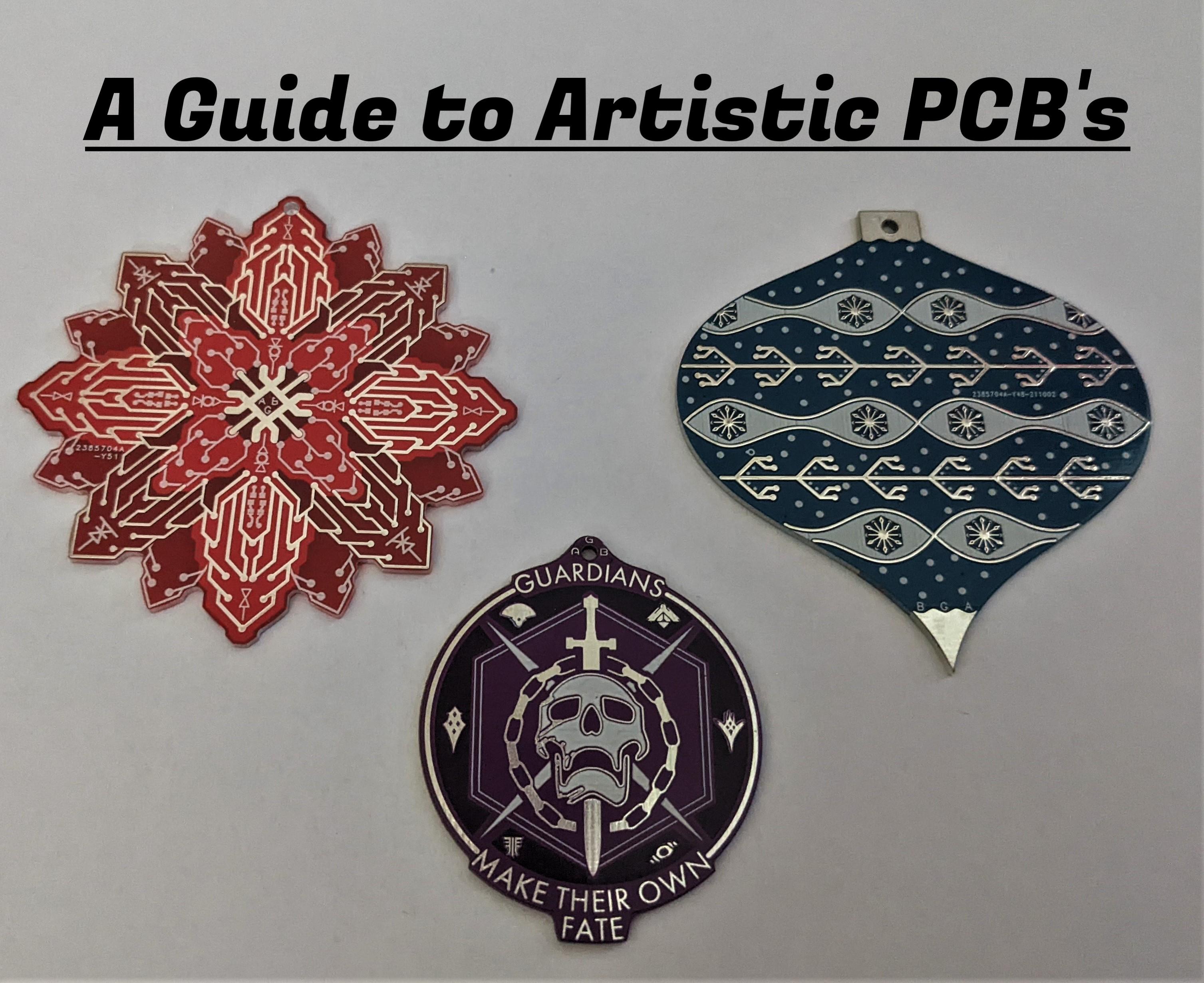
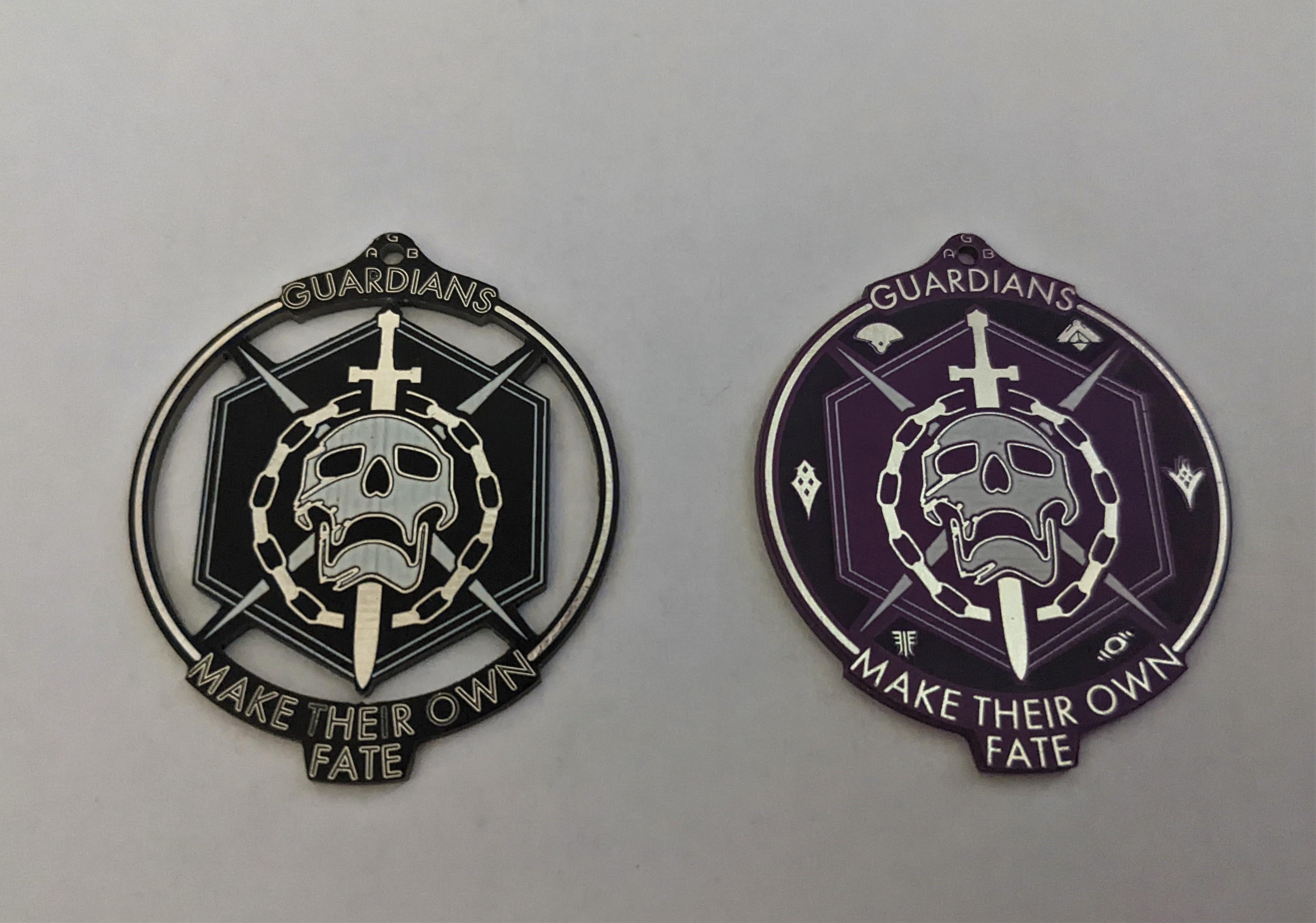
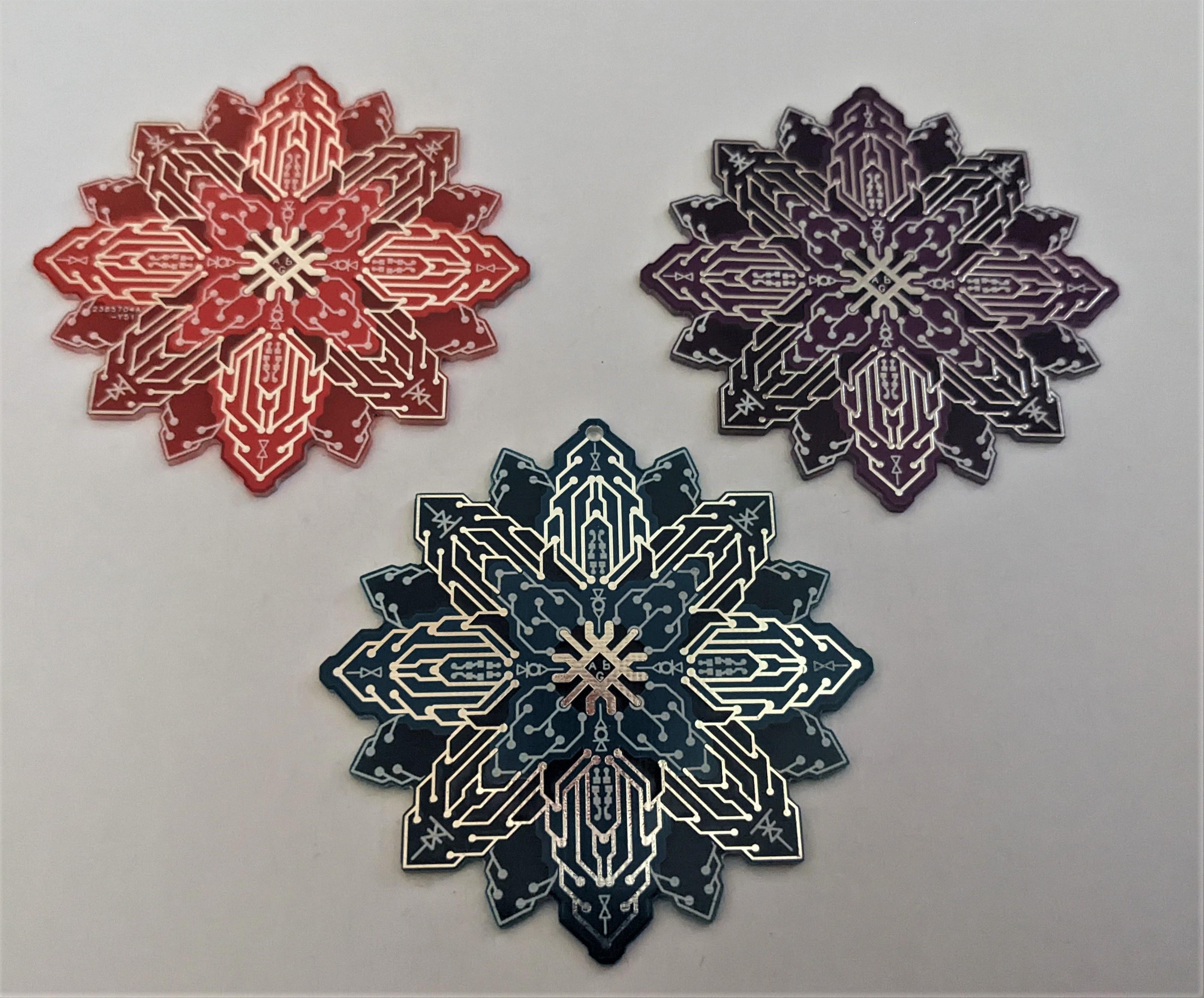
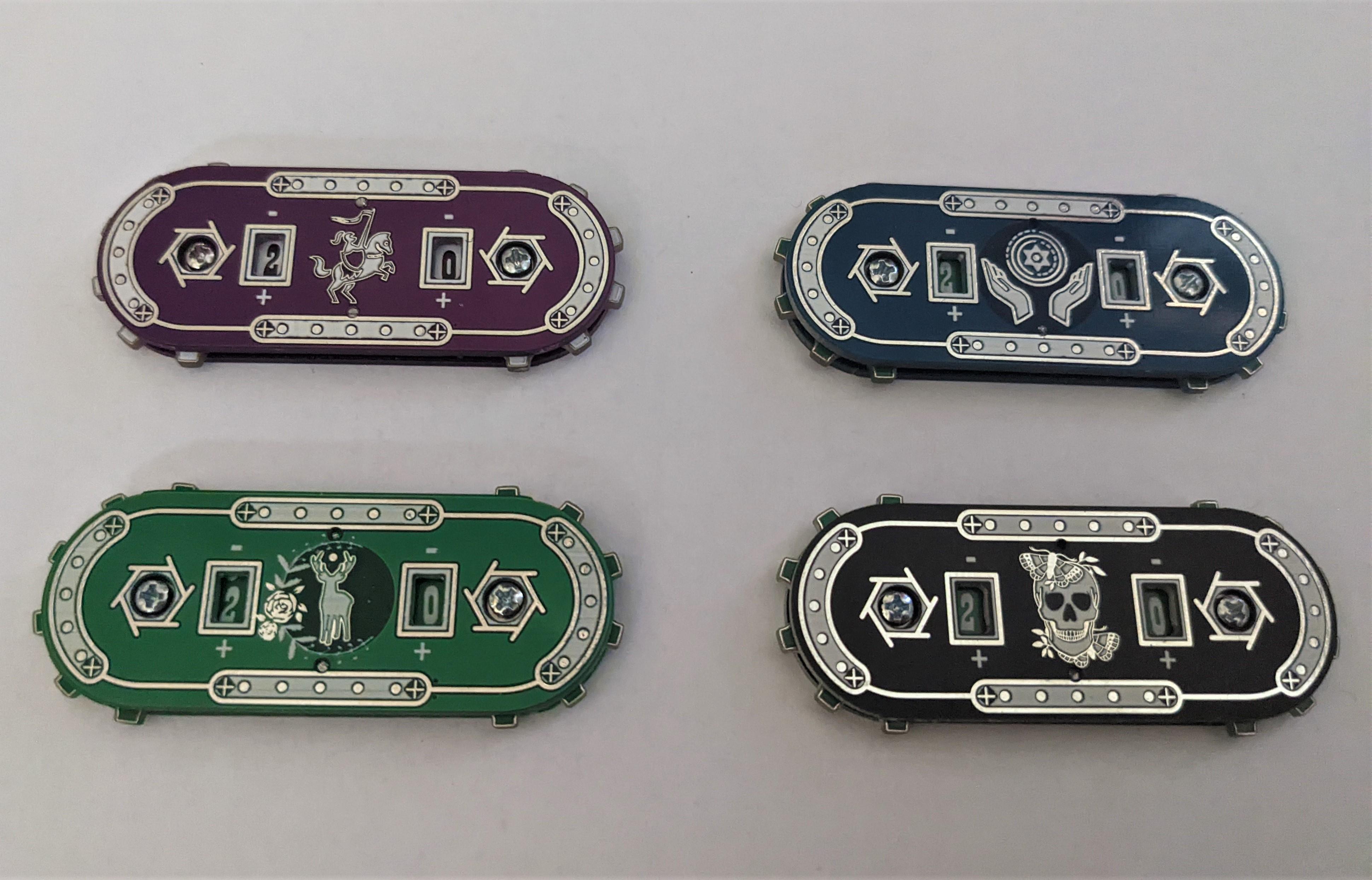
Printed circuit boards are ubiquitous through-out the electronics world. You'll probably find them inside almost every electronic device you own, and everyday more and more makers are incorporating them into their own projects. But have you ever considered using them for artistic purposes, such as pins, key-chains, badges, etc? PCBs are not only cheap (5 for $5 or less), they are durable, lightweight, and offer high dimensional accuracy. Streamlined ordering processes have become the industry standard, and there plenty of free tools available for designing them, no electronics knowledge required.
I believe that they're a useful tool for every maker to have in their playbook.
In this guide I'll walk through the core skills I use when designing artistic PCBs including:
- Board Layers and How to Use Them.
- Creating a Board Outline.
- Importing DXFs into EasyEDA.
- Creating and Preparing SVGs.
- Importing SVGs into EasyEDA.
- Traces and Outlining Images.
- Board Features (holes, solid regions, etc).
- Text and Fonts.
- Curved Text and the Inkscape Paint Bucket.
- Working with the Backside.
- Exporting Gerber Files.
- Ordering PCBs.
I'll try to offer as many tips and tricks as I can along the way.
For a practical example, I'll create a Destiny 2 inspired keychain/pin step by step as part of this guide (shout-out to any fellow Guardians out there!).
I've made the PCB publicly available so you can copy and tinker with it as you like.
You can find it here: Link to PCB.
If you have any questions, please leave a comment and I'll try to help.
Supplies
You won't need any physical tools for this Instructable, but you will need a number of software products. Because there are a variety of different software solutions you could use, I'll list what they need to be able to do, and then what I use.
All the programs and resources I use are free.
- A drafting or sketching program. This is for creating board outlines and sketching out board features. It should be able to draw 2D lines and curves, and let you set their dimensions. It also should be able to export SVGs or DXF files.
- I use Autodesk Fusion 360 (it's free for hobbists).
- A SVG creator/editor. This might be the same program as #1 depending on what you use. It should be able to create SVG's from images and edit existing SVGs.
- I use Inkscape.
- A PCB design program. Should be able to import SVGs. It is helpful if it allows you to create PCBs without needing a schematic.
- I use EasyEDA, which is a free browser program.
If you do use Fusion 360 and EasyEDA, you'll need to install a couple of plugins for working with SVGs and DXFs.
- Fusion 360: DXF (Spline to Polyline) and Shaper Utilities (for SVGs)
- EasyEDA: SVG Import.
Through-out this guide I'll use functions specific to Fusion 360, Inkscape, and EasyEDA. If you're using another prgram you'll need to figure out how to work it yourself.
This is also just how I make my designs. I'm always learning and there's probably faster ways to do some of the steps. I'll try to keep this instructable updated as I learn new things.
Board Layers and How to Use Them
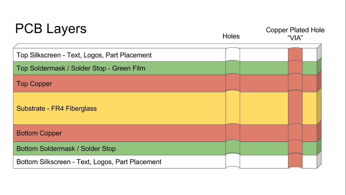
Before we begin designing, we should go over exactly what makes up a PCB, and how we can use each part.
PCBs are usually made up of four layers sandwiched on top of one another:
As shown in the image above, the layers are:
- The Substrate: Generally fiberglass or aluminum. This is core of the PCB, which provides rigidity to the board.
- The Copper: This is the conductive layer, used to make electrical connections.
- The Solder Mask: This layer covers up and protects the copper and raw fiberglass layers. It also gives the PCB its color.
- The Silkscreen: Almost always white, this is the upper most layer generally used for text and markings.
Double-sided PCBs are the default these days. They have a set of layers on both the top and bottom sides of the board. The sides are independent of one another, so you are free to have completely different designs on both sides.
Creating different features on each layer lets you to make detailed, intricate designs. Both the copper and solder mask layers are etched on, and offer high accuracy (6mil - 0.1524mm), while the silkscreen is painted or printed on and offers less accuracy, down to about 8mil.
As a rule of thumb, the smallest feature most PCB manufactures can reliably reproduce is a 6x6mil wide square.
For a more in-depth tour of PCBs, SparkFun has a good article here.
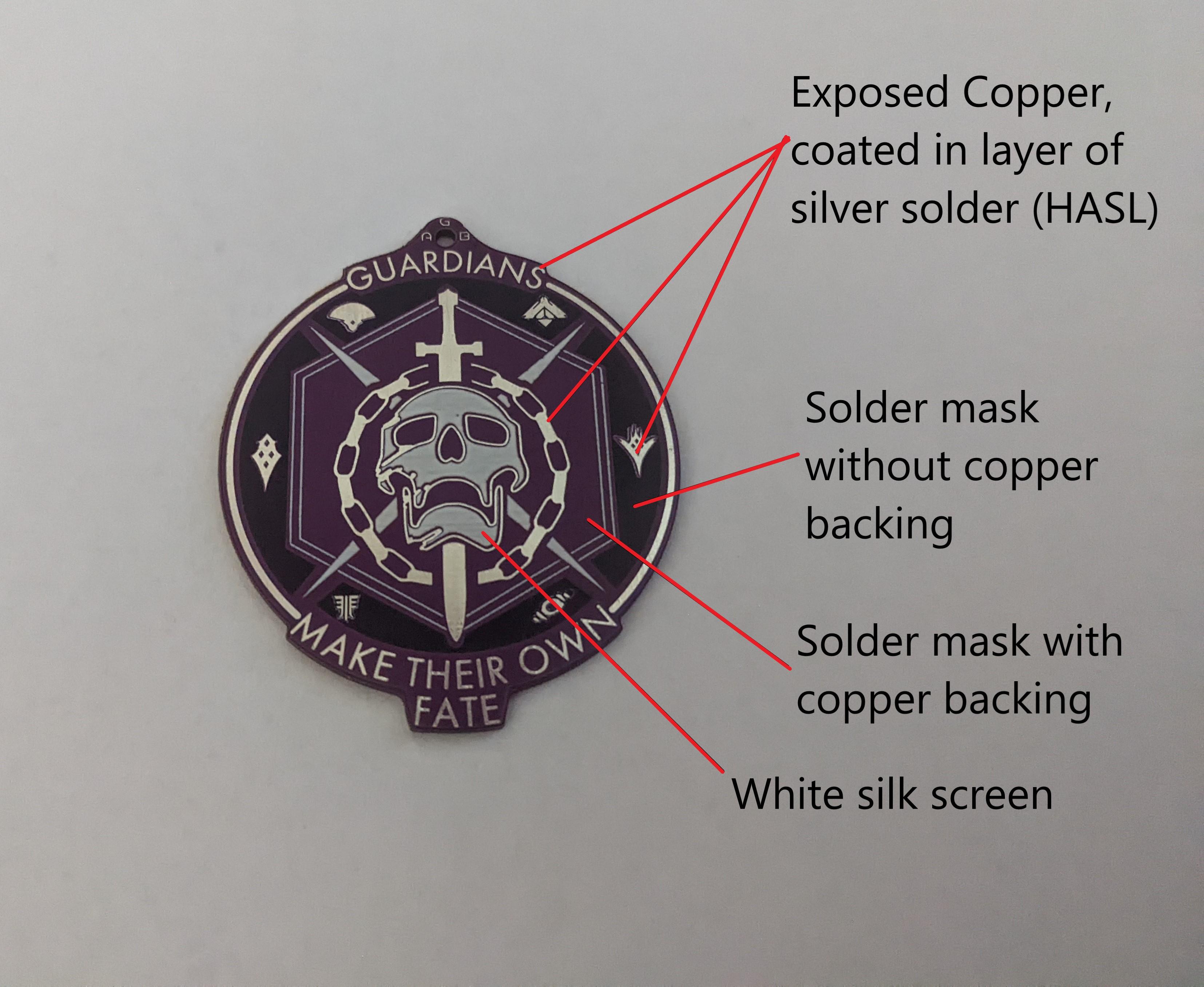
As you can see in the second image above, each of layer provides a different visual effect:
- The Substrate: Generally a yellow-tan color. Not very attractive in my opinion, but will let light through if using LEDs. (not pictured).
- The Copper: Copper under the solder mask will lighten up the silkscreen layer. You can also expose the copper to the air, which will automatically be coated in either solder or gold to prevent corrosion. This creates shiny silver or gold areas. Copper is added to the board either by using a copper pour or by placing items on the top/bottom layers.
- The Solder Mask: The main color for the board, available in green, red, blue, black, white, and sometimes purple. The exact colors will depend on the board manufacturer. By default, the entire PCB is covered in this layer. Placing features on this layer actually removes the solder mask from them, exposing what ever is underneath (ie copper or the substrate).
- The Silkscreen: Almost always white. Has a more painted-on look. It is the upper most layer, but will be over-ridden by any exposed copper below it.
Because you only have a few colors to work with, PCB art is probably best suited for making geometric designs, or re-creating logos/icons/silhouettes, etc.
Next I'll move on with a working example, and show you how I made my Destiny 2 pin/keychain step by step.
Creating a Board Outline

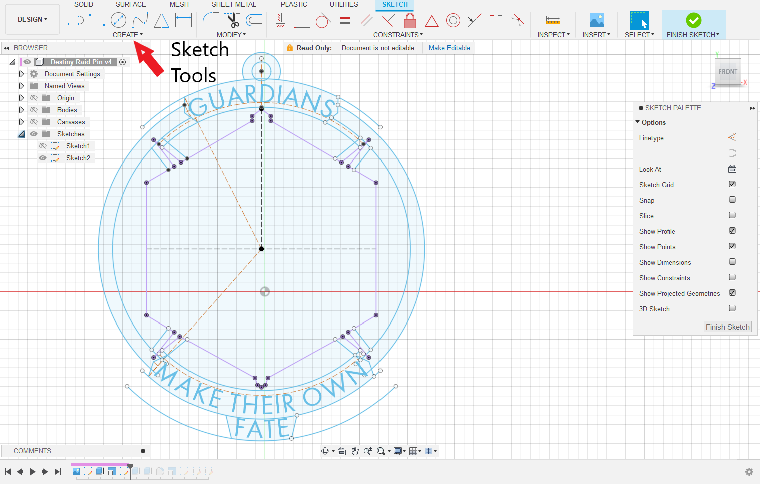
The first step to any PCB design is creating an outline of board. As the name implies, the outline designates the outer edge of the PCB. You can also have outlined regions within the board itself. These will be cut out of the board, making holes.
Unfortunately, while you can sketch a board outline in all PCB design programs, the sketching tools in EasyEDA (and most other EDA programs I think) are fairly basic. You cannot easily specify dimensions or constraints, and lines can become disconnected from one another, making for a frustrating experience when creating anything beyond basic shapes.
Instead, it's easier to use an external drafting program, such as Fusion 360, to create major board features.
Sketching in Fusion 360:
Begin by opening Fusion 360 and starting a new sketch by hitting the "new sketch' button on the top bar. Start the sketch by selecting any of the origin planes, it doesn't matter which one.
From here you can use the sketch tools to create your PCB outline. I won't go over the tools in detail, but you can watch here for a quick overview. I recommend sketching out pretty much all the boards features, including any holes, cutouts, etc. This will make it easier to change things later if needed. You can also add dimensions to your sketch objects using the "d" key. Make sure the outer board edge is a continuous closed line without breaks.
As you can see in the image above, I've created a sketch of my Destiny 2 PCB, including most of the major features of the board. The basis for my design is the skull-sword-chains symbol from the game. I started by importing an image of the symbol into Fusion 360 and then sketched around it, expanding my PCB design as I went.
I also included text as part of my sketch. However, in general I recommend creating as much text as possible in EasyEDA rather than Fusion 360. This saves you having to match up fonts between the two programs. Unfortunately, EasyEDA cannot do curved text along a line, so I had to use Fusion 360 (see Step 8-9 for more on text).
Exporting:
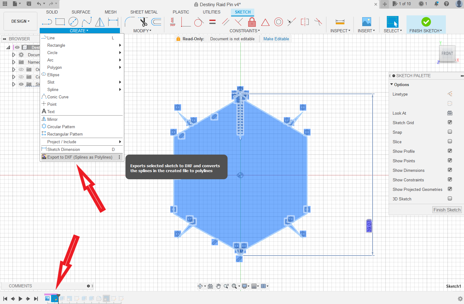
Once your sketch is complete, you can export it as a DXF file using the DXF (Spline to Polyline) tool. Using the tool is a little awkward. It's part of the sketch toolbar, so you must be editing a sketch to access it. From there, you must select the sketch you want to export in the bottom history bar. Upon exporting, it will ask for a tolerance; set it to something small, like 0.1mm. Some notes:
- You should use a DXF for the board outline rather than an SVG because EasyEDA always imports them at the correct scale (with the correct units selected), which is critical to the board outline.
- I do not use the native Fusion 360 DXF export tool because it seems to lose curves when I import it into EasyEDA.
To export SVGs you can use the Shaper Utilities plugin. This shows up under the Utilities tab in Fusion 360. It's fairly intuitive, but you can see a full tutorial here.
Before moving on to importing the DXF into EasyEDA I'll briefly cover exporting individual board features. You don't need to read this, but it may be helpful for complex designs.
Exporting Individual Features:
It can be useful to export individual sketch features as DXFs or SVGs. The easiest way to do this is to use the "project/include" tool in the Fusion 360 sketch tools menu. This lets you select lines from other sketches or bodies and include them in your current sketch. So you can create multiple sketches, each with a different intersected feature, which you can then export. These will all be tied back to the original sketch or body, so any changes made there will carried over to the new sketches. I used this method to separate out the inner holes and the text for the Destiny 2 PCB.
Importing DXFs Into EasyEDA
EasyEDA Overview:
Now that the board outline is complete, we need to import it into an Electronic Design Automation (EDA) program and begin fleshing out the PCB.
There are many different EDA programs available, but EasyEDA is what I use because it has been easy for me to learn, it's free, and it's browser based, so you can access your designs from anywhere.
Before we start I'll go over the EasyEDA interface briefly. You should open EasyEDA and start a new PCB design using the drop-down menu under "file".
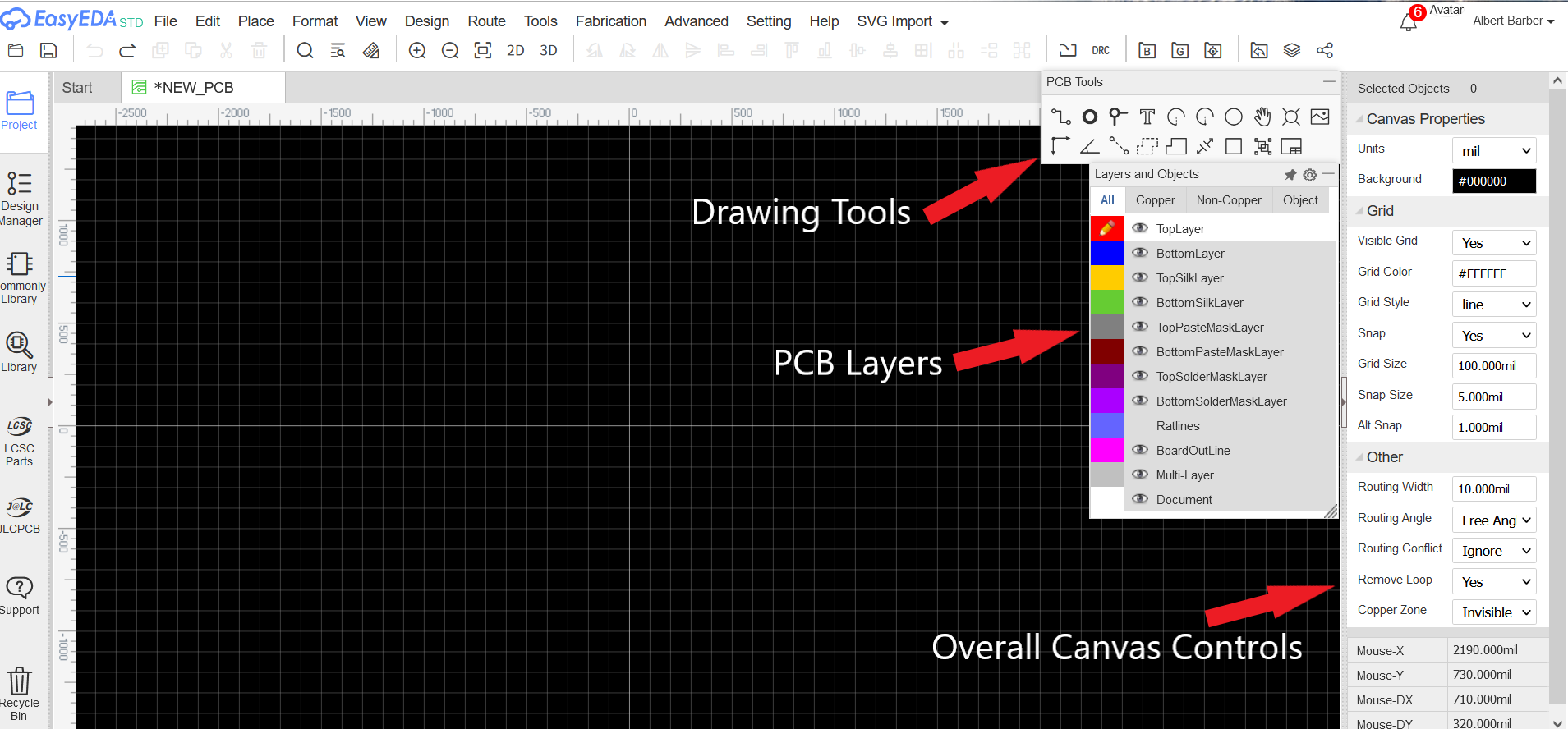
Once you start a PCB you'll be taken to the PCB design canvas. There are three menus on the right-hand side of the screen that you'll want to become familiar with: "PCB Tools", "Layers and Objects", and "Canvas Properties". You'll use these menus frequently when designing PCBs.
The "PCB Tools" menu contains drawing tools commonly used in PCB design. This is where you add features to your PCB. I'll go over each of the tools as we need them.
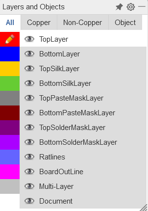
The "Layers and Objects" menu lists all the layers on the PCB for both the top and bottom sides. You use this menu to both hide/show layers and to set what layer you're drawing on.
Some quick notes:
- Each layer is color coded so you can quickly identify what features are on what layer.
- You can toggle each layer's visibility using the eyeball icon.
- The layer you're currently drawing on is marked with a pencil icon, you can click on other layers to switch to them.
- The Top and Bottom layers are the copper layers. Anything on these layers will be etched from copper.
- You can ignore the top and bottom paste layer and the ratlines.
- The multi-layer layer displays features that go through the whole board, such as holes and cutouts.
- The document layer is for notes; anything on this layer will be excluded from the final PCB file.
The "Canvas Properties" menu sets properties for the whole canvas.
I recommend adjusting following settings:
- Set the Alt-snap value to 1 mil. This sets the snapping of objects when holding down the Alt key. The default 5mil is too coarse when working with SVG images.
- Change the routing angle to "Free angle". This prevents lines from forming 45 deg corners (useful in electronics, but not as much for free-hand drawing)
- You can change the document units to mm if you like. I keep mine as mil because I'm used to it.
You can select multiple features by holding Ctrl. Hitting the space-bar will rotate features 90deg.
Importing A Board Outline:
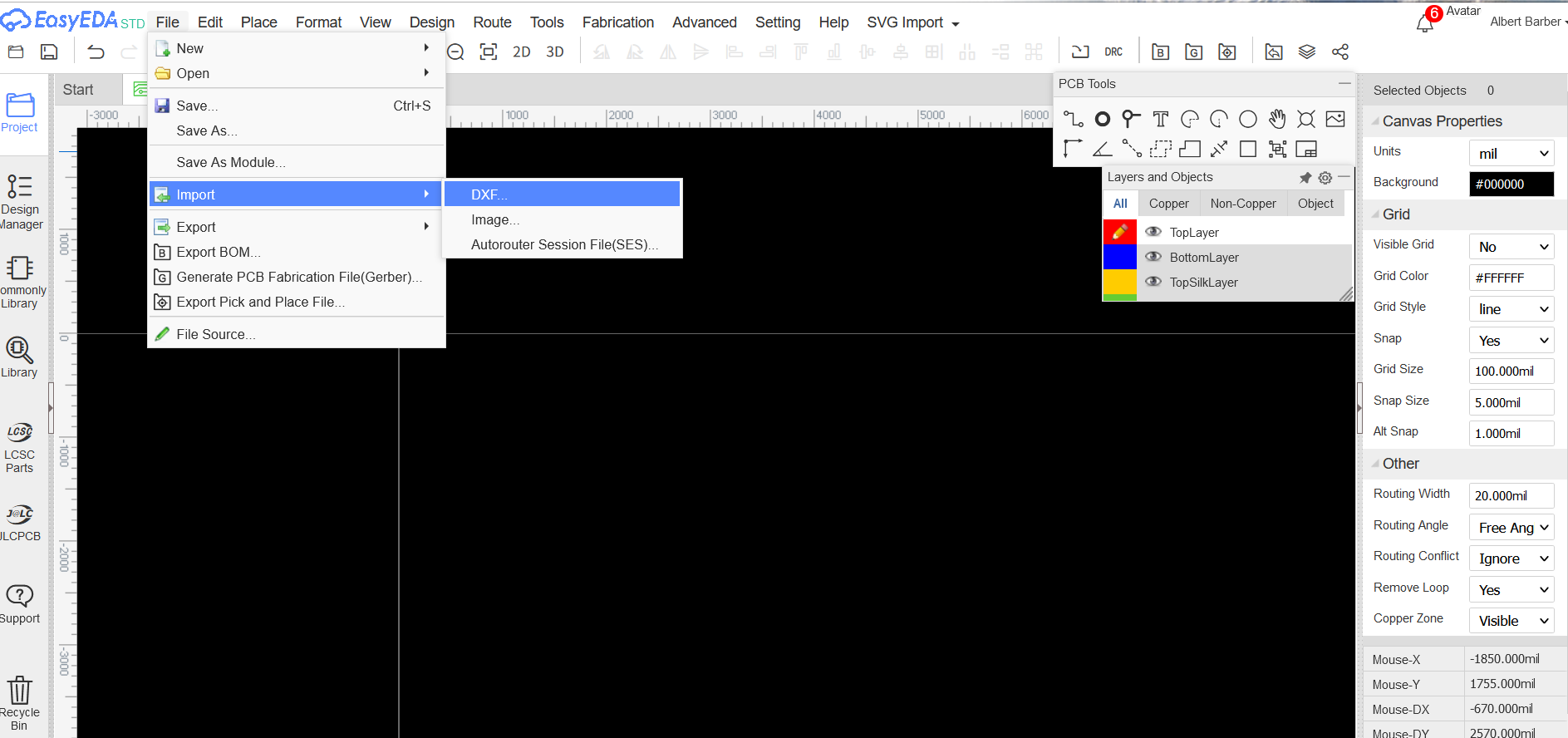
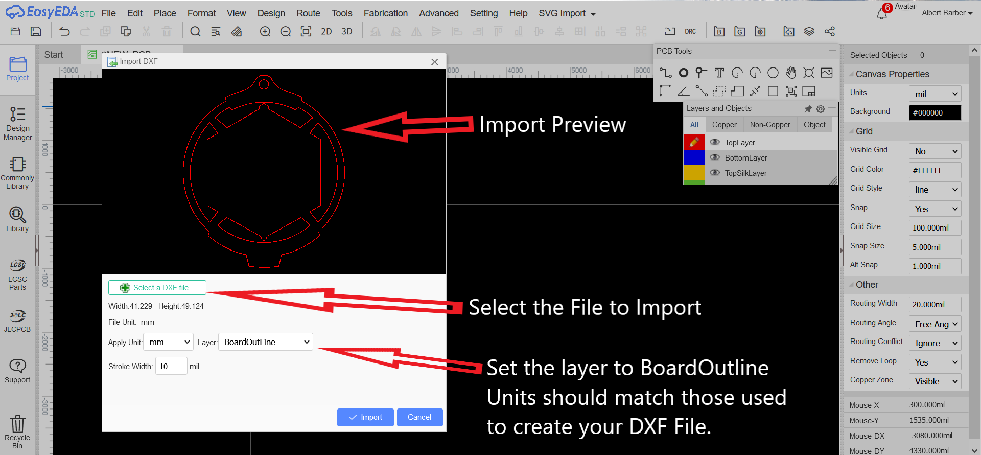
Once you are comfortable, you can import your PCB outline. Do this by going File->Import->DXF, select your file using the dialog box. Make sure the layer is set to board outline, and the units match those in Fusion 360 (should be mm). You can set the trace width (outline thickness) down to 4mil or less because we want to maximize the drawing space on the board.
SVGs tend to be imported around the origin point, so I like to place my board outline off to one side to make SVGs easier to select.
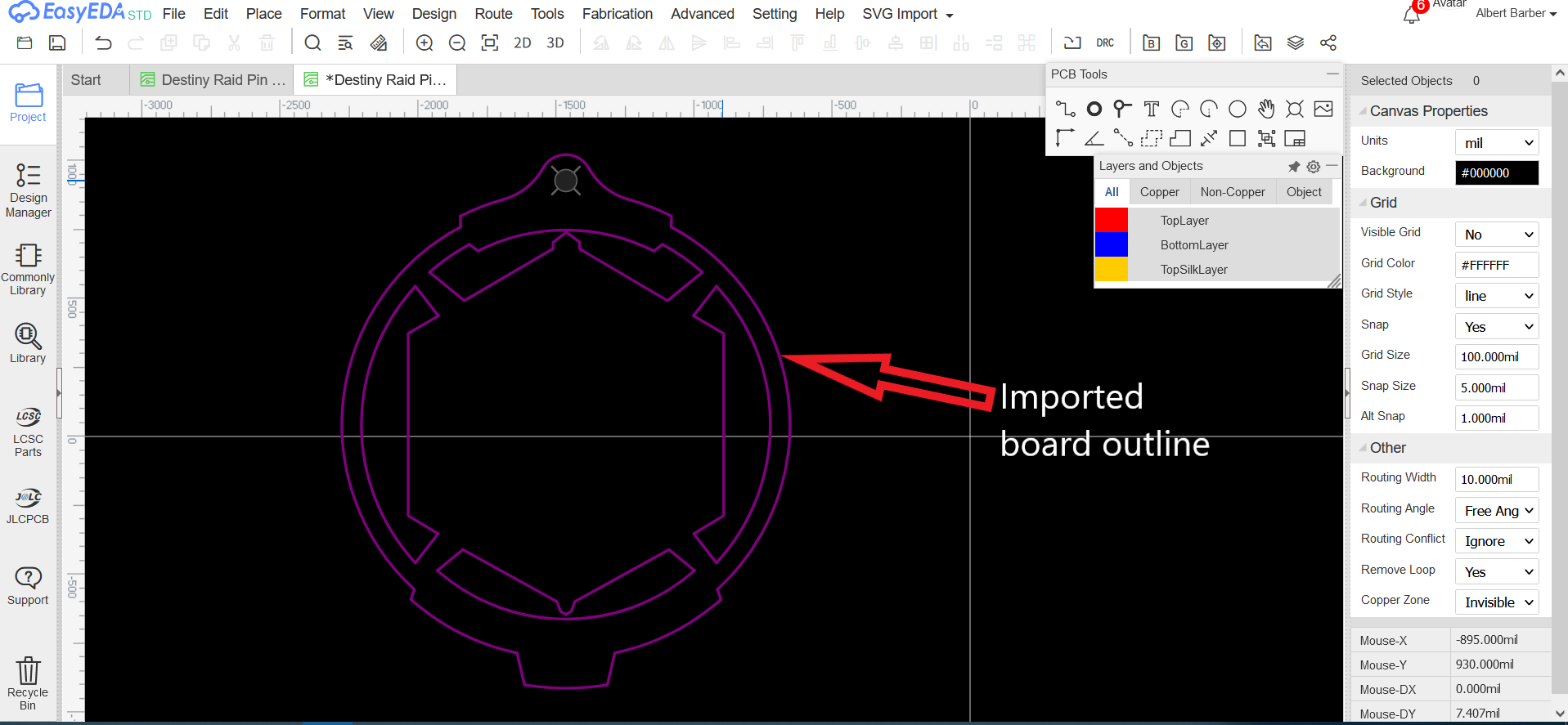
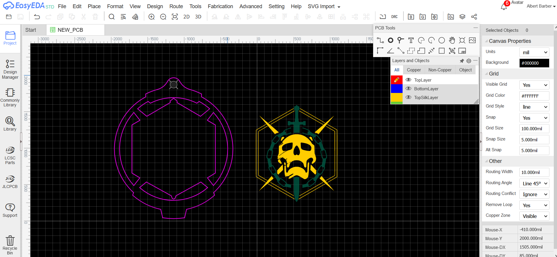
For my Destiny 2 PCB, I import the board outline sketch that I created in the previous step and place it on the canvas. I've left the trace width as 10mil for visibility.
Next we'll convert any images we need into SVGs and add them to the PCB.
Creating and Preparing SVGs

Converting Images to SVGs:
The easiest way to add art to a PCB is with an image. Although EasyEDA does allow you to import images directly, it tends to oversimplify them, removing detail. It's much more reliable to convert images into SVGs and then import them.
To convert images I use Inkscape, which is a free and robust vector editing program.
To begin, you'll need to find an image.
Ideally you image should be a crisp and mono-color, like a logo. We want to reduce the it down to a black and white silhouette, so the closer you start to that the better. If you can find a pre-made SVG you can skip the conversion process altogether. There are lots of free SVG sites out there, although they mostly host generic SVGs.
So hone your Google-fu and get searching.
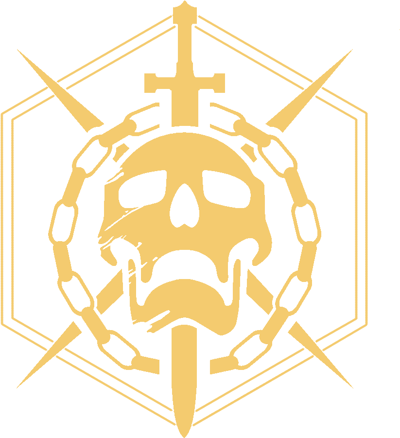
For the Destiny 2 PCB, I found a clean image of the skull-sword-chains symbol I'd like to use.
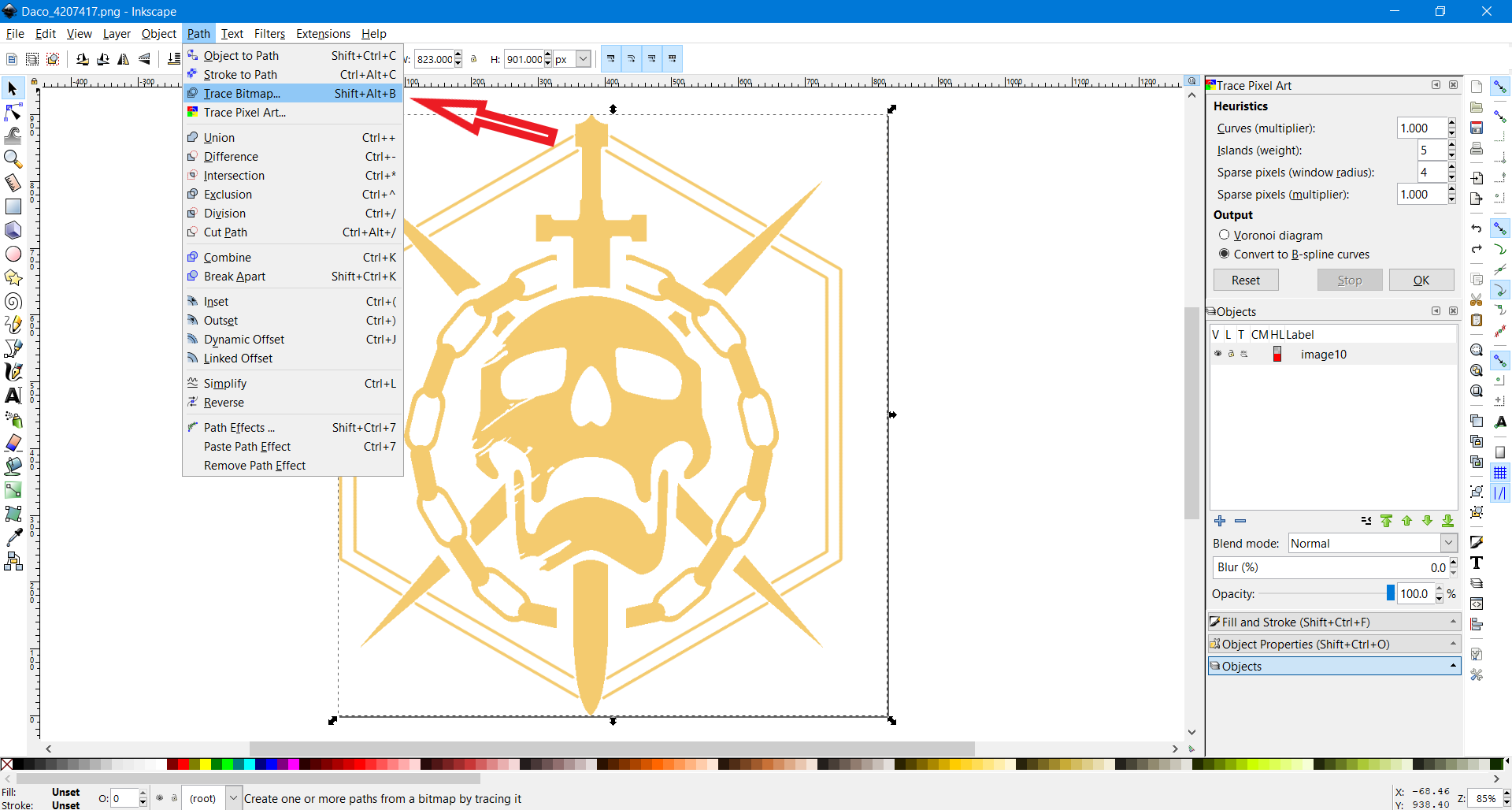
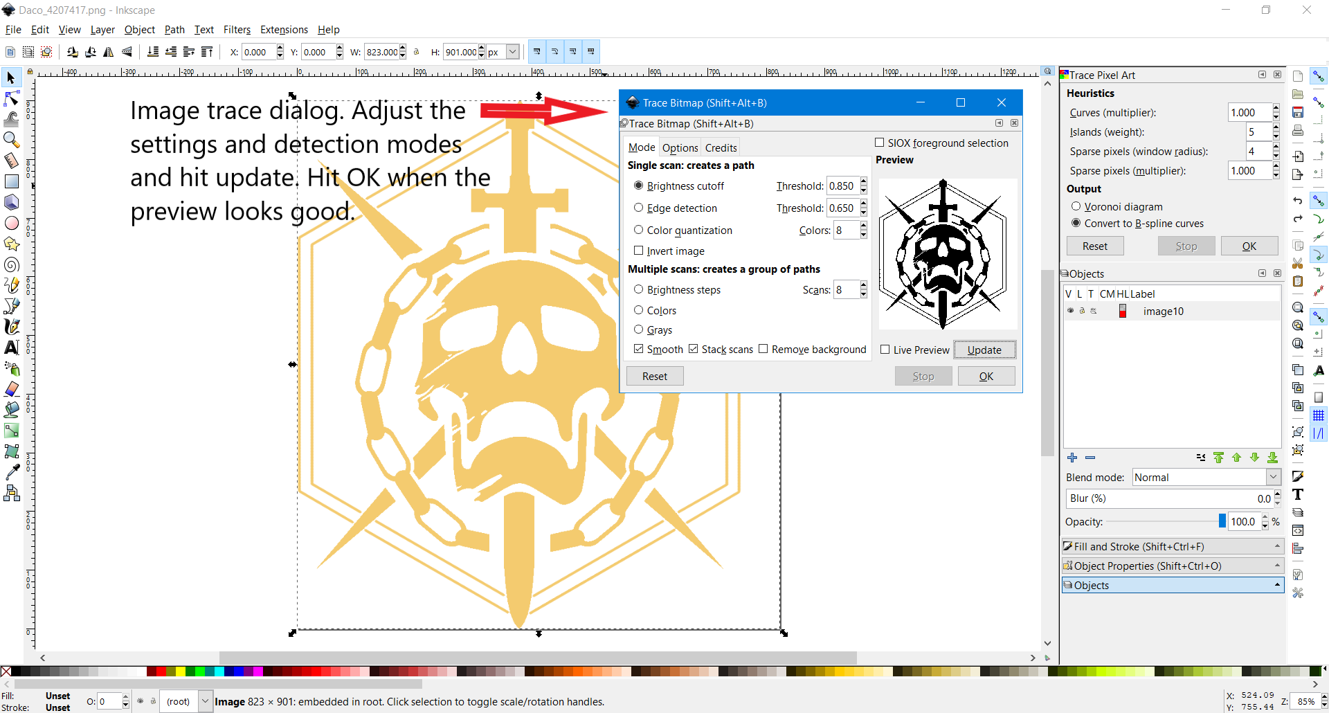
Open your image with Inkscape. We want to trace the image to make a silhouette:
- Under the "path" menu, select "Bitmap to Path".
- A dialog box should pop up with some options.
- Make sure you have the image selected.
- By hitting "update" in the dialog box you'll get a preview of the traced image
- Test out different settings until you get a clean looking preview. Every image is different, so there's no one tracing method that works the best.
- To help preserve sharp corners you can try dialing down the smoothing to about 0.6-0.8.
You may need to go back and forth a few times with different settings until you get something you're happy with. The end goal is to produce a filled black and white silhouette of your image. If you need to fill in parts of the result you can use the paint bucket tool (see Step 10 for details).
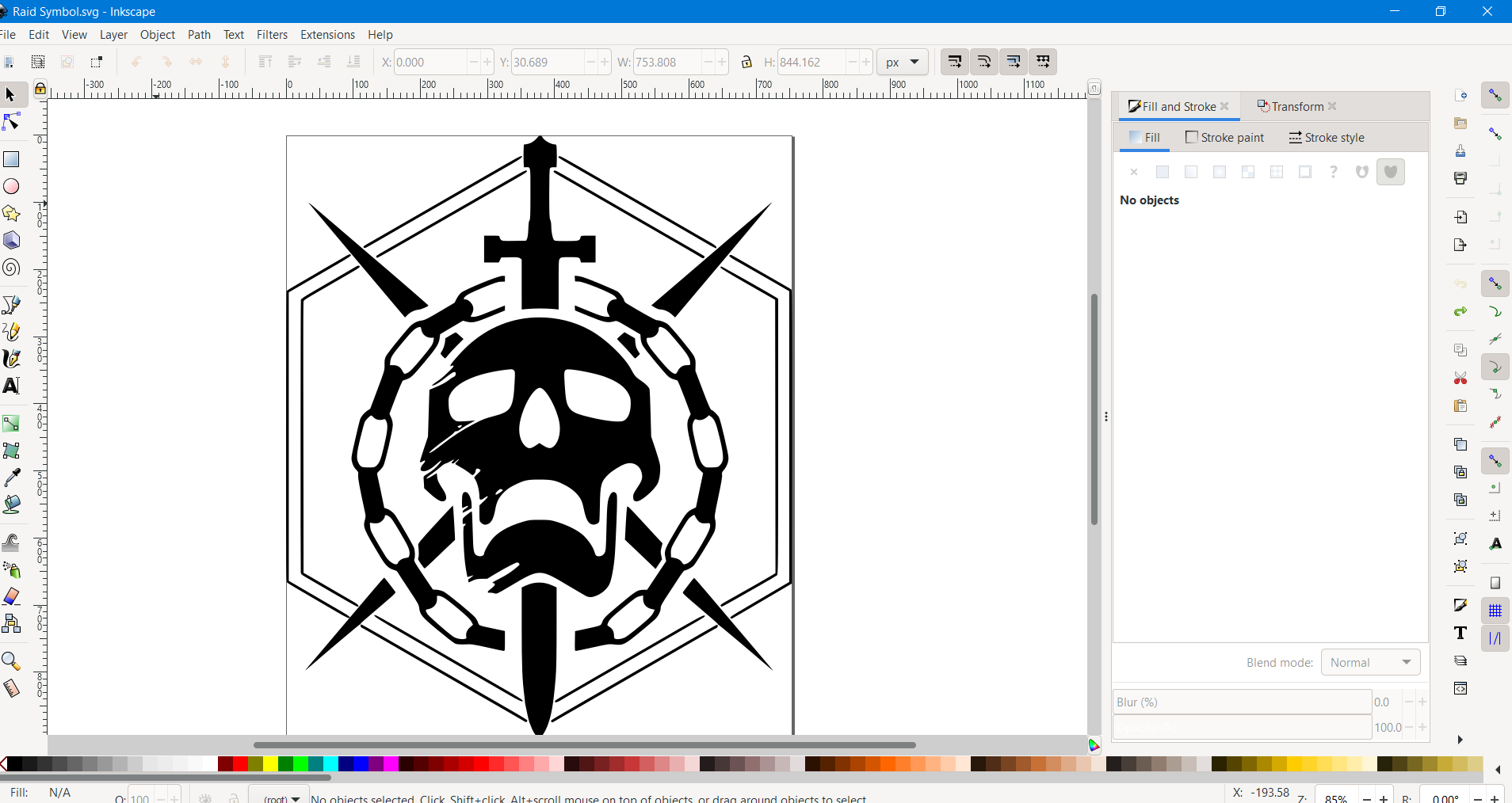
Once you're finished, you can delete the original image from Inkscape and save the file as an SVG.
You can see an image of my final skull-sword-chains SVG in Inkscape above.
Splitting/Combining SVG Parts:
If you'd like different parts of your SVG to be on different PCB layers (ex some parts on the silver solder mask layer and others on the silk screen) you can split the SVG into separate bodies:
- Under the "path" menu, select break apart with your SVG selected
- Your SVG will be split into separate paths.
- If your image has holes, they may be filled in. There should be separate parts for the hole and the filled body. Select both and then under the "path" menu select "exclusion" or one of the other boolean operation options.
- Hopefully one of the options will work to restore the holes to your image.
You can re-combine separate bodies under "path", "combine".
For my skull-sword-chains symbol, I knew that I wanted the chains and the sword to be silver solder mask, while keeping the other parts silkscreen white. So I separated the SVG, and then re-combined it into two groups: one with the sword and the chains, and one with all the other parts. The cutouts in the chains and the skull's eyes did get filled when I did the split, so I had to boolean exclude them back together.
Next we'll move onto importing the SVGs into EasyEDA.
Importing SVGs Into EasyEDA

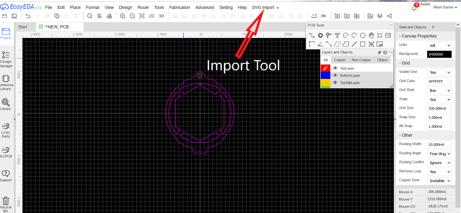
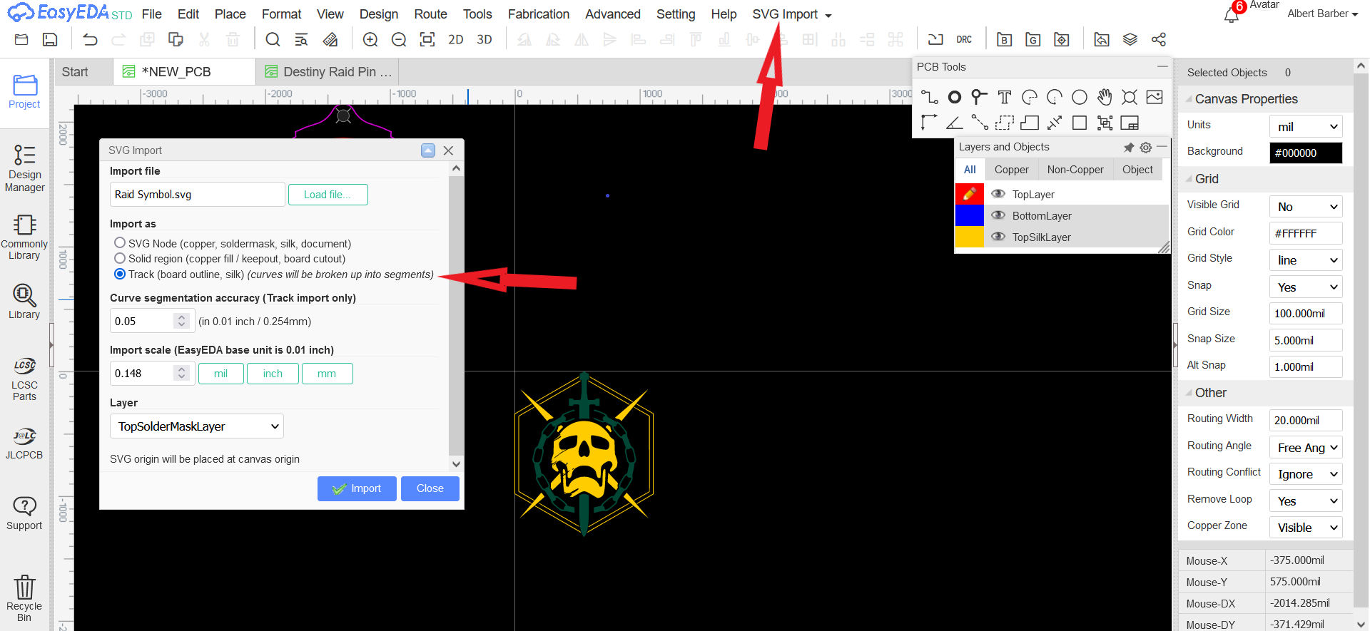
EasyEDA does not natively support importing SVG, but the SVG Import extension adds the functionality. The extension should appear at the end of the top menu bar in your EasyEDA workspace.
You can find more info and installation instructions for the import tool at the author's Github.
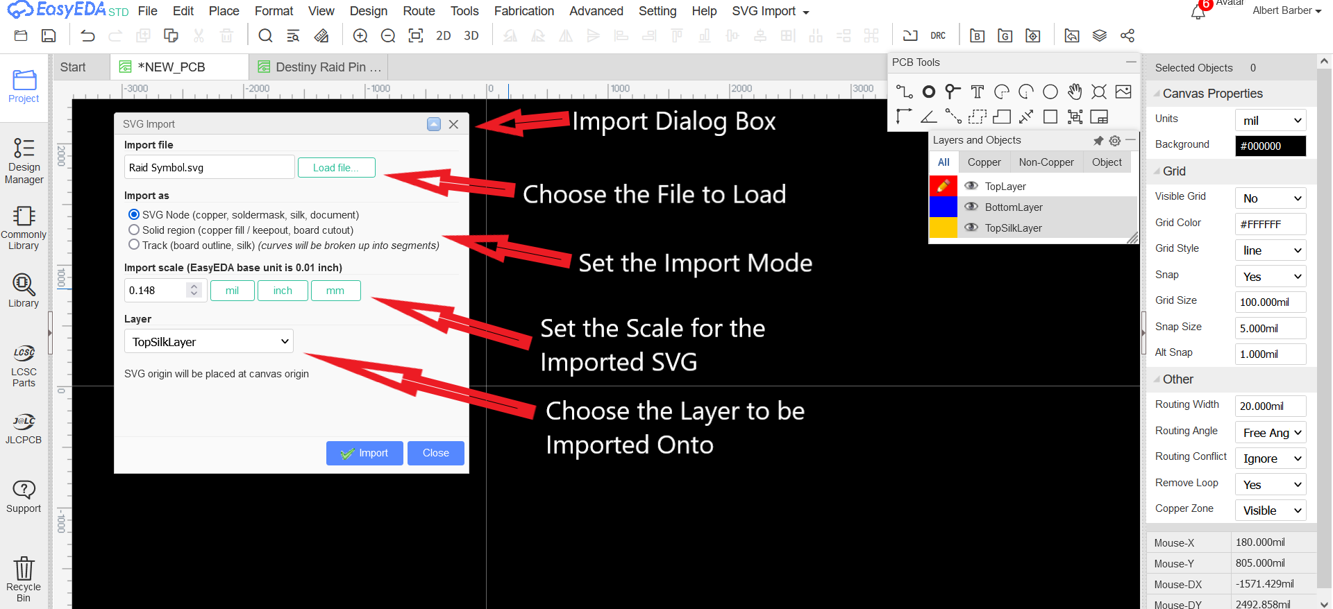
To import an SVG, hover over the extension and select "Open Import Dialog". This should bring up a dialog box. In the dialog box click "load file", and select the SVG file you'd like to load.
Now you have three options for how to import the SVG:
- SVG Node: This loads the SVG as an image. Generally good if you'd like the SVG to be on one (or more) of the main board layers (silk-screen, copper, etc).
- Solid Region: Loads the SVG as a set of nodes, forming a solid polygon. At the time of writing, it cannot handle SVGs made up of multiple bodies; only a part of the SVG will be loaded. Instead I recommend using option 3.
- Track: This will load the outline of the SVG. The width of the of the outline will be your default routing/trace width. The outline will be larger than your original image, which is useful for adding a border to around you SVGs. You can also convert the outline into a board cutout, solid region, etc (I go over these features in more detail in Steps 6 and 7)
Before adjusting the scale, set the layer at the bottom of the dialog box. If your SVG has multiple parts, choose the layer that most of the parts are on.
Next you'll have to set the import scale. Getting the correct scale value is tricky. I just tend to try the default, and then either increase or decrease it accordingly. You can probably calculate the scale based on the size of the SVG in Inkscape, but I find trial and error to be easier, especially when you don't know exactly how big you'd like the image to be.
When you hit import, a confirmation notification should popup in the lower left hand corner. If it doesn't, your SVG probably isn't manifold. If you get the confirmation, but you don't see an image, you may have one (or more) of these problems:
- Your image is too big. Try undoing, and reducing the scale.
- Your image is too small. You can try to find it by dragging a selection box around the canvas origin. The right side canvas properties panel will change if you find something. Try undoing, and increase the scale.
- Your image's origin is far away from 0. This can be really annoying. Try zooming out and scrolling around to find it. You can adjust the image's origin using Inkscape: see here.
Finally, sometimes the image imports on top of your PCB. This can make it annoying to select and move the image. I recommend selecting all the existing board features and shifting them away from the image and the re-importing. It doesn't matter where on the canvas the board is.
Once you've imported the image, you can select parts of it to change its layers using the object properites menu on the right-hand side of the screen.
For the Destiny 2 PCB, I imported the skull-sword-chains symbol image as an SVG Node on the Top Silk-screen layer. I wanted the chains and the sword to be silver, so I moved them to the Top Solder Mask layer. See the images for the final result (note that I've changed the color or my solder mask layers to teal to make them more visible, yours will be dark purple).
I've not moved the image because I want to give the skull a silver outline. I'll cover how to do this in the next step.
Traces and Outlining Images

Traces:
If you examine a PCB you'll undoubtedly see numerous traces (tracks) running like a spiders web across the board. These are lines of copper that form electrical connections between components. Because creating traces is so common, every line you draw on a PCB will use your current trace settings, even if it's not on the copper layer. By default EasyEDA sets the trace width to 10mil and the corner angle to 45 deg. You can adjust these settings in the right-hand "Canvas Properties" Menu. I find that a trace width of 15 - 30+mil, with 20 being your default, will give you clearly visible lines.
Be sure to put your traces on the top or bottom solder mask layer if you'd like them to be exposed silver or gold. If you leave them on the Top or Bottom layers, they'll be put under the solder mask, like normal PCB traces.
When selected, each line's properties are shown in the menu on the right-hand side of the screen. Here you can adjust the line's width and what layer it's on.
Like most EDAs, EasyEDA's line tools are pretty basic. They are really just intended to get from point A to point B without much fuss. You can add arcs, circles, and you can double click on lines to add more bend points, but creating something like a spline is impossible.
Outlining with Traces:
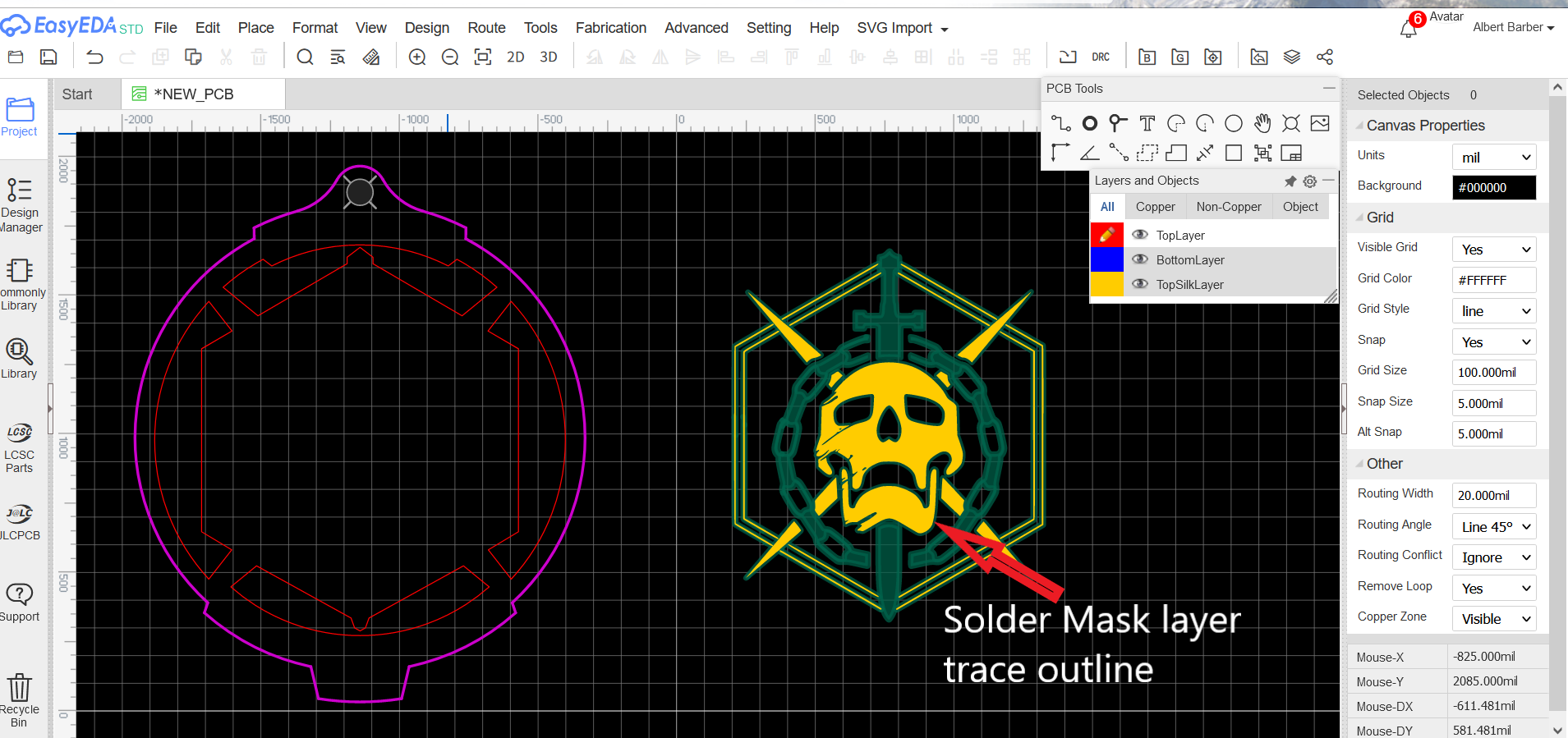
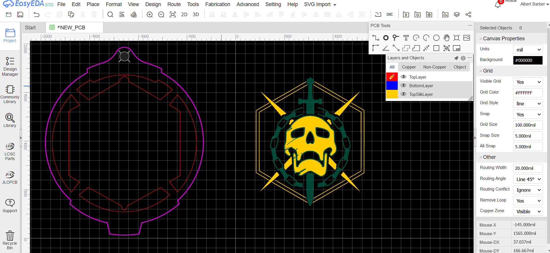
A handy trick I've found is to use exposed copper traces to outline silk-screen images. Silk-screen tends to have a fuzzy outline, so covering it up with a crisp trace sharpens it up. After you import an SVG as an SVG Node (see Step 5) leave the image in place. Next, import the image again as a track, setting the layer to the Top/Bottom Solder-Mask. This will create a set of silver traces outlining the image. You can then drag select the whole thing and move it where you want it.
There will be some overlap between the trace outline and the image, so don't use this technique on images with small details. Remember that the solder mask layer will over-write any silk-screen!
For the Destiny 2 PCB I added an outline to the central skull by importing it as an track (width 20mil) and then deleting all the extra traces around the chains and spikes.
More Board Features
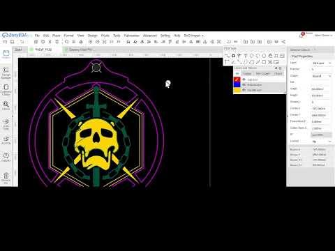
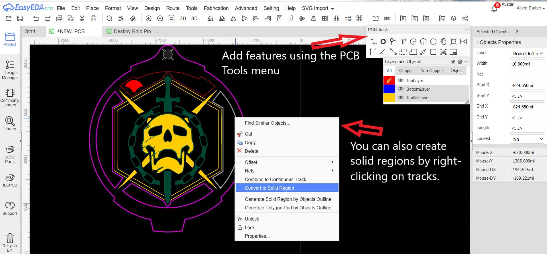
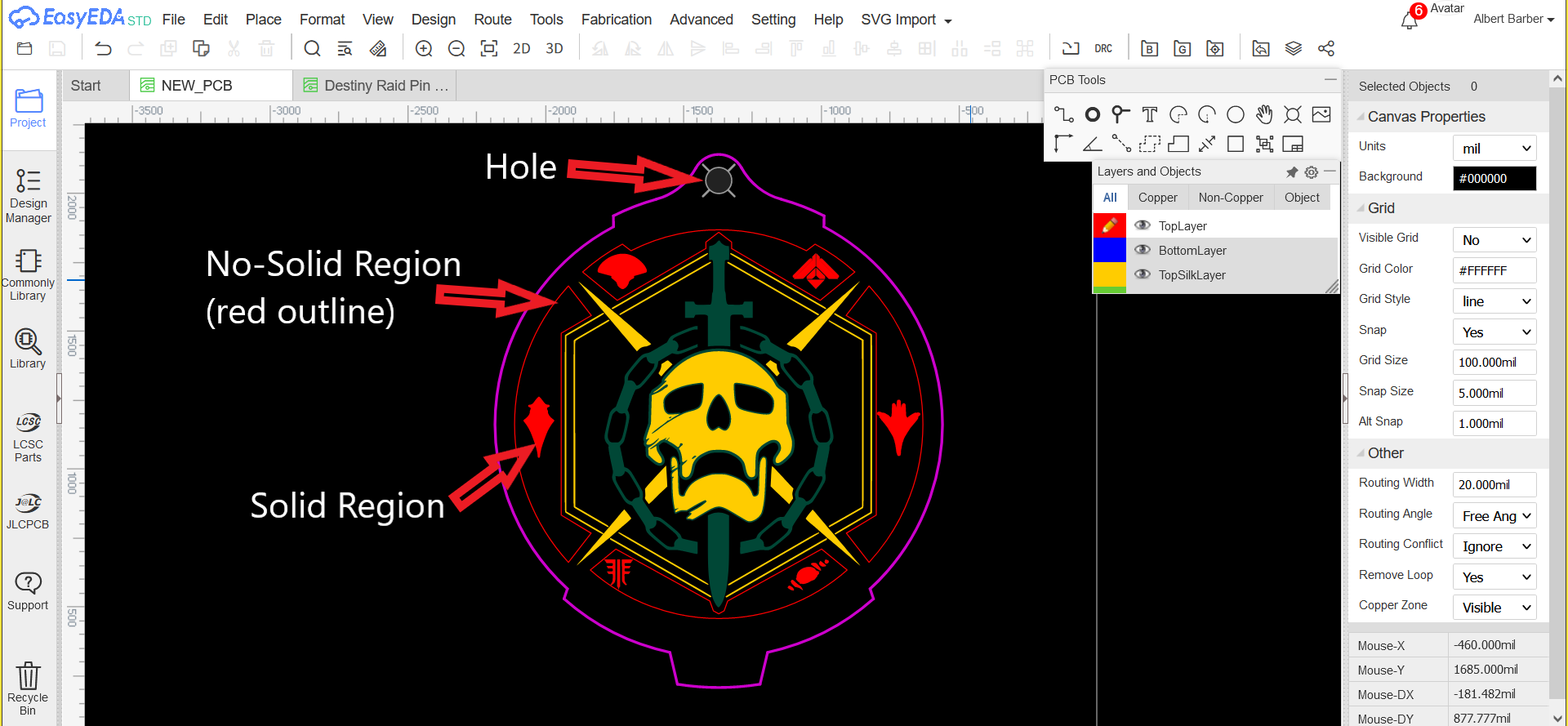
While tracks are the most common board feature, there are a number of others you may need to use. You can create all of these using the EasyEDA PCB Tools Menu.
- Holes: Circular holes through the entire PCB. They can be automatically created from sketch holes when you import a DXF file. They appear as part of the multi-layer layer. On the Canvas the "X" over them approximates the diameter of a screw head. On the Destiny 2 PCB I added a hole at the top of the board for a keyring.
- Board Cutouts: These the same as holes except they can be any shape and size. I go over how to create these below.
- Solid regions: An enclosed area that is either set to be filled or devoid of copper. Created in the same method as board cutouts.
- Pads: A shortcut for making a circular or rectangular area of exposed copper. Can also be set to include a hole. Not super useful for art, but these are the most common way to attach electrical components to a PCB.
- Vias: Very small copper plated holes through the PCB that form an electrical bridge between the front and back sides. They are usually covered by the solder mask, but are lightly visible. Probably not very useful artistically, but you may need to add at least one to your board (see Step 10).
- Copper Area: Usually used to add copper to the entire side of the PCB. I use this tool as part of my final design steps, see Step 10 for more info.
Creating Cutouts and Solid Regions:
Cutouts and solid regions can all be created in one of two ways:
- Via the solid region tool in the PCB Tools box. You place down points manually to form a polygon. You cannot add curves to it.
- By selecting a group of traces so that they form an enclosed shape, then right-clicking and selecting "convert to solid region". I generally use this method because most of my regions are imported from my Fusion 360 sketch.
By default, the solid region will be created as an area of copper. The area will be placed on the top layer, under the solder mask. If you want to create an area of exposed copper, set solid region's layer to either the top or bottom solder mask layer. You can also click on "expose copper" in the area's properties menu. This adds a solder mask layer underneath the area.
You can change any solid region to board cutout or no-solid by selecting it and then changing the type in the selected objects menu on the right-hand side of the screen. Note that no-solid means that copper pours will ignore the area (see Step 10), but any copper areas that are manually placed inside the area will still be created. No-solid regions will still be coated in the board-colored solder mask, but because they lack the copper backing, they create a darker color.
For the Destiny 2 PCB I wanted to create some no-solid regions between the skull-sword-chains symbol's spikes to add some color contrast to the PCB. I had already drawn the regions in Fusion 360 -- they were imported as part of the board outline. I do this by following the second method above.
I then added some additional symbols inside the copper areas. These were converted from images (Step 4-5). I wanted them to be exposed copper, so I imported them as tracks, converted them into solid regions, and then hit expose copper in the right-hand menu, adding a solder-mask layer to them automatically.
Text and Fonts
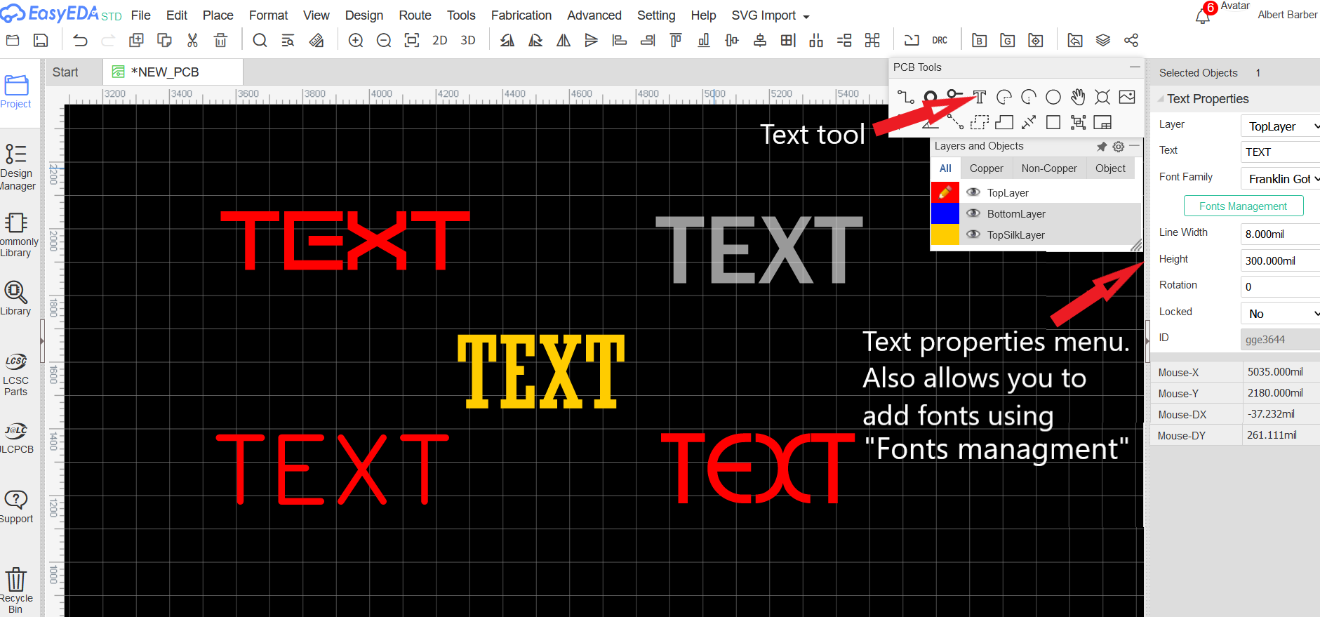
You can add text to your PCB using the text tool in the EasyEDA PCB Tools menu. As with most other features, you can place text on any layer of the board.
In EasyEDA you don't set the font size by pt, as you would do in a word processing program, instead you directly set its height. I find that heights of 50 - 100+mil produce clear, legible text.
To add a little pizzazz to your designs, you can import new fonts right into EasyEDA using .tff files. You can find thousands of these fonts files for free all over the web at sites like 1001freefonts.com or DaFont.com. To add a font, you'll first need to add a bit of text somewhere on your EasyEDA Canvas. Select the text, and in the right-hand side Text Properties menu hit "Fonts Management". This brings up a dialog box where you can add fonts to EasyEDA from your computer. Once a font is added, it's saved permanently in EasyEDA, making it available for all your PCB designs.
I should add that not all fonts may be suitable for PCBs. Fonts with intricate designs, or thin features may not be able to be drawn properly at smaller sizes. As a rule of thumb, the smallest feature most PCB manufactures can reliable reproduce is a 6x6mil square.
I've added an image to this step of some different fonts on different layers, including the Text Properties Menu.
Unfortunately, for my Destiny 2 PCB, I wanted most of the text to be along a curve. You cannot do this in EasyEDA, so I had to do it in Fusion 360 and then import it. I go over this in the next step.
Curved Text and the Inkscape Paint Bucket

Curved Text:
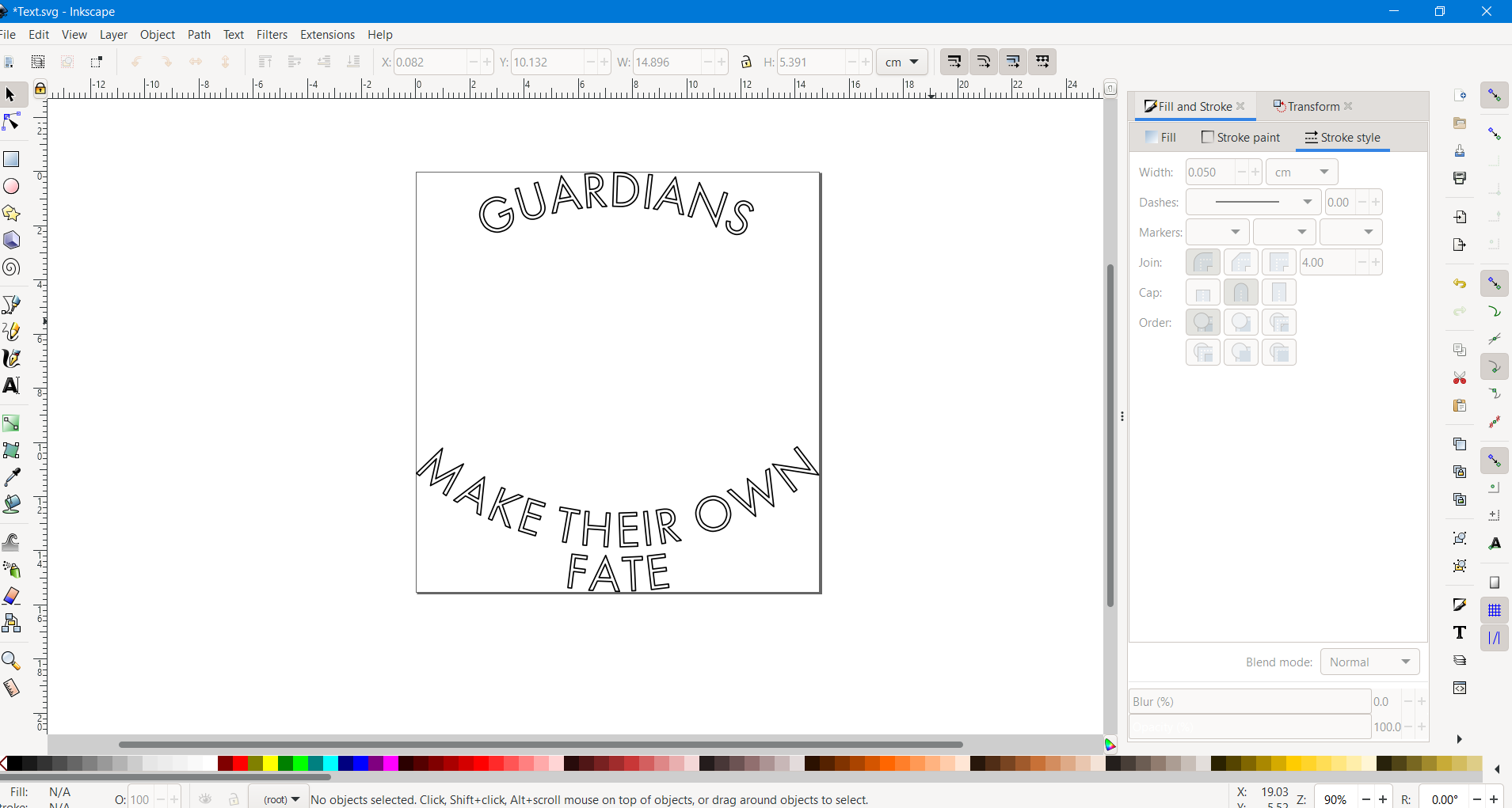
EasyEDA doesn't have the ability to create text along paths. For most designs this isn't needed, but for my Destiny 2 PCB I wanted the top and bottom text to be curved. In Fusion 360, you create text as part of a sketch, which gives you the option of attaching it to path. This should be fairly straight-forward, but for a full text tutorial, see this video. You can then export the text as an SVG by projecting it and then using the Shaper Origin plugin (see Step 2).
The text will be exported as an outline, see the image of my text export as an example. EasyEDA will not fill it in when you import it: you must do it manually using the Inkscape paint bucket tool.
The Inkscape Paintbucket Tool:
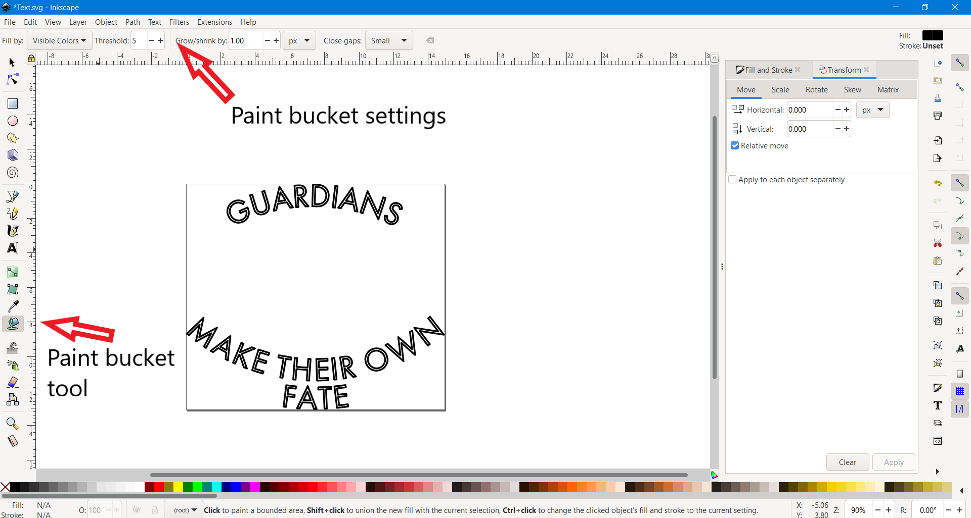
If you've ever used a paint program before, the paint bucket should be familiar; clicking it within an outline fills it with the paint bucket's color. By default, Inkscape's paint bucket will try to round out internal corners, leaving voids. To fix this you'll need to increase the "grow/shrink by" value of the paint bucket located in the top-left of the screen.
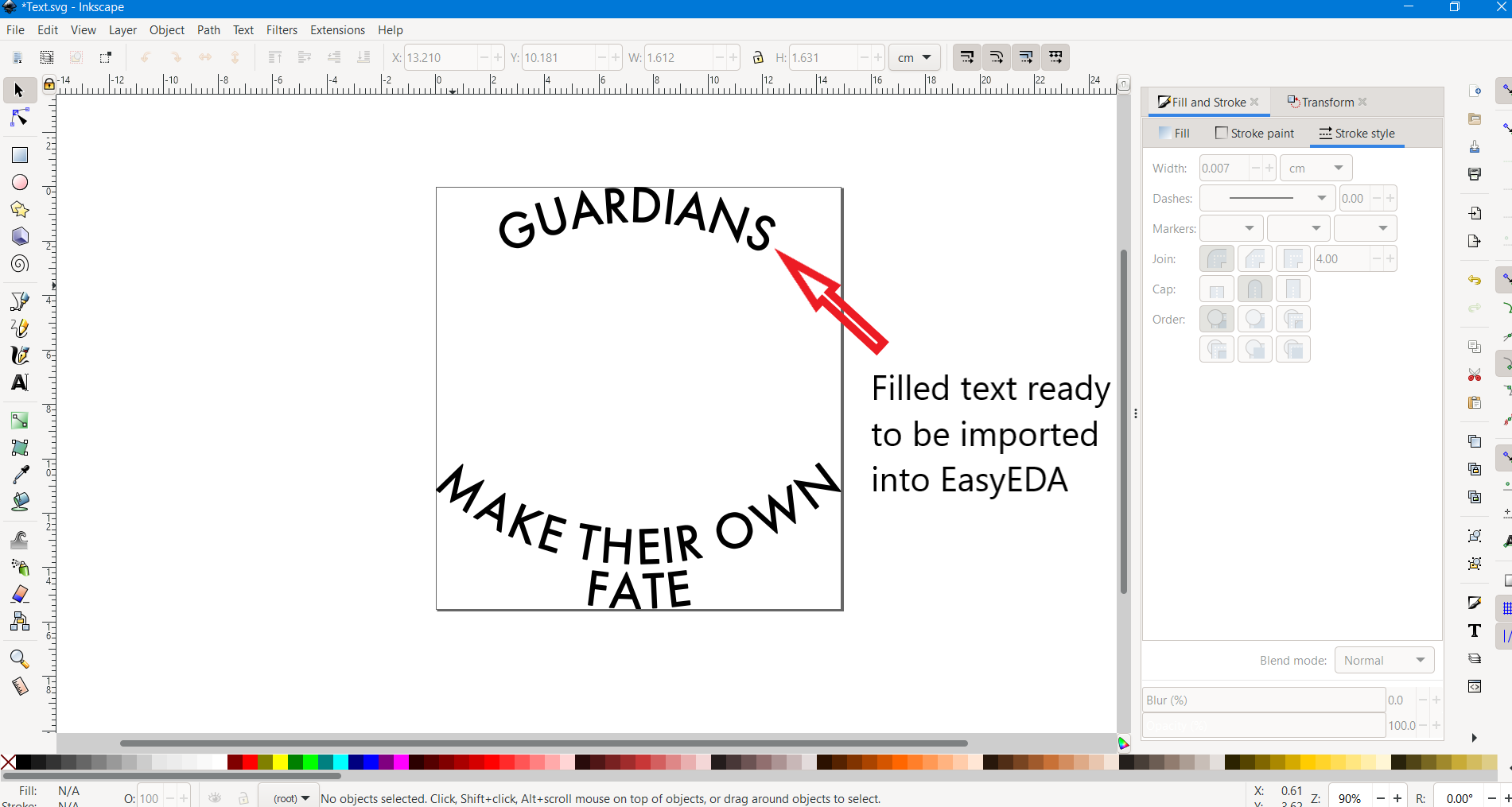
The filled area is treated as a separate region in Inkscape. To join it to the letters use "combine" under "path", as explained in Step 4.
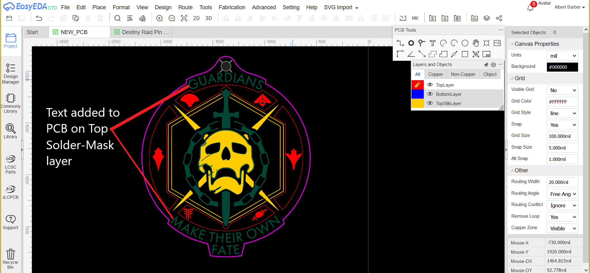
After filling in the text for my Destiny 2 PCB, I imported it into EasyEDA (Step 5) and placed in on the PCB.
Working With the Bottom Layers

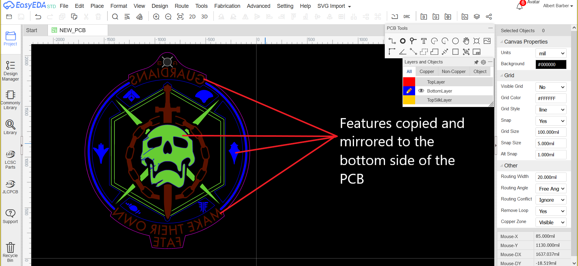
Modern PCBs have at least two copper layers, one on the bottom and one of the top. In terms of design, both layers are identical; anything you can do on the top layer, you can do on the bottom. So you can leave the bottom blank, replicate your top side design onto it, or create a completely different design.
In EasyEDA there is no change in UI when working on the bottom layers, you simply place features on it like you would the top layers. The program will (mostly) automatically mirror features when you move them from top to bottom. Unfortunately, there's no option to flip your perspective to the backside, so you always view the bottom as if you were looking at it through the board from the topside. This can be confusing because text and other features become reversed. I've made my fair share of mistakes on both art and electronic PCBs due to mistakes in mirroring!
Until you're comfortable I'd suggest either replicating you design or leaving the back blank rather than creating a new design.
To replicate a design, select all the features on a layer and copy+paste them. With them still selected, use the properties menu on the right-hand side to change the layer to the equivalent bottom layer. The features should be mirrored, and you'll probably need to re-arrange them. Repeat this process for each layer.
Be sure to double check images and SVGs; sometimes they are not mirror correctly.
For the Destiny 2 PCB I copy the top layer design onto the bottom layer.
Copper Areas

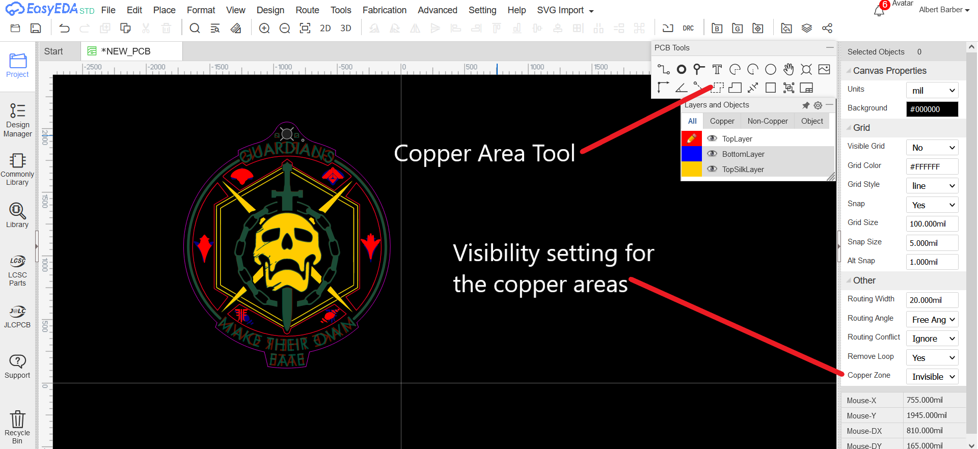

At this point, there's only one final, critical feature left to add to the PCB: the copper.
In EasyEDA, copper will only be added for features on the Top and Bottom layers. If you don't have any features on those layers, then no copper will be added to the board. In my Destiny 2 PCB example I've already placed a number of features on the solder mask layers, intending for them to be exposed copper, but without any copper underneath they will just show the raw fiberglass board material. I could go back and create a set of solid regions for each of the images, but there is an easier way: copper areas.
Copper areas are a quick way to fill an area of the board with copper. They are defined on either the Top or Bottom layers and will automatically flow around other features on the Top/Bottom and no-solid regions. This lets us easily add copper under all of our other features.
You can define a copper area using the "copper area" tool in the PCB tools menu.
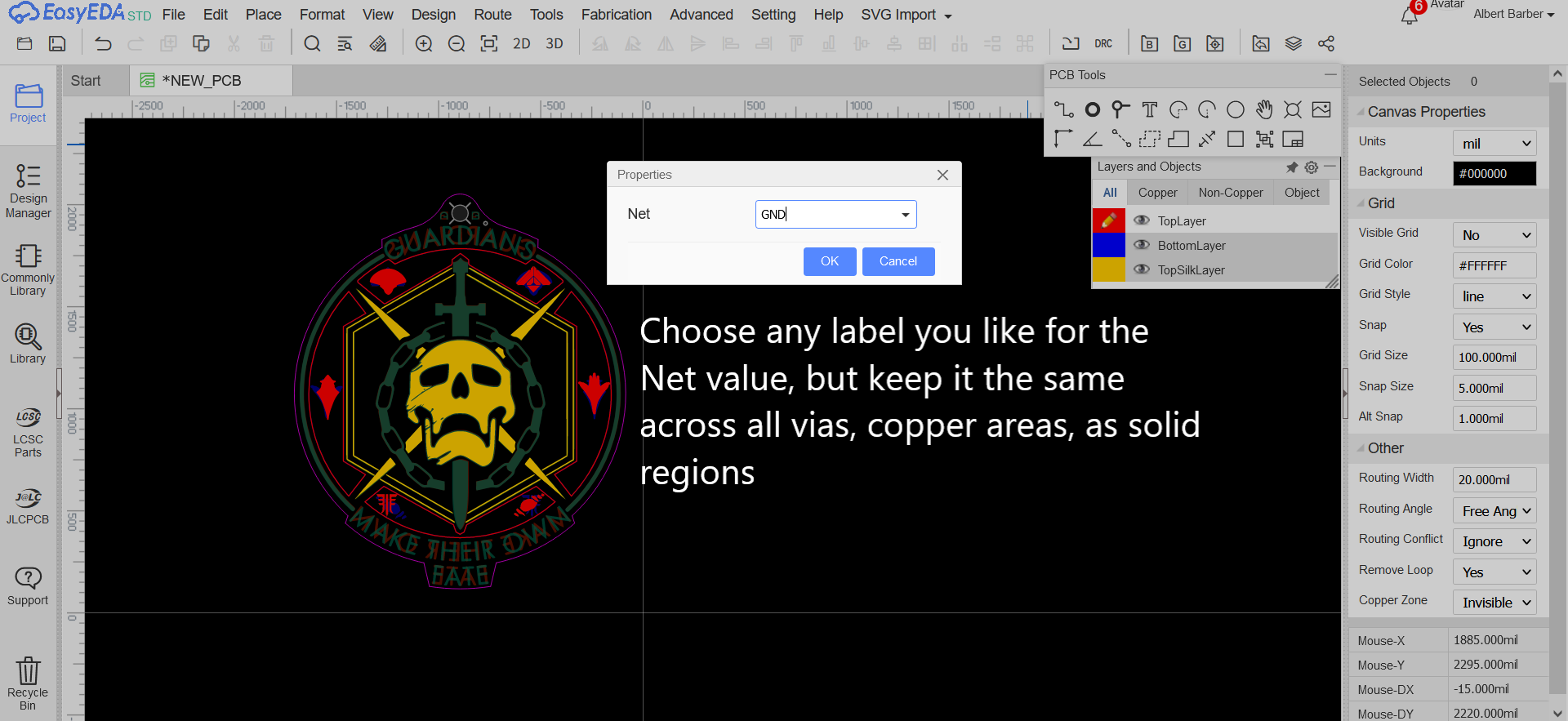
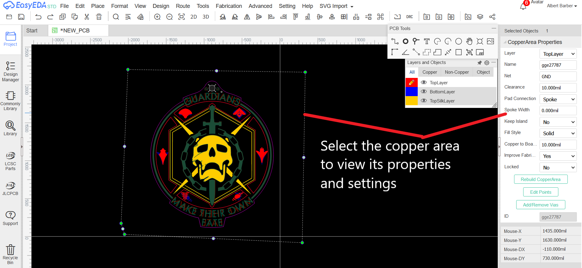
When you click on the tool it will ask you for a Net. Enter "GND". Then draw a polygon around your PCB by clicking to add points. Make sure it covers the whole PCB. Right click to finish. EasyEDA will then calculate and fill in the copper area.
EasyEDA is clever and won't fill a copper area if there's nothing for it to connect to. You can fix this in three ways:
- Set the copper area's "keep island" setting to "yes". This tells EasyEDA to fill in the copper everywhere, even if there's not an electrical connection. You can click the copper area's outline to set the "keep island" setting in the right-hand menu. This is easiest method, but doesn't let you keep areas free of copper without using no-solid regions.
- Add an electrical connection between two features on the board (on the same side). You can do this by setting their Net values to "GND". All features with the same net value are all meant to be connected together electrically. EasyEDA will connect them using the copper area.
- Add a via to the board (see Step 7) and set its Net value to "GND". The via creates a connection between both sides of the PCB, prompting EasyEDA to fill in the copper area. The extra bonus to this is that you only need one via for both the Top and Bottom layers. This is my preferred method because vias are small enough that you can place them almost anywhere, and they won't be noticeable on the final PCB.
Once to copper area is created, it may obscure other features on the PCB. You can toggle copper layers visibility as part of the canvas properties.
For images on the top/bottom copper layers, the copper fill will try to avoid them by drawing a box around the image. This can cause issues when you have multiple solid and no-solid regions with images in them. One way to avoid this is to import the image as a track and then convert it to a solid region as described in the previous steps. Another way is to set the image to be on one of the silk screen layers, re-build the copper area, and then set the image back to the copper layer. This is easier, but needs to be done every time you re-build the copper area.
For the Destiny 2 PCB I add a copper layer to both sides of the board. Note how the copper areas flow around the no-solid regions, showing that no copper will be poured there.
Exporting Gerbers
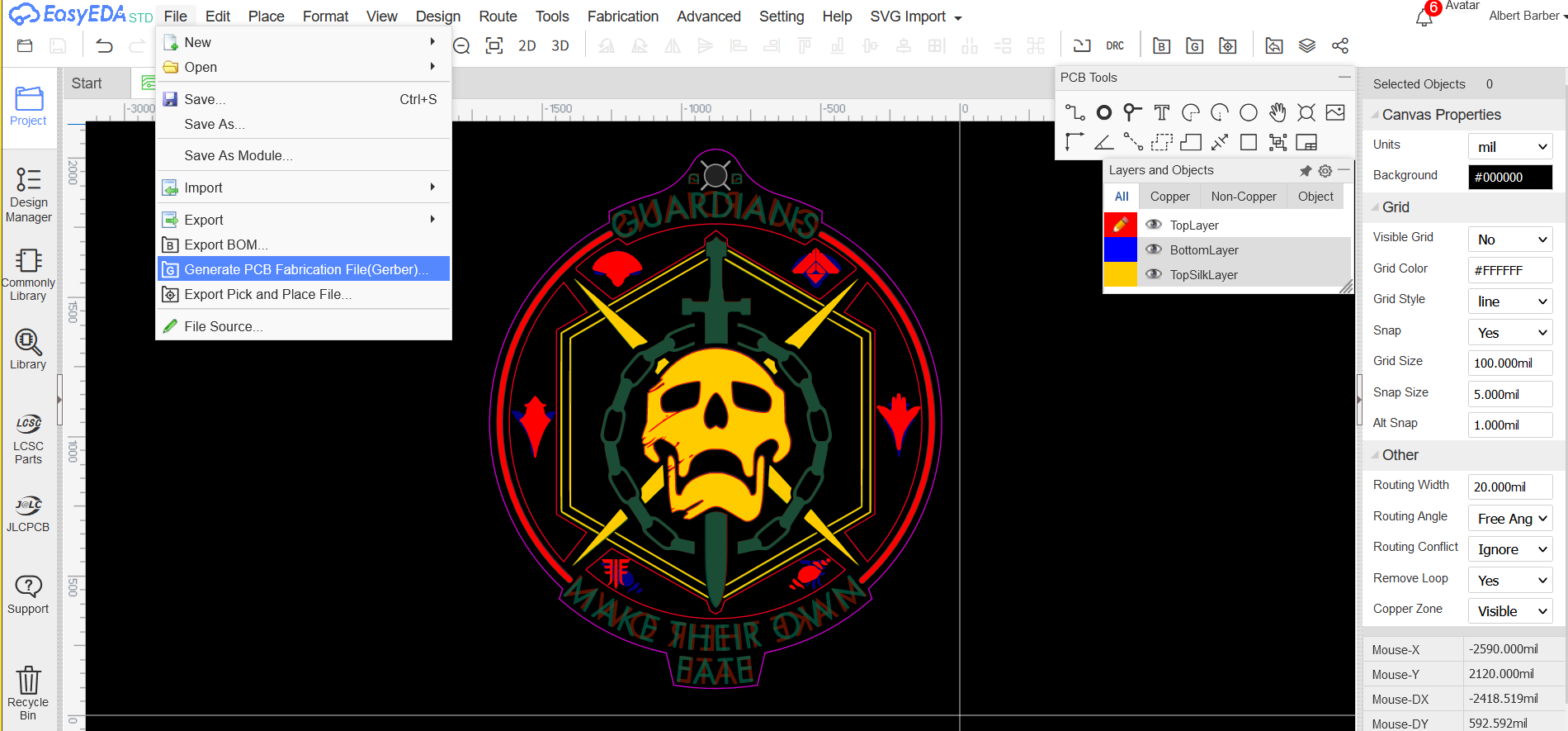
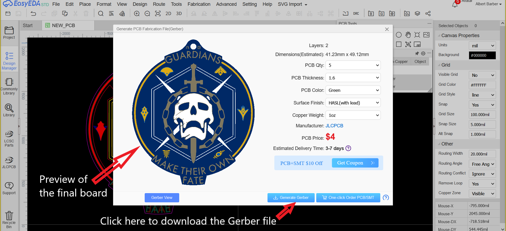
At this point your PCB is finished. It's time to export it and send it off to be made! PCB files are saved as Zipped folders, which contain a separate Gerber build file for each of the layers.
To export you PCB in EasyEDA go to "File" then "Generate PCB Fabrication File". It will ask you if you want to "DRC" (Design Rule Check). This will check that the PCB is suitable to be manufactured (I'll go over what this means in the next step). It may also ask if you want to check connections, but you can ignore this because you have none!
After the DRC you can download your Gerber file. You'll also be presented with preview of the file and the ability to order it directly from JLCPCB (ignore this for now). You should note down the dimensions of your board, or add them to the file name. This can be helpful when ordering.
To check your design you can upload it to various free Gerber viewers online. This one always works well for me. Most manufactures will give you a preview before you place an order as well.
Ordering Boards
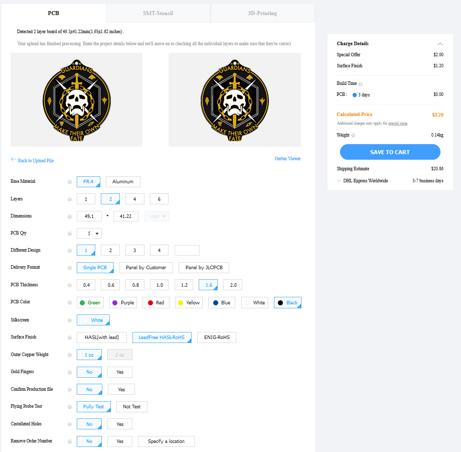
There a tons of PCB manufactures out there. Most offer a streamlined ordering process, where you simply upload your Gerber file, pick from a few options, and then order your boards. PCBShopper.com is a useful site -- it compares prices at a bunch of different board houses at once.
Usually I order from JLCPCB.com as I've had a good experience with them so far, and they offer low prices and good quality. I will note that, based on the boards I've received, their silk-screen is not as crisp as domestic (USA) manufactures. This seems to be a true of other Chinese board houses as well.
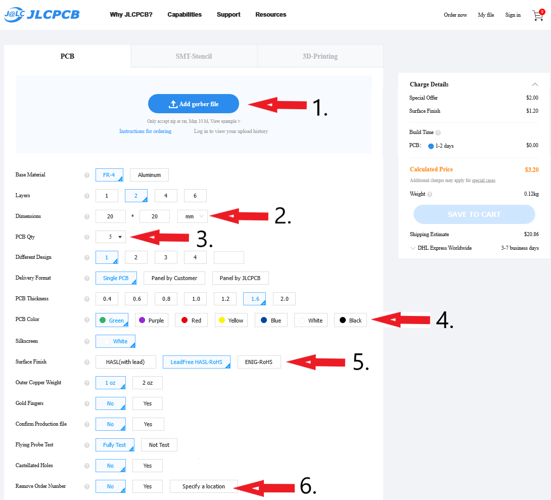
I've attached a screen shot of the JLCPCB ordering page. Most other board houses will offer a similar set of options. It may seem like there are a lot of choices, but there are only a few we actually need. I've marked these with red arrows in the image:
In order:
- At the top of the page you can upload your Gerber file. This will do some processing and then give you a preview.
- The system should also pull the dimensions from your file, but sometimes it fails for complex shapes. Here you can input the dimensions manually.
- The number of PCBs you want. You cannot order fewer than 5 PCBs at once.
- The PCB color. Note that unpopular colors may cost a bit more, or take longer to build. The most popular colors seem to be: green, blue, black, and purple.
- The surface finish. This sets how your exposed copper areas will be treated. Avoid HASL (with Lead). HASL (Lead Free) will coat the areas in solder, giving them a shiny silver look, while ENIG-RoHS will coat them in a thin layer of gold. ENIG-RoHS is much more expensive.
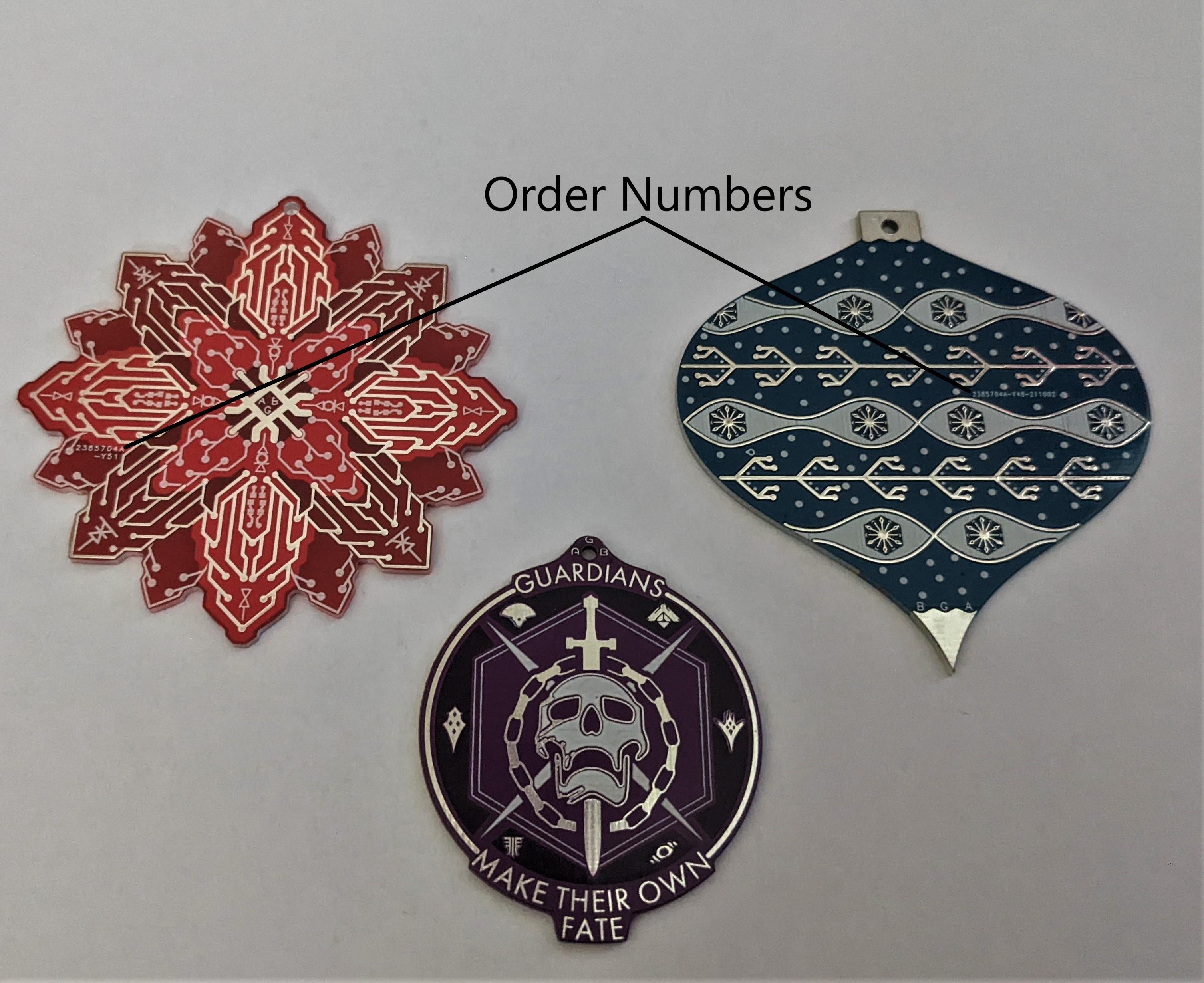
- Most PCB manufactures will add a silkscreen order number to your PCB. It will placed randomly unless you specify the location, but each manufacturer uses a different call-out, so I tend to not bother. You can opt to have the order number removed for a small additional fee. I've included a picture of the order number on a couple of my PCBs.
At this point you can finally order your PCB!
Manufacturer Constraints and Design Rules:
I will add a final note about manufacturer constraints. Each board house has its own set of capabilities, such as minimum track size, spacing requirements, etc. These are always listed somewhere on the manufacturer's website. Today, the specs are fairly consistent across the industry. When you DRC in EasyEDA it checks your board against these specs. You can modify your DRC rules to exactly match a specific manufacturer, but the defaults will work for any good board house.
The only thing that isn't covered by DRC is board cutouts. If you make part of the PCB too thin, it may break during production, so be sure to check the manufactures specs for this. I did this with my first Destiny 2 PCB design. JLCPCB warned me I was out of spec, but I had them made anyway, and luckily they turned out fine.
Whew, that was a lot. If you've made it this far, thanks for reading! I hope this was helpful, and gave you enough knowledge to give designing your own PCB a go. Keep in mind that this is just how I like to do things, there are certainly other ways and programs for doing all the steps.
If you do use this guide to make a PCB, please upload a make here, or send me a message. I'd love to see it!
If you have any questions, please leave a comment and I'll try to help.
Thanks for reading! :)