3 Channer 12V DC Relay Board
by Vaibhav K Sugandhi in Circuits > Electronics
4772 Views, 8 Favorites, 0 Comments
3 Channer 12V DC Relay Board
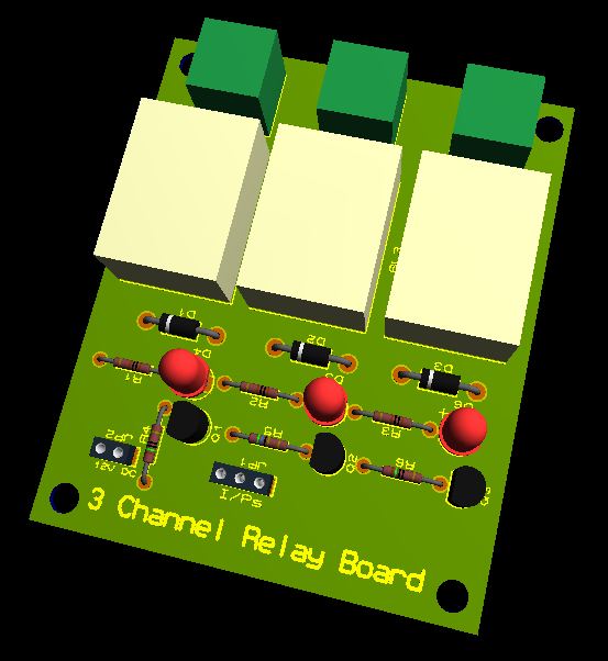
Hi everyone, I'm Mr. Vaibhav
Now a Days Relay channel is most important and required default component in the any wireless control. So in this article I'm going to show that how to make 3 channel Relay board for 12V DC, Operated by 5V DC with 200mA current.
This is for those who need Design and schematics, Who has basic knowledge about Electronics.
I listed steps for this process, Please feel free to vote, Share and comment on this.
Setup and Installation.

Today I'm going share about how to make 3 Channel DC12V Relay Board. This needs all about circuit knowledge and connections. I shared circuit diagram and PCB designs even you can copy them.
==> First we need to have Proteus V7 Software with installed libraries.
==> Then Open the suit and start your design.
Empty File and Beginning.
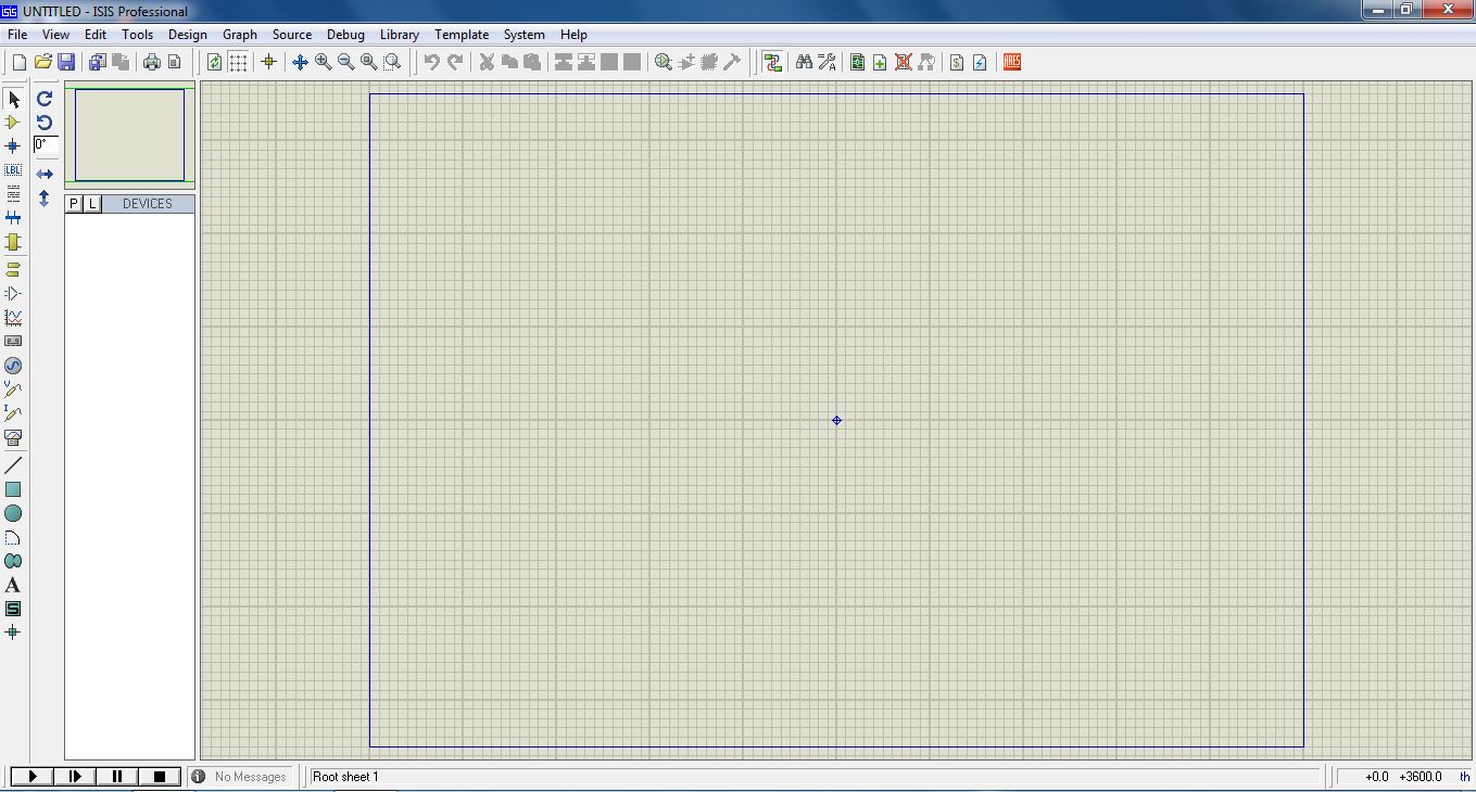
You all need to do is, Start empty project and save it first, which is good designer habit.
Then Follow the next steps.
Pic a Parts From Library.
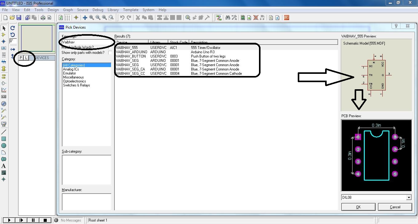
Here it is how to collect components and Parts from library, Please follow the Image for selecting the components.
Once you have all the components in list with you, then you can start you design as you wish.
Design Schematics and Circuit Connection.
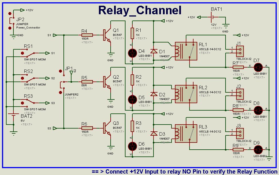
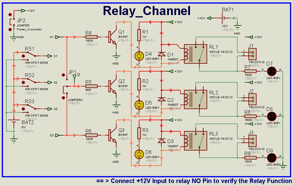
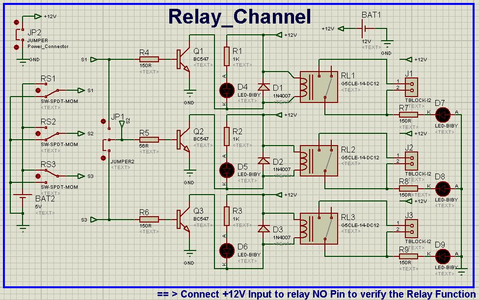
Designing the circuits and Schematics is the complicated procedure in this but this is only way to make it happen.
We all know that Schematic is the only file which Enable us to start our PCB Design. So we need to learn how to do this circuit and designs as well.
The Schematic is clearly given in all 3 Images, refer any one which you feel best.
One of the Image shows How this circuit is going to work on real time, Which you can also do it in Proteus V7. But need to go through few procedures about it.
Finally, Once your Done with circuit, then It is possible to proceed with PCB design. Hit on ARES Icon to switch the Schematic to PCB layout Editor.
ARES Editor.
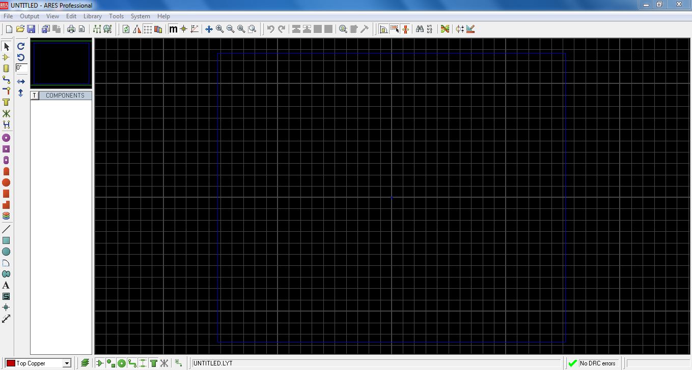
This is the place where you can place your components and make your desired PCB design.
Automatically all the components package and connection will be loaded to this editor if you done with Schematics.
So need to place component and make a tracks here.
PCB Design and Track Design.
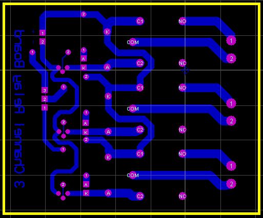
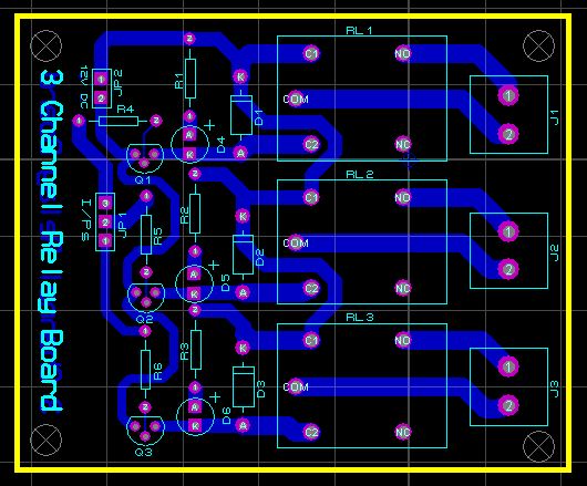
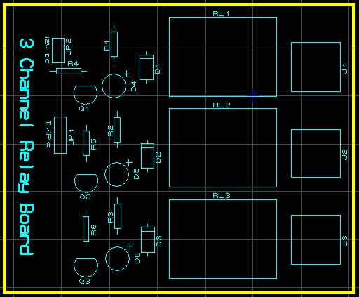
Look at the diagrams and try to make the PCB as shown, Its quite difficult for the first time. This may take a most of you time , but worth of doing this.
Please follow the IPC standards for PCB designs if your going with mass production, else just for prototyping and etching it is OK.
I uploaded bottom, Top and Silk layer designs, Please look at them.
If you done with this, Then Check with Pre Production Check Visible in Output.
If everything is OK, Then you done with your PCBs, Export it how you want and do next work.
Final Look.
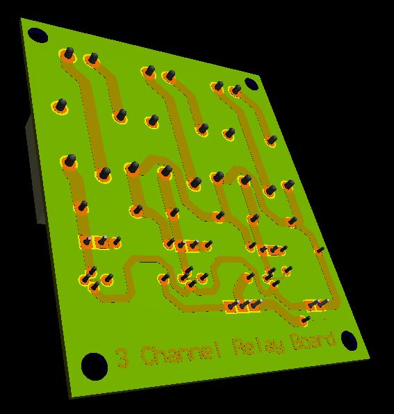
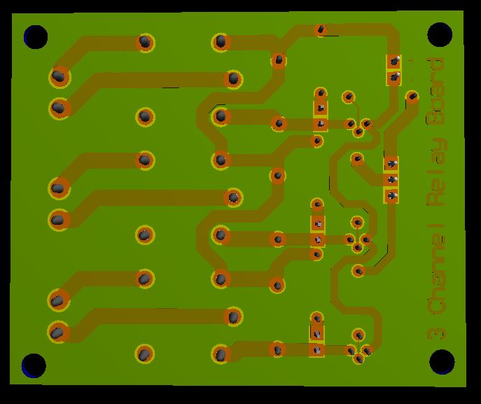

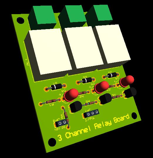
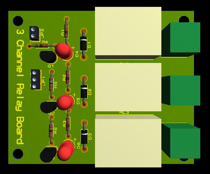
This is how it looks, If you want you can see this using Output --> 3D Visualization.
This is what i did, Even smart you can do it, But need to check with size and PCB packages.
Hope this is helpful for you,
THANK YOU ..!
If you have anything to suggest and ask, Please leave a comment to me.